


 Loading...
Texas Instruments LM258ADGKR, LM258DGKR, LM2904AVQDR, LM2904AVQPWR, LM2904DGKR Schematic [ru]
...LM158, LM158A, LM258, LM258A
LM358, LM358A, LM2904, LM2904V
www.ti.com |
SLOS068S –JUNE 1976–REVISED MAY 2013 |
Dual Operational Amplifiers
Check for Samples: LM158, LM258, LM258A, LM358, LM358A, LM2904, LM2904V
FEATURES
•Wide Supply Ranges
–Single Supply: 3 V to 32 V (26 V for LM2904)
–Dual Supplies: ±1.5 V to ±16 V (±13 V for LM2904)
•Low Supply-Current Drain, Independent of Supply Voltage: 0.7 mA Typ
•Wide Unity Gain Bandwidth: 0.7MHz
•Common-Mode Input Voltage Range Includes Ground, Allowing Direct Sensing Near Ground
•Low Input Bias and Offset Parameters
–Input Offset Voltage: 3 mV Typ A Versions: 2 mV Typ
–Input Offset Current: 2 nA Typ
–Input Bias Current: 20 nA Typ A Versions: 15 nA Typ
•Differential Input Voltage Range Equal to Maximum-Rated Supply Voltage: 32 V (26 V for LM2904)
•Open-Loop Differential Voltage Gain: 100dB Typ
•Internal Frequency Compensation
•On Products Compliant to MIL-PRF-38535, All Parameters Are Tested Unless Otherwise Noted. On All Other Products, Production Processing Does Not Necessarily Include Testing of All Parameters.
LM158, LM158A . . . JG Package LM258, LM258A . . . D, DGK, or P Package LM358 . . . D, DGK, P, PS, or PW Package
LM358A . . . D, DGK, P, or PW Package LM2904 . . . D, DGK, P, PS, or PW Package (Top View)
1OUT |
|
|
1 |
8 |
|
VCC |
|
|
|
||||
1IN− |
|
2 |
7 |
|
2OUT |
|
1IN+ |
|
3 |
6 |
|
2IN− |
|
GND |
|
4 |
5 |
|
2IN+ |
|
|
|
|
|
|
|
|
DESCRIPTION
These devices consist of two independent, high-gain frequency-compensated operational amplifiers designed to operate from a single supply over a wide range of voltages. Operation from split supplies also is possible if the difference between the two supplies
is 3 V to 32 V (3 V to 26 V for the LM2904), and VCC is at least 1.5 V more positive than the input
common-mode voltage. The low supply-current drain is independent of the magnitude of the supply voltage.
Applications include transducer amplifiers, dc amplification blocks, and all the conventional operational amplifier circuits that now can be implemented more easily in single-supply-voltage systems. For example, these devices can be operated directly from the standard 5-V supply used in digital systems and easily can provide the required interface electronics without additional ±5-V supplies.
LM158, LM158A . . . FK Package |
||||||
|
(Top View) |
|
||||
|
NC |
1OUT |
|
CC+ |
NC |
|
|
NC V |
|
||||
NC |
3 |
2 |
1 |
20 19 |
NC |
|
4 |
|
|
|
18 |
||
1IN− |
5 |
|
|
|
17 |
2OUT |
NC |
6 |
|
|
|
16 |
NC |
1IN+ |
7 |
|
|
|
15 |
2IN− |
NC |
8 |
|
|
|
14 |
NC |
|
9 |
10 11 12 13 |
|
|||
|
NC |
GND |
NC |
2IN+ |
NC |
|
NC − No internal connection
Please be aware that an important notice concerning availability, standard warranty, and use in critical applications of Texas Instruments semiconductor products and disclaimers thereto appears at the end of this data sheet.
PRODUCTION DATA information is current as of publication date. |
Copyright © 1976–2013, Texas Instruments Incorporated |
Products conform to specifications per the terms of the Texas |
|
Instruments standard warranty. Production processing does not |
|
necessarily include testing of all parameters. |
|
LM158, LM158A, LM258, LM258A
LM358, LM358A, LM2904, LM2904V
SLOS068S –JUNE 1976–REVISED MAY 2013 |
www.ti.com |
This integrated circuit can be damaged by ESD. Texas Instruments recommends that all integrated circuits be handled with appropriate precautions. Failure to observe proper handling and installation procedures can cause damage.
ESD damage can range from subtle performance degradation to complete device failure. Precision integrated circuits may be more susceptible to damage because very small parametric changes could cause the device not to meet its published specifications.
Symbol (Each Amplifier)
IN+ |
|
|
|
|
+ |
|
OUT |
||
|
|
|||
IN− |
|
− |
|
|
|
|
|
||
|
|
|
||
|
|
|
|
|
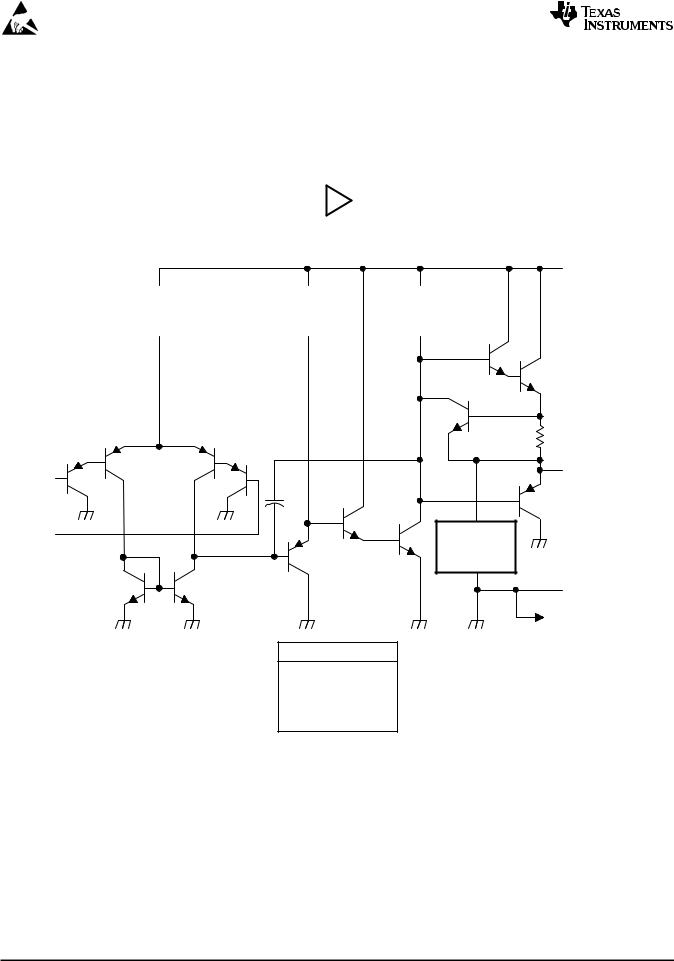
Schematic (Each Amplifier)
VCC+
≈6-µA |
|
≈6-µA |
|
≈100-µA |
|
|
Current |
|
Current |
|
Current |
|
|
Regulator |
|
Regulator |
|
Regulator |
|
|
|
|
|
|
|
|
|
|
|
|
|
|
|
|
|
|
|
|
|
|
|
OUT
IN−
IN+ |
≈50-µA |
Current
Regulator
GND (or VCC−)
To Other Amplifier
COMPONENT COUNT
EPI-FET 1
DIODES 2
RESISTORS 7
TRANSISTORS 51
CAPACITORS 2
2 |
Submit Documentation Feedback |
Copyright © 1976–2013, Texas Instruments Incorporated |
Product Folder Links: LM158 LM258 LM258A LM358 LM358A LM2904 LM2904V

|
|
|
|
|
LM158, |
LM158A, LM258, LM258A |
|||
www.ti.com |
|
|
|
|
LM358, LM358A, LM2904, LM2904V |
||||
|
|
|
|
SLOS068S –JUNE 1976–REVISED MAY 2013 |
|||||
Absolute Maximum Ratings |
|
|
|
|
|
|
|
|
|
over operating free-air temperature range (unless otherwise noted)(1) |
|
|
|
|
|
|
|||
|
|
|
|
|
|
|
LM158, |
|
|
|
|
|
|
|
|
|
LM158A |
|
|
|
|
|
|
|
|
|
LM258, |
|
|
|
|
|
|
|
|
|
LM258A |
LM2904 |
UNIT |
|
|
|
|
|
|
|
LM358, |
|
|
|
|
|
|
|
|
|
LM358A |
|
|
|
|
|
|
|
|
|
LM2904V |
|
|
(2) |
|
|
|
|
|
|
±16 or 32 |
±13 or 26 |
V |
Supply voltage, VCC |
|
|
|
|
|
|
|||
Differential input voltage, VID(3) |
|
|
|
|
|
|
±32 |
±26 |
V |
Input voltage, VI (either input) |
|
|
|
|
|
|
–0.3 to 32 |
–0.3 to 26 |
V |
Duration of output short circuit (one amplifier) to ground at (or below) T |
A |
= 25°C, V |
CC |
≤ 15 V(4) |
|
Unlimited |
Unlimited |
|
|
|
|
|
|
|
|
|
|
||
|
D package |
|
|
|
97 |
97 |
|
||
|
DGK package |
|
|
|
172 |
172 |
|
||
Package thermal impedance, θJA(4)(5) |
P package |
|
|
|
85 |
85 |
°C/W |
||
|
PS package |
|
|
|
95 |
95 |
|
||
|
PW package |
|
|
|
149 |
149 |
|
||
|
D package |
|
|
|
72.2 |
|
|
||
Package thermal impedance, θJC (6)(7) |
FK package |
|
|
|
5.61 |
|
°C/W |
||
|
JG package |
|
|
|
14.5 |
|
|
||
|
LM158, LM158A |
|
|
|
–55 to 125 |
|
|
||
Operating free air temperature range. TA |
LM258, LM258A |
|
|
|
–25 to 85 |
|
°C |
||
LM358, LM358A |
|
|
|
0 to 70 |
|
||||
|
|
|
|
|
|
||||
|
LM2904 |
|
|
|
|
–40 to 125 |
–40 to 125 |
|
|
Operating virtual junction temperature, TJ |
|
|
|
|
|
|
150 |
150 |
°C |
Case temperature for 60 seconds |
FK package |
|
|
|
260 |
|
°C |
||
Lead temperature 1,6 mm (1/16 inch) from case for 60 |
JG package |
|
|
|
300 |
300 |
°C |
||
seconds |
|
|
|
||||||
|
|
|
|
|
|
|
|
|
|
Storage temperature range, Tstg |
|
|
|
|
|
|
–65 to 150 |
–65 to 150 |
°C |
(1)Stresses beyond those listed under Absolute Maximum Ratings may cause permanent damage to the device. These are stress ratings only, and functional operation of the device at these or any other conditions beyond those indicated under Recommended Operating Conditions is not implied. Exposure to absolute-maximum-rated conditions for extended periods may affect device reliability.
(2)All voltage values (except differential voltages and VCC specified for the measurement of IOS) are with respect to the network GND.
(3)Differential voltages are at IN+, with respect to IN−.
(4)Short circuits from outputs to VCC can cause excessive heating and eventual destruction.
(5)Maximum power dissipation is a function of TJ(max), θJA, and TA. The maximum allowable power dissipation at any allowable ambient temperature is PD = (TJ(max) – TA)/θJA. Operating at the absolute maximum TJ of 150°C can affect reliability.
(6)Maximum power dissipation is a function of TJ(max), θJC, and TC. The maximum allowable power dissipation at any allowable case temperature is PD = (TJ(max) – TC)/θJC. Operating at the absolute maximum TJ of 150°C can affect reliability.
(7)The package thermal impedance is calculated in accordance with MIL-STD-883.
Copyright © 1976–2013, Texas Instruments Incorporated |
Submit Documentation Feedback |
3 |
Product Folder Links: LM158 LM258 LM258A LM358 LM358A LM2904 LM2904V

LM158, |
LM158A, LM258, LM258A |
|
|
|
|
|
|
|
|
|
|
||
LM358, LM358A, LM2904, LM2904V |
|
|
|
|
|
|
|
|
www.ti.com |
||||
SLOS068S –JUNE 1976–REVISED MAY 2013 |
|
|
|
|
|
|
|
|
|||||
Electrical Characteristics |
|
|
|
|
|
|
|
|
|
|
|
|
|
at specified free-air temperature, VCC = 5 V (unless otherwise noted) |
|
|
|
|
|
|
|
||||||
|
PARAMETER |
TEST CONDITIONS(1) |
TA(2) |
|
LM158 LM258 |
|
|
LM358 |
|
UNIT |
|||
|
|
MIN |
TYP(3) |
MAX |
MIN |
TYP(3) |
MAX |
||||||
|
|
|
|
|
|
|
|
||||||
VIO |
Input offset voltage |
VCC = 5 V to MAX, VIC = VICRmin, |
25°C |
|
|
3 |
5 |
|
3 |
7 |
mV |
||
VO = 1.4 V |
|
Full range |
|
|
|
7 |
|
|
9 |
||||
|
|
|
|
|
|
|
|
|
|||||
αVIO |
Average temperature coefficient of |
|
|
|
Full range |
|
|
7 |
|
|
7 |
|
µV/°C |
input offset voltage |
|
|
|
|
|
|
|
|
|||||
|
|
|
|
|
|
|
|
|
|
|
|
|
|
IIO |
Input offset current |
VO = 1.4 V |
|
25°C |
|
|
2 |
30 |
|
2 |
50 |
nA |
|
|
Full range |
|
|
|
100 |
|
|
150 |
|||||
|
|
|
|
|
|
|
|
|
|
|
|||
αIIO |
Average temperature coefficient of |
|
|
|
Full range |
|
|
10 |
|
|
10 |
|
pA/°C |
input offset current |
|
|
|
|
|
|
|
|
|||||
|
|
|
|
|
|
|
|
|
|
|
|
|
|
IIB |
Input bias current |
VO = 1.4 V |
|
25°C |
|
|
–20 |
–150 |
|
–20 |
–250 |
nA |
|
|
|
|
|
|
|
|
|
|
|||||
|
Full range |
|
|
|
–300 |
|
|
–500 |
|||||
|
|
|
|
|
|
|
|
|
|
|
|||
|
|
|
|
|
|
|
|
|
|
|
|
|
|
|
|
|
|
|
25°C |
|
0 to |
|
|
0 to |
|
|
|
|
|
|
|
|
|
VCC – 1.5 |
|
|
VCC – 1.5 |
|
|
|
|
VICR |
Common-mode input voltage range |
VCC = 5 V to MAX |
|
|
|
|
|
|
|
V |
|||
|
Full range |
|
0 to |
|
|
0 to |
|
|
|||||
|
|
|
|
|
|
|
|
|
|
|
|||
|
|
|
|
|
|
VCC – 2 |
|
|
VCC – 2 |
|
|
|
|
|
|
|
|
|
|
|
|
|
|
|
|
||
|
|
RL ≥ 2 kΩ |
|
25°C |
|
VCC – 1.5 |
|
|
VCC – 1.5 |
|
|
|
|
VOH |
High-level output voltage |
RL ≥ 10 kΩ |
|
25°C |
|
|
|
|
|
|
|
V |
|
VCC = MAX |
|
RL = 2 kΩ |
Full range |
|
26 |
|
|
26 |
|
|
|||
|
|
|
|
|
|
|
|
|
|||||
|
|
|
RL ≥ 10 kΩ |
Full range |
|
27 |
28 |
|
27 |
28 |
|
|
|
|
|
|
|
|
|
|
|
||||||
VOL |
Low-level output voltage |
RL ≤ 10 kΩ |
|
Full range |
|
|
5 |
20 |
|
5 |
20 |
mV |
|
|
Large-signal differential voltage |
VCC = 15 V |
|
25°C |
|
50 |
100 |
|
25 |
100 |
|
|
|
AVD |
VO = 1 V to 11 V, |
|
|
|
|
|
|
|
|
|
V/mV |
||
amplification |
|
Full range |
|
25 |
|
|
15 |
|
|
||||
|
RL ≥ 2 kΩ |
|
|
|
|
|
|
|
|||||
|
|
|
|
|
|
|
|
|
|||||
|
|
|
|
|
|
|
|
|
|
|
|
||
CMRR |
Common-mode rejection ratio |
VCC= 5 V to MAX, |
|
25°C |
|
70 |
80 |
|
65 |
80 |
|
dB |
|
VIC = VICR(min) |
|
|
|
|
|||||||||
|
|
|
|
|
|
|
|
|
|
|
|
||
kSVR |
Supply-voltage rejection ratio |
VCC = 5 V to MAX |
|
25°C |
|
65 |
100 |
|
65 |
100 |
|
dB |
|
( VDD / VIO) |
|
|
|
|
|||||||||
|
|
|
|
|
|
|
|
|
|
|
|
|
|
VO1/ VO2 |
Crosstalk attenuation |
f = 1 kHz to 20 kHz |
|
25°C |
|
|
120 |
|
|
120 |
|
dB |
|
|
|
VCC = 15 V, |
|
|
25°C |
|
–20 |
–30 |
|
–20 |
–30 |
|
|
|
|
VID = 1 V, |
|
Source |
Full range |
|
–10 |
|
|
–10 |
|
|
|
|
|
VO = 0 |
|
|
|
|
|
|
|
|
|||
|
|
|
|
|
|
|
|
|
|
|
|
mA |
|
IO |
Output current |
VCC = 15 V, |
|
|
25°C |
|
10 |
20 |
|
10 |
20 |
|
|
|
|
|
|
|
|
||||||||
|
|
VID = –1 V, |
|
Sink |
Full range |
|
5 |
|
|
5 |
|
|
|
|
|
VO = 15 V |
|
|
|
|
|
|
|
|
|||
|
|
|
|
|
|
|
|
|
|
|
|
|
|
|
|
VID = –1 V, VO = 200 mV |
25°C |
|
12 |
30 |
|
12 |
30 |
|
μA |
||
IOS |
Short-circuit output current |
VCC at 5 V, VO = 0, |
|
25°C |
|
|
±40 |
±60 |
|
±40 |
±60 |
mA |
|
GND at –5 V |
|
|
|
|
|||||||||
|
|
|
|
|
|
|
|
|
|
|
|
||
|
|
|
|
|
|
|
|
|
|
|
|
|
|
|
|
VO = 2.5 V, No load |
|
Full range |
|
|
0.7 |
1.2 |
|
0.7 |
1.2 |
|
|
ICC |
Supply current (two amplifiers) |
VCC = MAX, VO = 0.5 VCC, |
Full range |
|
|
1 |
2 |
|
1 |
2 |
mA |
||
|
|
No load |
|
|
|
|
|
||||||
|
|
|
|
|
|
|
|
|
|
|
|
||
(1)All characteristics are measured under open-loop conditions, with zero common-mode input voltage, unless otherwise specified. MAX VCC for testing purposes is 26 V for LM2902 and 30 V for the others.
(2)Full range is –55°C to 125°C for LM158, –25°C to 85°C for LM258, and 0°C to 70°C for LM358, and –40°C to 125°C for LM2904 .
(3)All typical values are at TA = 25°C
4 |
Submit Documentation Feedback |
Copyright © 1976–2013, Texas Instruments Incorporated |
Product Folder Links: LM158 LM258 LM258A LM358 LM358A LM2904 LM2904V

|
|
|
|
LM158, |
LM158A, LM258, LM258A |
||||
www.ti.com |
|
|
|
LM358, LM358A, LM2904, LM2904V |
|||||
|
|
|
|
SLOS068S –JUNE 1976–REVISED MAY 2013 |
|||||
Electrical Characteristics |
|
|
|
|
|
|
|
|
|
at specified free-air temperature, VCC = 5 V (unless otherwise noted) |
|
|
|
|
|
|
|||
|
PARAMETER |
TEST CONDITIONS(1) |
TA(2) |
|
|
LM2904 |
|
UNIT |
|
|
|
MIN |
TYP(3) |
MAX |
|||||
|
|
|
|
|
|
|
|||
|
|
VCC = 5 V to MAX, |
Non-A-suffix |
25°C |
|
|
3 |
7 |
|
|
|
devices |
Full range |
|
|
|
10 |
|
|
VIO |
Input offset voltage |
VIC = VICR(min), |
|
|
|
|
mV |
||
|
|
|
|
|
|
||||
|
25°C |
|
|
1 |
2 |
||||
|
|
VO = 1.4 V |
A-suffix devices |
|
|
|
|||
|
|
|
|
|
|
|
|
||
|
|
Full range |
|
|
|
4 |
|
||
|
|
|
|
|
|
|
|||
|
|
|
|
|
|
|
|
||
|
|
|
|
|
|
|
|
|
|
αVIO |
Average temperature coefficient of input |
|
|
Full range |
|
|
7 |
|
μV/°C |
offset voltage |
|
|
|
|
|
||||
|
|
|
|
|
|
|
|
|
|
|
|
|
Non-V device |
25°C |
|
|
2 |
50 |
|
|
|
|
|
|
|
|
|
|
|
IIO |
Input offset current |
VO = 1.4 V |
Full range |
|
|
|
300 |
nA |
|
|
|
|
|
||||||
|
|
|
|
|
|
||||
V-suffix device |
25°C |
|
|
2 |
50 |
||||
|
|
|
|
|
|
||||
|
|
|
|
|
|
|
|
|
|
|
|
|
Full range |
|
|
|
150 |
|
|
|
|
|
|
|
|
|
|
||
|
|
|
|
|
|
|
|
|
|
αIIO |
Average temperature coefficient of input |
|
|
Full range |
|
|
10 |
|
pA/°C |
offset current |
|
|
|
|
|
||||
|
|
|
|
|
|
|
|
|
|
IIB |
Input bias current |
VO = 1.4 V |
|
25°C |
|
|
–20 |
–250 |
nA |
|
|
|
|
|
|
||||
|
Full range |
|
|
|
–500 |
||||
|
|
|
|
|
|
|
|
||
|
|
|
|
|
|
|
|
|
|
|
|
|
|
25°C |
|
0 to |
|
|
|
|
|
|
|
VCC – 1.5 |
|
|
|
||
VICR |
Common-mode input voltage range |
VCC = 5 V to MAX |
|
|
|
|
V |
||
|
Full range |
|
0 to |
|
|
||||
|
|
|
|
|
|
|
|
||
|
|
|
|
|
VCC – 2 |
|
|
|
|
|
|
|
|
|
|
|
|
|
|
|
|
RL ≥ 10 kΩ |
|
25°C |
VCC − 1.5 |
|
|
|
|
|
|
VCC = MAX, |
RL = 2 kΩ |
Full range |
|
22 |
|
|
|
VOH |
High-level output voltage |
Non-V device |
RL ≥ 10 kΩ |
Full range |
|
23 |
24 |
|
V |
|
|
|
|||||||
|
|
VCC = MAX |
RL = 2 kΩ |
Full range |
|
26 |
|
|
|
|
|
V-suffix device |
RL ≥ 10 kΩ |
Full range |
|
27 |
28 |
|
|
|
|
|
|
|
|
||||
VOL |
Low-level output voltage |
RL ≤ 10 kΩ |
|
Full range |
|
|
5 |
20 |
mV |
|
|
VCC = 15 V, |
|
25°C |
|
25 |
100 |
|
|
AVD |
Large-signal differential voltage amplification |
VO = 1 V to 11 V, |
|
Full range |
|
15 |
|
|
V/mV |
|
|
RL ≥ 2 kΩ |
|
|
|
|
|
||
|
|
|
|
|
|
|
|
|
|
CMRR |
Common-mode rejection ratio |
VCC = 5V to MAX, |
Non-V device |
25°C |
|
50 |
80 |
|
dB |
|
|
|
|
|
|
||||
VIC = VICR(min) |
V-suffix device |
25°C |
|
65 |
80 |
|
|||
|
|
|
|
|
|||||
kSVR |
Supply-voltage rejection ratio |
VCC = 5 V to MAX |
|
25°C |
|
65 |
100 |
|
dB |
( VCC / VIO) |
|
|
|
||||||
|
|
|
|
|
|
|
|
|
|
VO1/ VO2 |
Crosstalk attenuation |
f = 1 kHz to 20 kHz |
|
25°C |
|
|
120 |
|
dB |
|
|
VCC = 15 V, |
|
25°C |
|
–20 |
–30 |
|
|
|
|
VID = 1 V, |
Source |
Full range |
|
–10 |
|
|
|
|
|
VO = 0 |
|
|
|
|
|
||
|
|
|
|
|
|
|
|
mA |
|
IO |
Output current |
VCC = 15 V, |
|
25°C |
|
10 |
20 |
|
|
|
|
|
|
||||||
VID = –1 V, |
Sink |
Full range |
|
5 |
|
|
|
||
|
|
|
|
|
|
||||
|
|
VO = 15 V |
|
|
|
|
|
||
|
|
|
|
|
|
|
|
|
|
|
|
VID = –1 V, VO = 200 mV |
Non-V device |
25°C |
|
|
30 |
|
μA |
|
|
|
|
|
|
|
|
||
|
|
V-suffix device |
25°C |
|
12 |
40 |
|
||
|
|
|
|
|
|
||||
|
|
|
|
|
|
|
|
|
|
IOS |
Short-circuit output current |
VCC at 5 V, VO = 0, GND at −5 V |
25°C |
|
|
±40 |
±60 |
mA |
|
ICC |
Supply current (four amplifiers) |
VO = 2.5 V, No load |
|
Full range |
|
|
0.7 |
1.2 |
mA |
VCC = MAX, VO = 0.5 VCC, No load |
Full range |
|
|
1 |
2 |
||||
(1)All characteristics are measured under open-loop conditions, with zero common-mode input voltage, unless otherwise specified. MAX VCC for testing purposes is 26 V for LM2902 and 32 V for LM2902V.
(2)Full range is –55°C to 125°C for LM158, –25°C to 85°C for LM258, 0°C to 70°C for LM358, and –40°C to 125°C for LM2904.
(3)All typical values are at TA = 25°C.
Copyright © 1976–2013, Texas Instruments Incorporated |
Submit Documentation Feedback |
5 |
Product Folder Links: LM158 LM258 LM258A LM358 LM358A LM2904 LM2904V

LM158, |
LM158A, LM258, LM258A |
|
|
|
|
|
|
|
|
||||
LM358, LM358A, LM2904, LM2904V |
|
|
|
|
|
|
www.ti.com |
||||||
SLOS068S –JUNE 1976–REVISED MAY 2013 |
|
|
|
|
|
|
|
||||||
Electrical Characteristics |
|
|
|
|
|
|
|
|
|
||||
at specified free-air temperature, VCC = 5 V (unless otherwise noted) |
|
|
|
|
|
|
|||||||
PARAMETER |
TEST CONDITIONS(1) |
TA(1) |
|
LM158A |
|
|
LM258A |
|
UNIT |
||||
MIN |
TYP(2) |
MAX |
MIN |
TYP(2) |
MAX |
||||||||
|
|
|
|
|
|
|
|||||||
|
|
VCC = 5 V to 30 V, |
|
25°C |
|
|
2 |
|
2 |
3 |
|
||
VIO |
Input offset voltage |
VIC = VICR(min), |
|
Full range |
|
|
4 |
|
|
4 |
mV |
||
|
|
VO = 1.4 V |
|
|
|
|
|
|
|||||
|
|
|
|
|
|
|
|
|
|
|
|||
|
Average |
|
|
|
|
|
|
|
|
|
|
|
|
αVIO |
temperature |
|
|
|
Full range |
|
7 |
15(3) |
|
7 |
15 |
µA/°C |
|
|
coefficient of input |
|
|
|
|
|
|
|
|
|
|
|
|
|
offset voltage |
|
|
|
|
|
|
|
|
|
|
|
|
IIO |
Input offset current |
VO = 1.4 V |
|
25°C |
|
2 |
10 |
|
2 |
15 |
nA |
||
|
|
|
|
|
|
|
|
||||||
|
Full range |
|
|
30 |
|
|
30 |
||||||
|
|
|
|
|
|
|
|
|
|
||||
|
|
|
|
|
|
|
|
|
|
|
|
|
|
|
Average |
|
|
|
|
|
|
|
|
|
|
|
|
αIIO |
temperature |
|
|
|
Full range |
|
10 |
200 |
|
10 |
200 |
pA/°C |
|
coefficient of input |
|
|
|
|
|
||||||||
|
|
|
|
|
|
|
|
|
|
|
|
||
|
offset current |
|
|
|
|
|
|
|
|
|
|
|
|
|
|
|
|
|
|
|
|
|
|
|
|
|
|
IIB |
Input bias current |
VO = 1.4 V |
|
25°C |
|
–15 |
–50 |
|
–15 |
–80 |
nA |
||
|
|
|
|
|
|
|
|
||||||
|
Full range |
|
|
–100 |
|
|
–100 |
||||||
|
|
|
|
|
|
|
|
|
|
||||
|
|
|
|
|
|
|
|
|
|
|
|
|
|
|
|
|
|
|
25°C |
0 to |
|
|
0 to |
|
|
|
|
|
Common-mode |
|
|
|
VCC – 1.5 |
|
|
VCC – 1.5 |
|
|
|
||
VICR |
VCC = 30 V |
|
|
|
|
|
|
V |
|||||
input voltage range |
|
Full range |
0 to |
|
|
0 to |
|
|
|||||
|
|
|
|
|
|
|
|
|
|||||
|
|
|
|
|
|
|
|
|
|
||||
|
|
|
|
|
VCC – 2 |
|
|
VCC – 2 |
|
|
|
||
|
|
|
|
|
|
|
|
|
|
|
|||
|
High-level output |
RL ≥ 2 kΩ |
|
25°C |
VCC – 1.5 |
|
|
VCC – 1.5 |
|
|
|
||
VOH |
|
|
RL= 2kΩ |
Full range |
26 |
|
|
26 |
|
|
V |
||
voltage |
VCC = 30 V |
|
|
|
|
|
|||||||
|
|
|
RL≥ 10kΩ |
Full range |
27 |
28 |
|
27 |
28 |
|
|
||
|
|
|
|
|
|
|
|||||||
VOL |
Low-level output |
RL ≤ 10 kΩ |
|
Full range |
|
5 |
20 |
|
5 |
20 |
mV |
||
voltage |
|
|
|
||||||||||
|
|
|
|
|
|
|
|
|
|
|
|
||
|
Large-signal |
VCC = 15 V, VO = 1 V to 11 V, |
25°C |
50 |
100 |
|
50 |
100 |
|
|
|||
AVD |
differential voltage |
|
|
|
|
|
|
|
V/mV |
||||
|
|
|
|
|
|
|
|||||||
RL ≥ 2 kΩ |
|
Full range |
25 |
|
|
25 |
|
|
|||||
|
amplification |
|
|
|
|
|
|
||||||
|
|
|
|
|
|
|
|
|
|
|
|
|
|
CMRR |
Common-mode |
|
|
|
25°C |
70 |
80 |
|
70 |
80 |
|
dB |
|
rejection ratio |
|
|
|
|
|
||||||||
|
|
|
|
|
|
|
|
|
|
|
|
||
|
Supply-voltage |
|
|
|
|
|
|
|
|
|
|
|
|
kSVR |
rejection ratio |
|
|
|
25°C |
65 |
100 |
|
65 |
100 |
|
dB |
|
|
( VD / VIO) |
|
|
|
|
|
|
|
|
|
|
|
|
VO1/ VO2 |
Crosstalk |
f = 1 kHz to 20 kHz |
25°C |
|
120 |
|
|
120 |
|
dB |
|||
attenuation |
|
|
|
|
|||||||||
|
|
|
|
|
|
|
|
|
|
|
|
||
|
|
VCC = 15 V, |
|
|
25°C |
–20 |
–30 |
–60 |
–20 |
–30 |
−60 |
|
|
|
|
VID = 1 V, |
|
Source |
Full range |
–10 |
|
|
–10 |
|
|
|
|
|
|
VO = 0 |
|
|
|
|
|
|
|
||||
|
|
|
|
|
|
|
|
|
|
|
mA |
||
IO |
Output current |
VCC = 15 V, |
|
|
25°C |
10 |
20 |
|
10 |
20 |
|
||
|
|
|
|
|
|||||||||
|
|
VID = –1 V, |
|
Sink |
Full range |
5 |
|
|
5 |
|
|
|
|
|
|
VO = 15 V |
|
|
|
|
|
|
|
||||
|
|
|
|
|
|
|
|
|
|
|
|
||
|
|
VID = −1 V, VO = 200 mV |
25°C |
12 |
30 |
|
12 |
30 |
|
μA |
|||
IOS |
Short-circuit output |
VCC at 5 V, GND at –5 V, |
25°C |
|
±40 |
±60 |
|
±40 |
±60 |
mA |
|||
current |
VO = 0 |
|
|
|
|||||||||
|
|
|
|
|
|
|
|
|
|
||||
|
Supply current (four |
VO = 2.5 V, No load |
Full range |
|
0.7 |
1.2 |
|
0.7 |
1.2 |
|
|||
ICC |
VCC = MAX V, VO = 0.5 V, |
|
|
|
|
|
|
|
mA |
||||
amplifiers) |
Full range |
|
1 |
2 |
|
1 |
2 |
||||||
|
|
No load |
|
|
|
|
|||||||
|
|
|
|
|
|
|
|
|
|
|
|||
(1)All characteristics are measured under open-loop conditions, with zero common-mode input voltage, unless otherwise specified. MAX VCC for testing purposes is 26 V for LM2904 and 30 V for others.
(2)All typical values are at TA = 25°C.
(3)On products compliant to MIL-PRF-38535, this parameter is not production tested.
6 |
Submit Documentation Feedback |
Copyright © 1976–2013, Texas Instruments Incorporated |
Product Folder Links: LM158 LM258 LM258A LM358 LM358A LM2904 LM2904V

LM158, LM158A, LM258, LM258A
LM358, LM358A, LM2904, LM2904V
www.ti.com |
SLOS068S –JUNE 1976–REVISED MAY 2013 |
Electrical Characteristics
at specified free-air temperature, VCC = 5 V (unless otherwise noted)
|
PARAMETER |
TEST CONDITIONS(1) |
TA(2) |
|
LM358A |
|
UNIT |
|
|
MIN |
TYP(3) |
MAX |
|||||
|
|
|
|
|
|
|||
|
|
VCC = 5 V to 30 V, |
|
25°C |
|
2 |
3 |
|
VIO |
Input offset voltage |
VIC = VICR(min), |
|
Full range |
|
|
5 |
mV |
|
|
VO = 1.4 V |
|
|
|
|
||
|
|
|
|
|
|
|
|
|
|
Average temperature |
|
|
|
|
|
|
|
αVIO |
coefficient of input offset |
|
|
Full range |
|
7 |
20 |
µA/°C |
|
voltage |
|
|
|
|
|
|
|
IIO |
Input offset current |
VO = 1.4 V |
|
25°C |
|
2 |
30 |
nA |
|
|
|
|
|
||||
|
Full range |
|
|
75 |
||||
|
|
|
|
|
|
|
||
|
|
|
|
|
|
|
|
|
|
Average temperature |
|
|
|
|
|
|
|
αIIO |
coefficient of input offset |
|
|
Full range |
|
10 |
300 |
pA/°C |
|
current |
|
|
|
|
|
|
|
IIB |
Input bias current |
VO = 1.4 V |
|
25°C |
|
–15 |
–100 |
nA |
|
|
|
|
|
||||
|
Full range |
|
|
–200 |
||||
|
|
|
|
|
|
|
||
|
|
|
|
|
|
|
|
|
|
|
|
|
25°C |
0 to |
|
|
|
|
Common-mode input |
|
|
VCC – 1.5 |
|
|
|
|
VICR |
VCC = 30 V |
|
|
|
|
V |
||
voltage range |
|
Full range |
0 to |
|
|
|||
|
|
|
|
|
|
|||
|
|
|
|
|
|
|
||
|
|
|
|
VCC – 2 |
|
|
|
|
|
|
|
|
|
|
|
|
|
|
|
RL ≥ 2 kΩ |
|
25°C |
VCC – 1.5 |
|
|
|
VOH |
High-level output voltage |
VCC = 30 V |
RL= 2kΩ |
Full range |
26 |
|
|
V |
|
|
RL≥ 10kΩ |
Full range |
27 |
28 |
|
|
|
|
|
|
|
|
||||
VOL |
Low-level output voltage |
RL ≤ 10 kΩ |
|
Full range |
|
5 |
20 |
mV |
AVD |
Large-signal differential |
VCC = 15 V, VO = 1 V to 11 V, |
25°C |
25 |
100 |
|
V/mV |
|
voltage amplification |
RL ≥ 2 kΩ |
|
Full range |
15 |
|
|
||
|
|
|
|
|
||||
CMRR |
Common-mode rejection |
|
|
25°C |
65 |
80 |
|
dB |
ratio |
|
|
|
|||||
|
|
|
|
|
|
|
|
|
|
Supply-voltage rejection |
|
|
|
|
|
|
|
kSVR |
ratio |
|
|
25°C |
65 |
100 |
|
dB |
|
( VDD / VIO) |
|
|
|
|
|
|
|
VO1/ VO2 |
Crosstalk attenuation |
f = 1 kHz to 20 kHz |
|
25°C |
|
120 |
|
dB |
|
|
VCC = 15 V, |
|
25°C |
–20 |
–30 |
−60 |
|
|
|
VID = 1 V, |
Source |
Full range |
–10 |
|
|
|
|
|
VO = 0 |
|
|
|
|
||
|
|
|
|
|
|
|
mA |
|
IO |
Output current |
VCC = 15 V, |
|
25°C |
10 |
20 |
|
|
|
|
|
||||||
|
|
VID = –1 V, |
Sink |
Full range |
5 |
|
|
|
|
|
VO = 15 V |
|
|
|
|
||
|
|
|
|
|
|
|
|
|
|
|
VID = –1 V, VO = 200 mV |
25°C |
|
30 |
|
μA |
|
IOS |
Short-circuit output current |
VCC at 5 V, GND at –5 V, |
25°C |
|
±40 |
±60 |
mA |
|
VO = 0 |
|
|
||||||
|
|
|
|
|
|
|
|
|
|
Supply current (four |
VO = 2.5 V, No load |
|
Full range |
|
0.7 |
1.2 |
|
ICC |
VCC = MAX V, VO = 0.5 V, |
|
|
|
|
mA |
||
amplifiers) |
Full range |
|
1 |
2 |
||||
|
|
No load |
|
|
|
|||
|
|
|
|
|
|
|
|
|
(1)All characteristics are measured under open-loop conditions, with zero common-mode input voltage, unless otherwise specified. MAX VCC for testing purposes is 26 V for LM2904 and 30 V for others.
(2)All characteristics are measured under open-loop conditions, with zero common-mode input voltage, unless otherwise specified. MAX VCC for testing purposes is 26 V for LM2904 and 30 V for others.
(3)All typical values are at TA = 25°C.
Operating Conditions, VCC = ±15 V, TA = 25°C
|
PARAMETER |
TEST CONDITIONS |
TYP |
UNIT |
SR |
Slew rate at unity gain |
RL = 1 MΩ, CL = 30 pF, VI = ±10 V (see Figure 1) |
0.3 |
V/μs |
B1 |
Unity-gain bandwidth |
RL = 1 MΩ, CL = 20 pF (see Figure 1Figure 1) |
0.7 |
MHz |
Vn |
Equivalent input noise voltage |
RS = 100 Ω, VI = 0 V, f = 1 kHz (see Figure 2) |
40 |
nV/√Hz |
Copyright © 1976–2013, Texas Instruments Incorporated |
Submit Documentation Feedback |
7 |
Product Folder Links: LM158 LM258 LM258A LM358 LM358A LM2904 LM2904V
LM158, |
LM158A, LM258, LM258A |
|
|
|
|
|
|
|
|
|
|
|
|
|
|
|
|
|
|
||||
LM358, LM358A, LM2904, LM2904V |
|
|
|
|
|
|
|
|
|
|
|
|
|
|
|
|
|
www.ti.com |
|||||
SLOS068S –JUNE 1976–REVISED MAY 2013 |
|
|
|
|
|
|
|
|
|
|
|
|
|
|
|
|
|
||||||
|
|
|
|
|
|
|
|
|
|
|
|
|
|
|
|
|
|
|
|
|
|
|
|
|
|
|
|
|
|
|
|
|
|
|
|
|
|
|
|
|
|
|
|
||||
|
|
|
|
|
|
VCC+ |
|
|
|
|
|
|
|
|
|
|
|
|
|
|
|||
|
|
|
|
|
|
− |
|
|
|
|
|
|
|
|
|
|
|
|
|
|
|
|
VO |
|
|
|
|
|
|
|
|
|
|
|
|
|
|
|
|
|
|
|
|
|
|||
|
|
|
|
|
|
|
|
|
|
|
|
|
|
|
|
|
|
|
|||||
|
|
|
|
|
|
|
|
|
|
|
|
|
|
|
|
|
|
||||||
|
|
|
|
|
|
+ |
|
|
|
|
|
|
|
|
|
|
|
|
|
|
|
|
|
|
|
|
|
|
|
|
|
|
|
|
|
|
|
|
|
|
|
|
|
|
|
||
|
|
VI |
|
|
|
|
|
|
|
|
|
|
|
|
|
|
|
|
|
|
|
|
|
|
|
|
|
|
|
|
|
|
|
|
|
|
|
|
|
|
|
|
|
|
|
||
|
|
|
|
|
|
|
|
|
|
|
|
|
|
|
|
|
|
|
|
|
|
|
|
|
|
|
|
|
|
|
|
CL |
|
|
|
|
|
|
|||||||||
|
|
|
|
|
|
VCC− |
|
|
|
|
|
|
|
RL |
|||||||||
|
|
|
|
|
|
|
|
|
|
||||||||||||||
|
|
|
|
|
|
|
|
|
|
|
|
|
|
|
|
|
|
|
|
|
|
|
|
|
|
|
|
|
|
|
|
|
|
|
|
|
|
|
|
|
|
|
|
|
|
|
|
|
|
|
|
|
|
|
|
|
|
|
|
|
|
|
|
|
|
|
|
|
|
|
|
Figure 1. Unity-Gain Amplifier
|
900 Ω |
|
VCC+ |
100 Ω |
|
VI = 0 V |
− |
RS |
VO |
|
+ |
|
VCC− |
Figure 2. Noise-Test Circuit
8 |
Submit Documentation Feedback |
Copyright © 1976–2013, Texas Instruments Incorporated |
Product Folder Links: LM158 LM258 LM258A LM358 LM358A LM2904 LM2904V
LM158, LM158A, LM258, LM258A
LM358, LM358A, LM2904, LM2904V
www.ti.com |
SLOS068S –JUNE 1976–REVISED MAY 2013 |
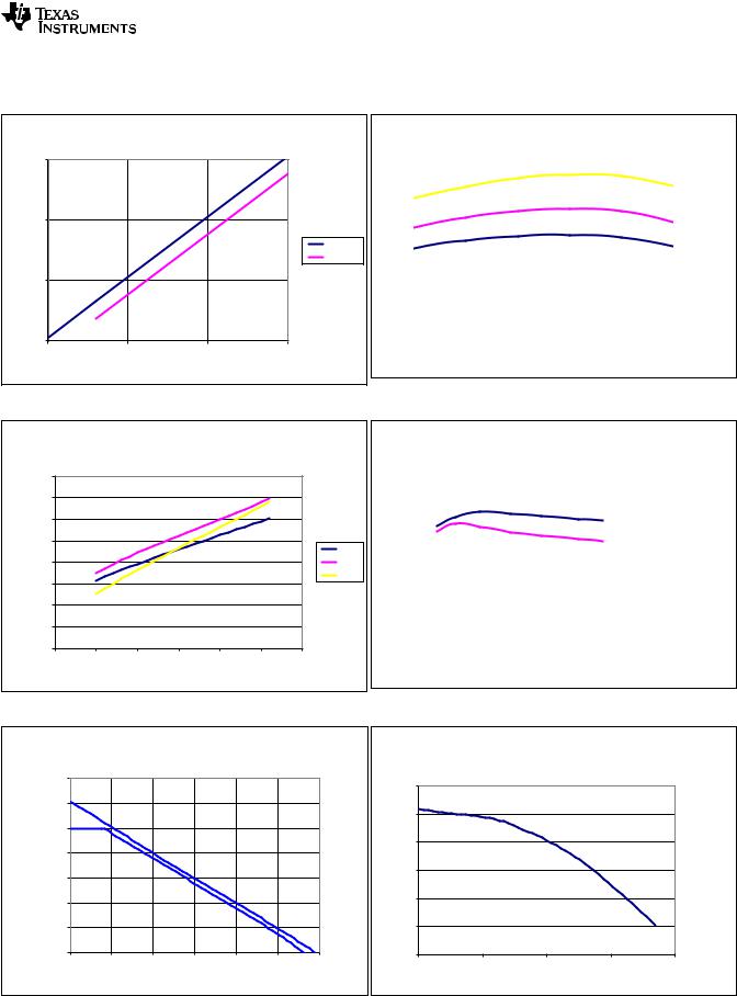
Typical Characteristics
|
|
Input Voltage Range |
|
|
|
15 |
|
|
|
-Vdc) |
|
|
|
|
(+/ |
10 |
|
|
|
Voltage |
|
|
|
Positive |
|
|
|
|
Negative |
Input |
5 |
|
|
|
+/-Vin |
|
|
|
|
|
0 |
|
|
|
|
0 |
5 |
10 |
15 |
|
|
V+ OR V- Power Supply Voltage (+/-Vdc) |
|
|
Figure 3.
Input Current
|
20 |
|
|
|
|
|
|
|
|
|
|
|
|
|
|
|
|
|
|
|
|
|
|
|
|
|
|
|
|
|
|
|
|
|
|
|
|
|
|
|
|
|
|
|
|
|
|
|
18 |
|
|
|
|
|
|
|
|
|
|
|
|
|
|
|
|
|
|
|
|
|
|
|
|
|
|
|
|
|
|
|
|
|
|
|
|
|
|
|
|
|
|
|
|
|
|
(nAdc) |
16 |
|
|
|
|
|
|
|
|
|
|
|
|
|
|
|
|
|
|
|
|
|
|
|
|
|
|
|
|
|
|
|
|
|
|
|
|
|
|
|
|
|
|
|
|
||
14 |
|
|
|
|
|
|
|
|
|
|
|
|
|
|
|
|
|
|
|
|
|
|
|
|
|
|
|
|
|
|
|
|
|
|
|
|
|
|
|
|
|
|
|
|
|
|
|
|
12 |
|
|
|
|
|
|
|
|
|
|
|
|
|
|
|
|
|
|
|
|
|
|
Current |
10 |
|
|
|
|
|
|
|
|
|
|
|
|
|
|
|
|
|
|
|
|
|
5Vdc |
|
|
|
|
|
|
|
|
|
|
|
|
|
|
|
|
|
|
|
|
|
30Vdc |
||
|
|
|
|
|
|
|
|
|
|
|
|
|
|
|
|
|
|
|
|
|
|
15Vdc |
|
Input |
8 |
|
|
|
|
|
|
|
|
|
|
|
|
|
|
|
|
|
|
|
|
|
|
|
|
|
|
|
|
|
|
|
|
|
|
|
|
|
|
|
|
|
|
|
|
||
6 |
|
|
|
|
|
|
|
|
|
|
|
|
|
|
|
|
|
|
|
|
|
|
|
|
|
|
|
|
|
|
|
|
|
|
|
|
|
|
|
|
|
|
|
|
|
||
Ib |
4 |
|
|
|
|
|
|
|
|
|
|
|
|
|
|
|
|
|
|
|
|
|
|
|
|
|
|
|
|
|
|
|
|
|
|
|
|
|
|
|
|
|
|
|
|
|
|
|
2 |
|
|
|
|
|
|
|
|
|
|
|
|
|
|
|
|
|
|
|
|
|
|
|
|
|
|
|
|
|
|
|
|
|
|
|
|
|
|
|
|
|
|
|
|
|
|
|
0 |
|
|
|
|
|
|
|
|
|
|
|
|
|
|
|
|
|
|
|
|
|
|
|
|
|
|
|
|
|
|
|
|
|
|
|
|
|
|
|
|
|
|
|
|
|
|
|
-55 |
-35 |
-15 |
5 |
25 |
45 |
65 |
85 |
105 |
125 |
|
|
|
||||||||||
Ta Temperature (C)
Figure 4.
|
|
|
Supply Current (ICC) |
|
|
|
|
|
0.36 |
|
|
|
|
|
|
|
0.34 |
|
|
|
|
|
|
in mA |
0.32 |
|
|
|
|
|
|
0.3 |
|
|
|
|
|
|
|
Current |
|
|
|
|
|
|
-55C |
0.28 |
|
|
|
|
|
0C |
|
0.26 |
|
|
|
|
|
125C |
|
Supply |
|
|
|
|
|
|
|
0.24 |
|
|
|
|
|
|
|
|
0.22 |
|
|
|
|
|
|
|
0.2 |
|
|
|
|
|
|
|
0 |
5 |
10 |
15 |
20 |
25 |
30 |
|
|
|
|
Supply Voltage |
|
|
|
Figure 5.
Open Loop Frequency Response
|
140 |
|
|
|
|
|
|
|
120 |
|
|
|
|
|
|
(dB) |
100 |
|
|
|
|
|
|
80 |
|
|
|
|
|
|
|
Gain |
|
|
|
|
|
|
|
60 |
|
|
|
|
|
|
|
Voltage |
|
|
|
|
|
|
|
40 |
|
|
|
|
|
|
|
|
20 |
|
|
|
|
|
|
|
0 |
|
|
|
|
|
|
|
1 |
10 |
100 |
1,000 |
10,000 |
100,000 |
1,000,000 |
Frequency (Hz)
Voltage Gain
|
160 |
|
|
|
|
|
|
|
|
|
|
|
|
|
|
|
|
|
|
|
|
|
|
|
|
|
|
|
|
|
|
|
|
|
|
|
|
|
|
|
|
|
140 |
|
|
|
|
|
|
|
|
|
|
|
|
|
|
|
|
|
|
|
|
|
|
|
|
|
|
|
|
|
|
|
|
|
|
|
|
|
|
|
|
(dB) |
120 |
|
|
|
|
|
|
|
|
|
|
|
|
|
|
|
|
|
|
|
|
|
|
|
|
|
|
|
|
|
|
|
|
|
|
|
|
|
|
||
100 |
|
|
|
|
|
|
|
|
|
|
|
|
|
|
|
|
|
|
|
|
Gain |
|
|
|
|
|
|
|
|
|
|
|
|
|
|
|
|
|
|
|
|
|
|
|
|
|
|
|
|
|
|
|
|
|
|
|
|
|
|
|
|
|
Voltage |
80 |
|
|
|
|
|
|
|
|
|
|
|
|
|
|
|
|
|
|
RL=20K |
|
|
|
|
|
|
|
|
|
|
|
|
|
|
|
|
|
|
RL=2K |
||
60 |
|
|
|
|
|
|
|
|
|
|
|
|
|
|
|
|
|
|
||
Avol |
40 |
|
|
|
|
|
|
|
|
|
|
|
|
|
|
|
|
|
|
|
|
|
|
|
|
|
|
|
|
|
|
|
|
|
|
|
|
|
|
||
|
20 |
|
|
|
|
|
|
|
|
|
|
|
|
|
|
|
|
|
|
|
|
|
|
|
|
|
|
|
|
|
|
|
|
|
|
|
|
|
|
|
|
|
0 |
|
|
|
|
|
|
|
|
|
|
|
|
|
|
|
|
|
|
|
|
|
|
|
|
|
|
|
|
|
|
|
|
|
|
|
|
|
|
|
|
|
0 |
5 |
10 |
15 |
20 |
25 |
30 |
35 |
40 |
|
|
|
||||||||
V+ Supply Voltage (Vdc)
Figure 6.
Common Mode Rejection Ratio
(differential gain / common mode gain)
|
120 |
|
|
|
|
|
100 |
|
|
|
|
|
80 |
|
|
|
|
dB |
60 |
|
|
|
|
|
|
|
|
|
|
|
40 |
|
|
|
|
|
20 |
|
|
|
|
|
0 |
|
|
|
|
|
100 |
1,000 |
10,000 |
100,000 |
1,000,000 |
Frequency (Hz)
Figure 7. Min & Max Gain Over Temperature Range |
Figure 8. |
|
|
|
|
Copyright © 1976–2013, Texas Instruments Incorporated |
Submit Documentation Feedback |
9 |
Product Folder Links: LM158 LM258 LM258A LM358 LM358A LM2904 LM2904V

LM158, LM158A, LM258, LM258A
LM358, LM358A, LM2904, LM2904V
SLOS068S –JUNE 1976–REVISED MAY 2013 |
www.ti.com |
Typical Characteristics (continued)
Voltage Follower Pulse Response
|
4 |
|
|
|
|
|
|
|
500 |
|
|
|
|
|
|
|
|
|
450 |
Output Voltage (V) |
3 |
|
|
|
|
|
|
|
|
|
|
|
|
|
|
|
|
400 |
|
2 |
|
|
|
|
|
|
|
|
|
|
|
|
|
|
|
|
|
350 |
|
|
|
|
|
|
|
|
|
(mV)VoltageOutput |
|
Vo |
1 |
|
|
|
|
|
|
|
e0 |
|
|
|
|
|
|
|
|
|
300 |
|
0 |
|
|
|
|
|
|
|
250 |
|
0 |
5 |
10 |
15 |
20 |
25 |
30 |
35 |
40 |
t TIME (uS)
Voltage Follower Pulse Response (Small Signal)
0 |
1 |
2 |
3 |
4 |
5 |
6 |
7 |
8 |
t TIME (uS)
Figure 9. |
Figure 10. |
Large Signal Frequency Response
|
20 |
|
|
|
|
8 |
|
|
|
|
|
|
|
|
17.5 |
|
|
|
Vcc |
7 |
|
|
|
|
|
||
|
|
|
|
|
to |
|
|
15 |
|
|
|
|
|
(Vp-p) |
|
|
|
relative |
6 |
|
|
|
|
|
|||
12.5 |
|
|
|
|
||
Swing |
|
|
|
|
(Vdc) |
5 |
10 |
|
|
|
|
||
|
|
|
|
|
||
Output |
|
|
|
|
Voltage |
4 |
7.5 |
|
|
|
|
||
|
|
|
|
3 |
||
Vo |
5 |
|
|
|
Output |
|
|
|
|
|
|||
2.5 |
|
|
|
2 |
||
|
|
|
|
Vo |
|
|
|
|
|
|
|
1 |
|
|
0 |
|
|
|
|
|
|
|
|
|
|
0.001 |
|
|
1 |
10 |
100 |
1000 |
|
|
|
|
|
f Frequency (kHz)
Output Characteristics Current Sourcing
0.01 |
0.1 |
1 |
10 |
100 |
Io Output Sink Current (mAdc)
Figure 11. |
Figure 12. |
|
|
Output Characteristics Current Sinking |
|
|||
|
10 |
|
|
|
|
|
(Vdc) |
1 |
|
|
|
|
|
Voltage |
|
|
|
|
|
5Vdc |
|
|
|
|
|
15Vdc |
|
|
|
|
|
|
|
|
Output |
|
|
|
|
|
30Vdc |
0.1 |
|
|
|
|
|
|
|
|
|
|
|
|
|
Vo |
|
|
|
|
|
|
|
0.01 |
|
|
|
|
|
|
0.001 |
0.01 |
0.1 |
1 |
10 |
100 |
|
|
Io Output Sink Current (mAdc) |
|
|
||
Figure 13.
Current Limiting
|
90 |
|
|
|
|
|
|
|
|
|
|
80 |
|
|
|
|
|
|
|
|
|
(mAdc) |
70 |
|
|
|
|
|
|
|
|
|
60 |
|
|
|
|
|
|
|
|
|
|
|
|
|
|
|
|
|
|
|
|
|
Current |
50 |
|
|
|
|
|
|
|
|
|
40 |
|
|
|
|
|
|
|
|
|
|
Output |
|
|
|
|
|
|
|
|
|
|
30 |
|
|
|
|
|
|
|
|
|
|
|
|
|
|
|
|
|
|
|
|
|
Io+ |
20 |
|
|
|
|
|
|
|
|
|
|
|
|
|
|
|
|
|
|
|
|
|
10 |
|
|
|
|
|
|
|
|
|
|
0 |
|
|
|
|
|
|
|
|
|
|
-55 |
-35 |
-15 |
5 |
25 |
45 |
65 |
85 |
105 |
125 |
|
|
|
|
|
Ta Temperature |
|
|
|
|
|
Figure 14.
10 |
Submit Documentation Feedback |
Copyright © 1976–2013, Texas Instruments Incorporated |
Product Folder Links: LM158 LM258 LM258A LM358 LM358A LM2904 LM2904V
LM158, LM158A, LM258, LM258A
LM358, LM358A, LM2904, LM2904V
www.ti.com |
SLOS068S –JUNE 1976–REVISED MAY 2013 |
Typical Characteristics (continued)
|
|
|
Input Current (LM2902 Only) |
|
|
|
|
|
|
Voltage Gain (LM2902 Only) |
|
|
|||
|
|
|
|
|
|
|
|
|
|
|
|
|
|
||
|
50.00 |
|
|
|
|
|
|
|
160 |
|
|
|
|
|
|
|
|
|
|
|
|
|
|
|
|
|
|
|
|
|
|
|
|
|
|
|
|
|
|
|
140 |
|
|
|
|
|
|
(nAdc)CurrentInputIin |
37.50 |
|
|
|
|
|
|
GainVoltageAvol(dB) |
120 |
|
|
|
|
|
|
|
|
|
|
|
|
|
|
|
|
|
|
|
|||
|
|
|
|
|
|
|
100 |
|
|
|
|
|
|
||
|
|
|
|
|
|
|
|
|
|
|
|
|
|
|
|
|
25.00 |
|
|
|
|
|
|
|
80 |
|
|
|
|
|
RL=20K |
|
|
|
|
|
|
|
|
|
|
|
|
|
RL=2K |
||
|
|
|
|
|
|
|
|
|
|
|
|
|
|
|
|
|
|
|
|
|
|
|
|
|
60 |
|
|
|
|
|
|
|
12.50 |
|
|
|
|
|
|
|
40 |
|
|
|
|
|
|
|
|
|
|
|
|
|
|
|
20 |
|
|
|
|
|
|
|
0.00 |
|
|
|
|
|
|
|
0 |
|
|
|
|
|
|
|
0 |
5 |
10 |
15 |
20 |
25 |
30 |
|
0 |
5 |
10 |
15 |
20 |
25 |
30 |
|
|
|
V+ Supply Voltage (Vdc) |
|
|
|
|
|
V+ Supply Voltage (Vdc) |
|
|
||||
Figure 15. |
Figure 16. |
Copyright © 1976–2013, Texas Instruments Incorporated |
Submit Documentation Feedback |
11 |
Product Folder Links: LM158 LM258 LM258A LM358 LM358A LM2904 LM2904V
Loading...