


SGS Thomson Microelectronics HCF4077BM1, HCF4077BF, HCF4077BEY, HCF4077BC1, HCF4077B Datasheet
...4070B±QUAD EXCLUSIVE±OR GATE
.4037B±QUAD EXCLUSIVE±NOR GATE
MEDIUM-SPEED OPERATION tPHL = tPLH =
.70ns (typ.) AT VCC = 10V, CL = 50pF QUIESCENT CURRENT SPECIFIED TO 20V
.FOR HCC DEVICE
.5V, 10V AND 15V PARAMETRIC RATING INPUT CURRENT OF 100nA AT 18V AND
.25°C FOR HCC DEVICE
.100% TESTED FOR QUIESCENT CURRENT MEETS ALL REQUIREMENTS OF JEDECTENTATIVE STANDARD No. 13A, ºSTANDARD SPECIFICATIONS FOR DESCRIPTION OF ºBº SERIES CMOS DEVICESº
HCC4070/77B
HCF4070/77B
GATES
EY |
F |
(Plastic Package) |
(Ceramic Package) |
M1 |
C1 |
(Micro Package) |
(Chip Carrier) |
ORDER CODES :
HCC40XXBF HCF40XXBM1 HCF40XXBEY HCF40XXBC1
DESCRIPTION
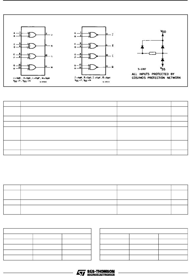
The HCC4070B/4077B (extended temperature range) and HCF4070B/4077B (intermediate temperature range) are monolithic integrated circuits, available in 14-lead dual in-line plastic or ceramic package and plastic micropackage.
The HCC/HCF4070B contains four independent ex- clusive-OR gates.
The HCC/HCF4077B contains four independent ex- clusive-NOR gates.
The HCC/HCF4070B and HCC/HCF4077B provide the system designer with a means for direct implementation of the exclusive-OR and exclusiveNOR function, respectively. For applications as Logical comparators, Adders/subtractors, Parity generators and checkers.
PIN CONNECTIONS
4070B
4077B
September 1988 |
1/11 |
HCC/HCF4070B/4077B
FUNCTIONAL DIAGRAM
4070B |
4077B |
ABSOLUTE MAXIMUM RATING
Symbol |
Parameter |
Value |
Unit |
VDD * |
Supply Voltage: HCC Types |
-0.5 to +20 |
V |
|
HCF Types |
-0.5 to +18 |
V |
Vi |
Input Voltage |
-0.5 to VDD + 0.5 |
V |
II |
DC Input Current (any one input) |
± 10 |
mA |
Ptot |
Total Power Dissipation (per package) |
200 |
mW |
|
Dissipation per Output Transistor |
|
|
|
for Top = Full Package Temperature Range |
100 |
mW |
Top |
Operating Temperature: HCC Types |
-55 to +125 |
oC |
|
HCF Types |
-40 to +85 |
oC |
Tstg |
Storage Temperature |
-65 to +150 |
oC |
Stresses above those listed under ºAbsolute Maximum Ratingsº may cause permanent damage to the device. This is a stress ratingonly and functional operation of the device at these or any other conditions above those indicated in the operational sections of this specification is not implied. Exposure to absolute maximum rating conditions for external periods may affect device reliability.
* All voltage values are referred to VSS pin voltage.
RECOMMENDED OPERATING CONDITIONS
Symbol |
Parameter |
Value |
Unit |
VDD |
Supply Voltage: HCC Types |
3 to 18 |
V |
|
HCF Types |
3 to 15 |
V |
VI |
Input Voltage |
0 to VDD |
V |
Top |
Operating Temperature: HCC Types |
-55 to +125 |
oC |
|
HCF Types |
-40 to +85 |
oC |
TRUTH TABLES (1 of 4 gates)
|
HCC4070B |
|
|
HCC4077B |
|
A |
B |
J |
A |
B |
J |
0 |
0 |
0 |
0 |
0 |
1 |
1 |
0 |
1 |
1 |
0 |
0 |
0 |
1 |
1 |
0 |
1 |
0 |
1 |
1 |
0 |
1 |
1 |
1 |
2/11
HCC/HCF4070B/4077B
STATIC ELECTRICAL CHARACTERISTICS (over recommended operating conditions)
Test Conditios |
Value |
Symbol
IL
VOH
VOL
VIH
VIL
IOL
IOL
IIH, IIL
CI
Parameter |
VI |
VO |
|IO| |
VDD |
TLOW * |
|
25 oC |
|
THIGH * |
Unit |
|
|
|
(V) |
(V) |
(μA) |
(V) |
Min. Max. |
Min. Typ. |
Max. Min. Max. |
|
||
Quiescent |
|
0/5 |
|
|
5 |
1 |
|
0.02 |
1 |
30 |
|
Current |
HCC |
0/10 |
|
|
10 |
2 |
|
0.02 |
2 |
60 |
|
|
Types |
|
|
|
|
||||||
|
0/15 |
|
|
15 |
4 |
|
0.02 |
4 |
120 |
|
|
|
|
|
|
|
μA |
||||||
|
|
0/20 |
|
|
20 |
20 |
|
0.04 |
20 |
600 |
|
|
|
|
|
|
|
||||||
|
HCF |
0/5 |
|
|
5 |
4 |
|
0.02 |
4 |
30 |
|
|
0/10 |
|
|
10 |
8 |
|
0.02 |
8 |
60 |
|
|
|
Types |
|
|
|
|
||||||
|
|
|
|
|
|
|
|
|
|
|
|
|
|
0/15 |
|
|
15 |
16 |
|
0.02 |
16 |
120 |
|
Output High |
|
0/5 |
|
< 1 |
5 |
4.95 |
4.95 |
|
|
4.95 |
|
Voltage |
|
0/10 |
|
< 1 |
10 |
9.95 |
9.95 |
|
|
9.95 |
V |
|
|
|
|
|
|
||||||
|
|
0/15 |
|
< 1 |
15 |
14.95 |
14.95 |
|
|
14.95 |
|
Output Low |
|
5/0 |
|
< 1 |
5 |
0.05 |
|
|
0.05 |
0.05 |
|
Voltage |
|
10/0 |
|
< 1 |
10 |
0.05 |
|
|
0.05 |
0.05 |
V |
|
|
|
|
|
|
||||||
|
|
15/0 |
|
< 1 |
15 |
0.05 |
|
|
0.05 |
0.05 |
|
Input High |
|
|
0.5/4.5 |
< 1 |
5 |
3.5 |
3.5 |
|
|
3.5 |
|
Voltage |
|
|
1/9 |
< 1 |
10 |
7 |
7 |
|
|
7 |
V |
|
|
|
|
|
|
||||||
|
|
|
1.5/13.5 |
< 1 |
15 |
11 |
11 |
|
|
11 |
|
Input Low |
|
|
4.5/0.5 |
< 1 |
5 |
1.5 |
|
|
1.5 |
1.5 |
|
Voltage |
|
|
9/1 |
< 1 |
10 |
3 |
|
|
3 |
3 |
V |
|
|
|
|
|
|
||||||
|
|
|
13.5/1.5 |
< 1 |
15 |
4 |
|
|
4 |
4 |
|
Output |
|
0/5 |
2.5 |
|
5 |
-2 |
-1.6 |
-3.2 |
|
-1.15 |
|
Drive |
HCC |
0/5 |
4.6 |
|
5 |
-0.64 |
-0.51 |
-1 |
|
-0.36 |
|
Current |
Types |
|
|
|
|||||||
0/10 |
9.5 |
|
10 |
-1.6 |
-1.3 |
-2.6 |
|
-0.9 |
|
||
|
|
|
|
|
|||||||
|
|
0/15 |
13.5 |
|
15 |
-4.2 |
-3.4 |
-6.8 |
|
-2.4 |
mA |
|
|
0/5 |
2.5 |
|
5 |
-1.53 |
-1.36 |
-3.2 |
|
-1.1 |
|
|
HCF |
0/5 |
4.6 |
|
5 |
-0.52 |
-0.44 |
-1 |
|
-0.36 |
|
|
Types |
|
|
|
|||||||
|
0/10 |
9.5 |
|
10 |
-1.3 |
-1.1 |
-2.6 |
|
-0.9 |
|
|
|
|
|
|
|
|||||||
|
|
0/15 |
13.5 |
|
15 |
-3.6 |
-3.0 |
-6.8 |
|
-2.4 |
|
Output |
HCC |
0/5 |
0.4 |
|
5 |
0.64 |
0.51 |
1 |
|
0.36 |
|
Sink |
0/10 |
0.5 |
|
10 |
1.6 |
1.3 |
2.6 |
|
0.9 |
|
|
Types |
|
|
|
||||||||
Current |
|
|
|
||||||||
|
|
|
|
|
|
|
|
|
|
||
|
0/15 |
1.5 |
|
15 |
4.2 |
3.4 |
6.8 |
|
2.4 |
mA |
|
|
|
|
|
||||||||
|
HCF |
0/5 |
0.4 |
|
5 |
0.52 |
0.44 |
1 |
|
0.36 |
|
|
0/10 |
0.5 |
|
10 |
1.3 |
1.1 |
2.6 |
|
0.9 |
|
|
|
Types |
|
|
|
|||||||
|
|
|
|
|
|
|
|
|
|
|
|
|
|
0/15 |
1.5 |
|
15 |
3.6 |
3.0 |
6.8 |
|
2.4 |
|
Input |
HCC |
0/18 |
|
|
18 |
±0.1 |
|
±10-5 |
±0.1 |
±1 |
|
Leakage |
Types |
|
Any Input |
|
|
|
|
|
|
μA |
|
Current |
HCF |
|
|
|
|
|
|
|
|||
0/15 |
|
|
15 |
±0.3 |
|
±10-5 |
±0.3 |
±1 |
|
||
|
|
|
|
|
|||||||
|
Types |
|
|
|
|
|
|
|
|
|
|
Input Capacitance |
|
Any Input |
|
|
|
5 |
7.5 |
|
pF |
||
*TLOW = -55 oC for HCC device: -40 oC for HCF device.
*THIGH = +125 oC for HCC device: +85 oC for HCF device.
The Noise Margin for both º1º and º0º level is: 1V min. with V DD = 5 V, 2 V min. with VDD = 10 V, 2.5 V min. with VDD = 15 V
3/11

HCC/HCF4070B/4077B
DYNAMIC ELECTRICAL CHARACTERISTICS (Tamb = 25 oC, CL = 50 pF, RL = 200 KΩ, typical temperature coefficent for all VDD values is 03 %/oC, all input rise and fall times= 20 ns)
Symbol |
Parameter |
Test Conditions |
Value |
|
Unit |
|
VDD (V) Min. |
Typ. |
Max. |
||||
|
|
|
||||
tPLH |
Propagation Delay Time |
5 |
140 |
280 |
|
|
tPHL |
|
10 |
65 |
130 |
ns |
|
|
|
15 |
50 |
100 |
|
|
tTLH |
Transition Time |
5 |
100 |
200 |
|
|
tTHL |
|
10 |
50 |
100 |
ns |
|
|
|
15 |
40 |
80 |
|
Minimum Output High (source) Current Characteristics.
Minimum Output Low (sink) Current Characteristics.
Typical Output Low (sink) Current.
Typical Output High (source) Current Characteristics.
4/11
 Loading...