


SGS Thomson Microelectronics L4892CX, L4812CX, L4808CX, L4808CV, L4805CX Datasheet
...L4805-L4885-L4892
L4808-L4810-L4812
VERY LOW DROP VOLTAGE REGULATORS
.
.INPUT/OUTPUT DROP TYP. 0.4V
.400mA OUTPUT CURRENT
.LOW QUIESCENT CURRENT
.REVERSE POLARITY PROTECTION
.OVERVOLTAGE PROTECTION (± 60V)
.FOLDBACK CURRENT LIMITING THERMAL SHUTDOWN
DESCRIPTION
L4800 series devices are voltage regulators with a very low voltage drop (typically 0.4V at full rated current), output current up to 400mA, low quiescent current and comprehensiveon-chip protection.These devices are protected against load dump and field decay transients of ± 60V, polarity reversal and overheating. A foldback current limiter protects against load short circuits. Available in 5V, 8.5V, 9.2V,10V and12V versions (all± 4%, TI = 25°C) these regulators are designed for automotive, industrial and consumer applications where low consumption is particularly important.
SO T-82 |
TO-220 |
In automotive applications the L4805 is ideal for 5V logic supplies becauseit can operateeven when the batteryvoltage falls below 6V. In batterybackup and standby applications the low consumption of these devices extends battery life.
BLOCK DIAGRAM
March 1992 |
1/7 |
L4805-L4808-L4885-L4892-L4810-L4812
ABSOLUTE MAXIMUM RATINGS
Symbol |
Parameter |
VI |
DC Input Voltage |
|
DC Input Reverse Voltage |
|
Transient Input Overvoltages : |
|
Load Dump : |
|
5ms < Trise < 10ms, |
|
τf Fall Time Constant = 100ms, |
|
Rsource < 0.5Ω |
|
Field Decay : |
|
5ms < tfall < 10ms, Rsource < 10Ω |
|
τr Rise Time Constant = 33ms |
Tj, Tstg |
Junction and Storage Temperature Range |
THERMAL DATA
Symbol |
Parameter |
Rth j-case |
Thermal Resistance Junction-case |
Rth j-amb |
Thermal Resistance Junction-ambient |
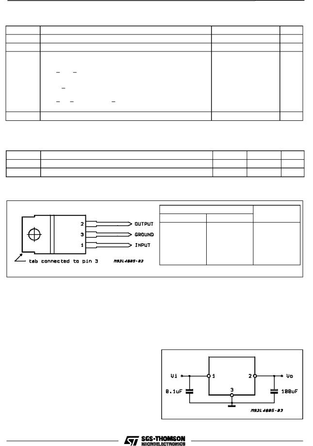
PIN CONNECTION (top view)
TEST AND APPLICATION CIRCUIT
The output capacitor is required for stability. Though the 100 μF shown is the minimum recommended value, actual size and type may vary depending upon the application load and temperature range. Capacitor effectiveseries resistance (ESR) also factors in the IC stability. Since ESR varies from one brandto the next,some bench work may be required to determine the minimum capacitor value to use in production. Worst-case is usually determined at the minimum ambient temperature and maximum load expected.
Output capacitors can be increased in size to any desired value above the minimum. One possible purpose of this would be to maintain the output voltages during brief conditions of negative input transients that might be characteristics of a particular system.
Value |
Unit |
+ 35 |
V |
- 18 |
V |
60 |
V |
- 60 |
V |
- 55 to + 150 |
°C |
|
SOT82 |
TO220 |
Unit |
|
Max. |
8 |
4 |
°C/W |
|
Max. |
100 |
75 |
°C/W |
|
Order Codes |
Output Voltage |
|||
TO-220 |
SOT-82 |
|||
|
|
|||
L4805CV |
L4805CX |
5V |
|
|
L4808CV |
L4808CX |
8V |
|
|
L4885CV |
L4885CX |
8.5 V |
|
|
L4892CV |
L4892CX |
9.2 V |
|
|
L4810CV |
L4810CX |
10 V |
|
|
L4812CV |
L4812CX |
12 V |
|
|
Capacitors must also be rated at all ambient temperature expected in the system. Many aluminum type electrolytics will freeze at temperatures less than ± 30 °C, reducing their effective capacitance to zero. To maintain regulator stability down to ± 40 °C, capacitors rated at that temperature (such as tantalums) must be used.
2/7

L4805-L4808-L4885-L4892-L4810-L4812
ELECTRICAL CHARACTERISTICS (VI = 14.4V; CO = 100μF; Tj = 25°C unless otherwise specified.)
Symbol |
Parameter |
T est Con di tio n |
Min. Typ. Max. Uni t |
|||
VO |
Output Voltage |
IO = 5mA to 400mA (L4805) |
4.80 |
5.00 |
5.20 |
V |
|
|
IO = 5mA to 400mA (L4808) |
7.68 |
8.00 |
8.32 |
V |
|
|
IO = 5mA to 400mA (L4810) |
8.16 |
8.50 |
8.84 |
V |
|
|
IO = 5mA to 400mA (L4812) |
8.83 |
9.20 |
9.57 |
V |
|
|
IO = 5mA to 400mA (L4885) |
9.60 |
10.00 |
10.40 |
V |
|
|
IO = 300mA (L4892) |
11.50 |
12.00 |
12.50 |
V |
VI |
Operating Input Voltage |
|
|
|
26 |
V |
VO/VO |
Line Regulation |
VI = 13 to 26V; IO = 5mA |
|
1 |
10 |
mV/V |
VO/VO |
Load Regulation |
IO = 5 to 400mA* |
|
3 |
15 |
mV/V |
VI - VO |
Dropout Voltage |
IO = 400mA* |
|
0.4 |
0.7 |
V |
|
|
IO = 150mA |
|
0.2 |
0.4 |
V |
Iq |
Quiescent Current |
IO = 0mA |
|
0.8 |
2 |
mA |
|
|
IO = 150mA |
|
25 |
45 |
mA |
|
|
IO = 400mA* |
|
65 |
90 |
mA |
VO |
Temperature Output Voltage |
|
|
0.1 |
|
mV |
• |
Drift |
|
|
|
|
° • |
T VO |
|
|
|
|
|
C V |
SVR |
Supply Voltage Rejection |
IO = 350mA; f = 320Hz; |
|
60 |
|
dB |
|
CO = 100μF; VI = VO +3V+2Vpp |
|
|
|
|
|
|
|
|
|
|
|
|
IO |
Max Output Current |
|
|
800 |
|
mA |
ISC |
Output Short Circuit Current |
|
|
350 |
500 |
mA |
|
(fold back condition) |
|
|
|
|
|
* only for L4892 the current test conditions is IO = 300mA
ELECTRICAL CHARACTERISTICS (VI = 14.4V; CO = 100μF; Tj = -40 to 125°C (note 1) unless otherwise specified.)
Symbol |
Parameter |
T est Con di tio n |
Min. Typ. Max. Uni t |
|||
VO |
Output Voltage |
IO = 5mA to 400mA (L4805) |
4.70 |
5.00 |
5.30 |
V |
|
|
IO = 5mA to 400mA (L4808) |
7.50 |
8.00 |
8.50 |
V |
|
|
IO = 5mA to 400mA (L4810) |
8.00 |
8.50 |
9.00 |
V |
|
|
IO = 5mA to 400mA (L4812) |
8.65 |
9.20 |
9.75 |
V |
|
|
IO = 5mA to 400mA (L4885) |
9.40 |
10.00 |
10.60 |
V |
|
|
IO = 300mA (L4892) |
11.30 |
12.00 |
12.70 |
V |
VI |
Operating Input Voltage |
see note 2 |
|
|
26 |
V |
VO/VO |
Line Regulation |
VI = 14 to 26V; IO = 5mA |
|
2 |
15 |
mV/V |
VO/VO |
Load Regulation |
IO = 5 to 400mA* |
|
5 |
25 |
mV/V |
VI - VO |
Dropout Voltage |
IO = 400mA* |
|
0.5 |
0.9 |
V |
|
|
IO = 150mA |
|
0.25 |
0.5 |
V |
Iq |
Quiescent Current |
IO = 0mA |
|
1.2 |
3 |
mA |
|
|
IO = 150mA |
|
40 |
70 |
mA |
|
|
IO = 400mA* |
|
80 |
140 |
mA |
IO |
Max Output Current |
|
|
870 |
|
mA |
ISC |
Output Short Circuit Current |
|
|
230 |
|
mA |
|
(fold back condition) |
|
|
|
|
|
Notes : 1. This limits are guaranteed by design, correlation and statistical control on production samples over the indicated temperature and supply voltage ranges..
2. For a DC voltage 26V < Vi < 35V the device is not operating.
3/7
 Loading...