


SGS Thomson Microelectronics L7952ACV, L7952ACD2T, L7924ACV, L7924ACD2T, L7922ACV Datasheet
...
|
L7900AC |
|
SERIES |
|
2% NEGATIVE VOLTAGE REGULATORS |
■OUTPUT CURRENT UP TO 1.5 A
■OUTPUT VOLTAGES OF -5; -5.2; -6; -8; -12; -15; -18; -20; -22; -24V
■THERMAL OVERLOAD PROTECTION
■SHORT CIRCUIT PROTECTION
■OUTPUT TRANSITION SOA PROTECTION
DESCRIPTION
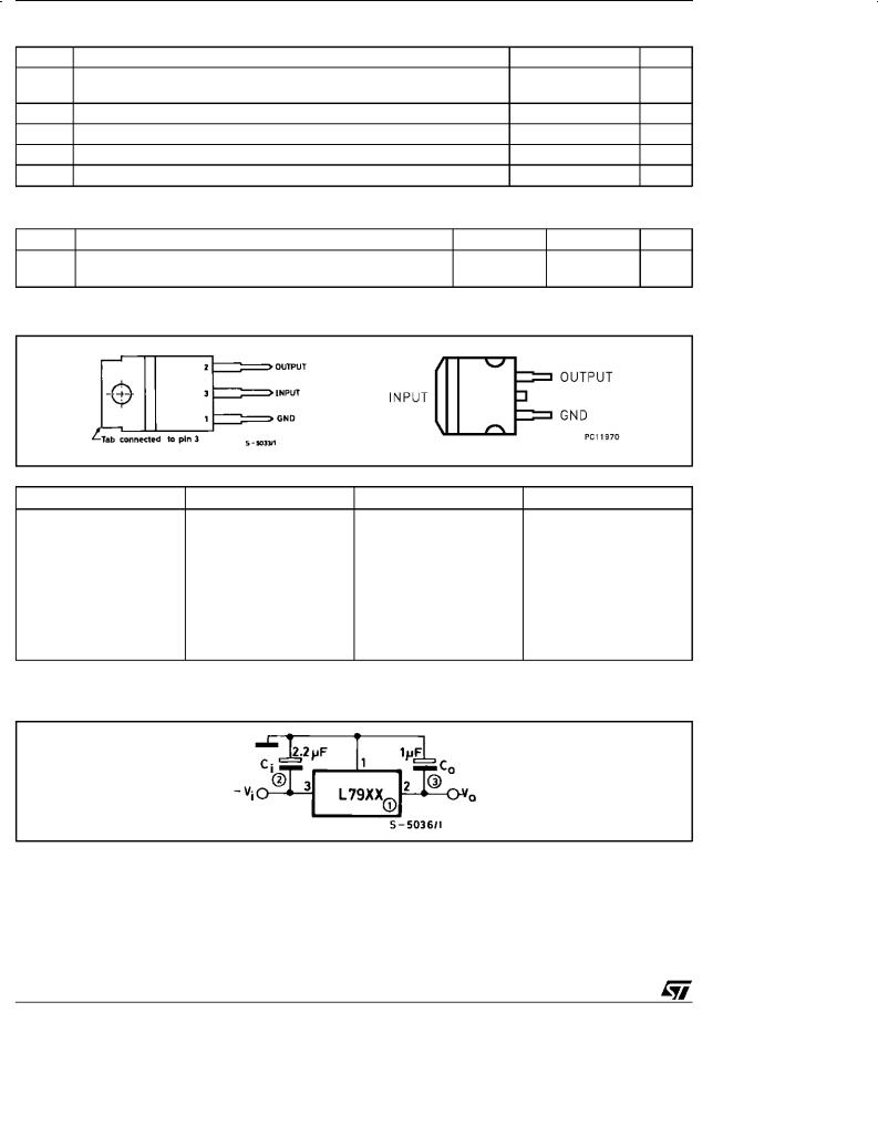
The L7900AC series of three-terminal negative regulators is available in TO-220 and D2PAK packages and several fixed output voltages. These regulators can provide local on-card regulation, eliminating the distribution problems associated with single point regulation; furthermore, having the same voltage option as the L7800A positive standard series, they are particularly suited for split power supplies. In addition, the -5.2V is also available for ECL system. If adequate heat sinking is provided, they can deliver over 1.5A output current. Although designed primarily as fixed voltage regulators, these devices can be used with external components to obtain adjustable voltages and currents.
3
1
D2PAK
TO-220
SCHEMATIC DIAGRAM
November 1999 |
1/11 |
L7900AC
ABSOLUTE MAXIMUM RATINGS
Symbol |
Parameter |
Value |
Unit |
|
Vi |
DC Input Voltage (for VO = -5 to -18V) |
-35 |
|
V |
|
(for VO = -20, -24V) |
-40 |
|
V |
Io |
Output Current |
Internally |
limited |
|
Ptot |
Power Dissipation |
Internally |
limited |
|
Top |
Operating Junction Temperature Range |
0 to 125 |
o C |
|
Tst g |
Storage Temperature Range |
- 65 to |
150 |
o C |
THERMAL DATA
Symbol |
Parameter |
|
D2PAK |
TO-220 |
Unit |
Rthjca se |
Thermal Resistance Junction-case |
Max |
3 |
3 |
oC/W |
Rthjamb |
Thermal Resistance Junction-ambient |
Max |
62.5 |
50 |
oC/W |
CONNECTION DIAGRAM AND ORDERING NUMBERS (top view)
|
TO-220 |
|
D2PAK |
Type |
TO-220 |
D2PAK (*) |
Output Voltage |
L7905AC |
L7905ACV |
L7905ACD2T |
-5V |
L7952AC |
L7952ACV |
L7952ACD2T |
-5.2V |
L7906AC |
L7906ACV |
L7906ACD2T |
-6V |
L7908AC |
L7908ACV |
L7908ACD2T |
-8V |
L7912AC |
L7912ACV |
L7912ACD2T |
-12V |
L7915AC |
L7915ACV |
L7915ACD2T |
-15V |
L7918AC |
L7918ACV |
L7918ACD2T |
-18V |
L7920AC |
L7920ACV |
L7920ACD2T |
-20V |
L7922AC |
L7922ACV |
L7922ACD2T |
-22V |
L7924AC |
L7924ACV |
L7924ACD2T |
-24V |
(*) AVAILABLE IN TAPE AND REEL WITH º-TRº SUFFIX
APPLICATION CIRCUIT
2/11
L7900AC
ELECTRICAL CHARACTERISTICS FOR L7905A (refer to the test circuits, Tj = 0 to 125 oC, Vi = -10V, Io = 500 mA, Ci = 2.2 μF, Co = 1 μF unless otherwise specified)
Symbol |
Parameter |
|
Test Conditions |
Min. |
Typ. |
Max. |
Unit |
|
Vo |
Output Voltage |
Tj = 25 oC |
|
|
-4.9 |
-5 |
-5.1 |
V |
Vo |
Output Voltage |
Io = -5 mA to -1 A |
Po ≤ 15 W |
-4.8 |
-5 |
-5.2 |
V |
|
|
|
Vi = 8 to 20 V |
|
|
|
|
|
|
Vo* |
Line Regulation |
Vi = -7 to -25 V Tj = 25 oC |
|
|
100 |
mV |
||
|
|
Vi = -8 to -12 V Tj = 25 oC |
|
|
50 |
mV |
||
Vo* |
Load Regulation |
Io = 5 to 1500 mA |
Tj = 25 oC |
|
|
100 |
mV |
|
|
|
Io = 250 to 750 mA |
Tj = 25 oC |
|
|
50 |
mV |
|
Id |
Quiescent Current |
Tj = 25 oC |
|
|
|
|
3 |
mA |
Id |
Quiescent Current Change |
Io = 5 to 1000 mA |
|
|
|
0.5 |
mA |
|
Id |
Quiescent Current Change |
Vi = -8 to -25 V |
|
|
|
1.3 |
mA |
|
Vo |
Output Voltage Drift |
Io = 5 mA |
|
|
|
-0.4 |
|
mV/oC |
T |
|
|
|
|
|
|
|
|
eN |
Output Noise Voltage |
B = 10Hz to 100KHz Tj = 25 oC |
|
100 |
|
μV |
||
SVR |
Supply Voltage Rejection |
Vi = 10 V |
f = 120 Hz |
54 |
60 |
|
dB |
|
Vd |
Dropout Voltage |
Io = 1 A |
Tj = 25 oC |
|
1.4 |
|
V |
|
|
|
VO = 100 mV |
|
|
|
|
|
|
Is c |
Short Circuit Current |
|
|
|
|
2.1 |
|
A |
Iscp |
Short Circuit Peak Current |
Tj = 25 oC |
|
|
|
2.5 |
|
A |
ELECTRICAL CHARACTERISTICS FOR L7952A (refer to the test circuits, Tj = 0 to 125 oC, Vi = -10V, Io = 500 mA, Ci = 2.2 μF, Co = 1 μF unless otherwise specified)
Symbol |
Parameter |
|
Test Conditions |
Min. |
Typ. |
Max. |
Unit |
|
Vo |
Output Voltage |
Tj = 25 oC |
|
|
-5.1 |
-5.2 |
-5.3 |
V |
Vo |
Output Voltage |
Io = -5 mA to -1 A |
Po ≤ 15 W |
-5 |
-5.2 |
-5.4 |
V |
|
|
|
Vi = -9 to -21 V |
|
|
|
|
|
|
Vo* |
Line Regulation |
Vi = -8 to -25 V Tj = 25 oC |
|
|
105 |
mV |
||
|
|
Vi = -9 to -13 V Tj = 25 oC |
|
|
52 |
mV |
||
Vo* |
Load Regulation |
Io = 5 to 1500 mA |
Tj = 25 oC |
|
|
105 |
mV |
|
|
|
Io = 250 to 750 mA |
Tj = 25 oC |
|
|
52 |
mV |
|
Id |
Quiescent Current |
Tj = 25 oC |
|
|
|
|
3 |
mA |
Id |
Quiescent Current Change |
Io = 5 to 1000 mA |
|
|
|
0.5 |
mA |
|
Id |
Quiescent Current Change |
Vi = -9 to -25 V |
|
|
|
1.3 |
mA |
|
Vo |
Output Voltage Drift |
Io = 5 mA |
|
|
|
-0.5 |
|
mV/oC |
T |
|
|
|
|
|
|
|
|
eN |
Output Noise Voltage |
B = 10Hz to 100KHz Tj = 25 oC |
|
125 |
|
μV |
||
SVR |
Supply Voltage Rejection |
Vi = 10 V |
f = 120 Hz |
54 |
60 |
|
dB |
|
Vd |
Dropout Voltage |
Io = 1 A |
Tj = 25 oC |
|
1.4 |
|
V |
|
|
|
VO = 100 mV |
|
|
|
|
|
|
Is c |
Short Circuit Current |
|
|
|
|
2.1 |
|
A |
Iscp |
Short Circuit Peak Current |
Tj = 25 oC |
|
|
|
2.5 |
|
A |
* Load and line regulation are specified at constant junction temperature. Changes in Vo due to heating effects must be taken into account separately. Pulce testing with low duty cycle is used.
3/11

L7900AC
ELECTRICAL CHARACTERISTICS FOR L7906A (refer to the test circuits, Tj = 0 to 125 oC, Vi = -11V, Io = 500 mA, Ci = 2.2 μF, Co = 1 μF unless otherwise specified)
Symbol |
Parameter |
|
Test Conditions |
Min. |
Typ. |
Max. |
Unit |
|
Vo |
Output Voltage |
Tj = 25 oC |
|
|
-5.88 |
-6 |
-6.12 |
V |
Vo |
Output Voltage |
Io = -5 mA to -1 A |
Po ≤ 15 W |
-5.76 |
-6 |
-6.24 |
V |
|
|
|
Vi = -9.5 to -21.5 V |
|
|
|
|
|
|
Vo* |
Line Regulation |
Vi = -8.5 to -25 V |
Tj = 25 oC |
|
|
120 |
mV |
|
|
|
Vi = -9 to -15 V Tj = 25 oC |
|
|
60 |
mV |
||
Vo* |
Load Regulation |
Io = 5 to 1500 mA |
Tj = 25 oC |
|
|
120 |
mV |
|
|
|
Io = 250 to 750 mA |
Tj = 25 oC |
|
|
60 |
mV |
|
Id |
Quiescent Current |
Tj = 25 oC |
|
|
|
|
3 |
mA |
Id |
Quiescent Current Change |
Io = 5 to 1000 mA |
|
|
|
0.5 |
mA |
|
Id |
Quiescent Current Change |
Vi = -9.5 to -25 V |
|
|
|
1.3 |
mA |
|
Vo |
Output Voltage Drift |
Io = 5 mA |
|
|
|
-0.6 |
|
mV/oC |
T |
|
|
|
|
|
|
|
|
eN |
Output Noise Voltage |
B = 10Hz to 100KHz Tj = 25 oC |
|
144 |
|
μV |
||
SVR |
Supply Voltage Rejection |
Vi = 10 V |
f = 120 Hz |
54 |
60 |
|
dB |
|
Vd |
Dropout Voltage |
Io = 1 A |
Tj = 25 oC |
|
1.4 |
|
V |
|
|
|
VO = 100 mV |
|
|
|
|
|
|
Is c |
Short Circuit Current |
|
|
|
|
2 |
|
A |
Iscp |
Short Circuit Peak Current |
Tj = 25 oC |
|
|
|
2.5 |
|
A |
ELECTRICAL CHARACTERISTICS FOR L7908A (refer to the test circuits, Tj = 0 to 125 oC, Vi = -14V, Io = 500 mA, Ci = 2.2 μF, Co = 1 μF unless otherwise specified)
Symbol |
Parameter |
|
Test Conditions |
Min. |
Typ. |
Max. |
Unit |
|
Vo |
Output Voltage |
Tj = 25 oC |
|
|
-7.84 |
-8 |
-8.16 |
V |
Vo |
Output Voltage |
Io = -5 mA to -1 A |
Po ≤ 15 W |
-7.68 |
-8 |
-8.32 |
V |
|
|
|
Vi = -11.5 to -23 V |
|
|
|
|
|
|
Vo* |
Line Regulation |
Vi = -10.5 to -25 V |
Tj = 25 oC |
|
|
160 |
mV |
|
|
|
Vi = -11 to -17 V Tj = 25 oC |
|
|
80 |
mV |
||
Vo* |
Load Regulation |
Io = 5 to 1500 mA |
Tj = 25 oC |
|
|
160 |
mV |
|
|
|
Io = 250 to 750 mA |
Tj = 25 oC |
|
|
80 |
mV |
|
Id |
Quiescent Current |
Tj = 25 oC |
|
|
|
|
3 |
mA |
Id |
Quiescent Current Change |
Io = 5 to 1000 mA |
|
|
|
0.5 |
mA |
|
Id |
Quiescent Current Change |
Vi = -11.5 to -25 V |
|
|
|
1 |
mA |
|
Vo |
Output Voltage Drift |
Io = 5 mA |
|
|
|
-0.6 |
|
mV/oC |
T |
|
|
|
|
|
|
|
|
eN |
Output Noise Voltage |
B = 10Hz to 100KHz Tj = 25 oC |
|
175 |
|
μV |
||
SVR |
Supply Voltage Rejection |
Vi = 10 V |
f = 120 Hz |
54 |
60 |
|
dB |
|
Vd |
Dropout Voltage |
Io = 1 A |
Tj = 25 oC |
|
1.1 |
|
V |
|
|
|
VO = 100 mV |
|
|
|
|
|
|
Is c |
Short Circuit Current |
|
|
|
|
1.5 |
|
A |
Iscp |
Short Circuit Peak Current |
Tj = 25 oC |
|
|
|
2.5 |
|
A |
* Load and line regulation are specified at constant junction temperature. Changes in Vo due to heating effects must be taken into account separately. Pulce testing with low duty cycle is used.
4/11
 Loading...