


SGS Thomson Microelectronics L78S10T, L78S09CV, L78S09CT, L78S05T, L78S05CV Datasheet
...L78S00
SERIES
2A POSITIVE VOLTAGE REGULATORS
.OUTPUT CURRENT TO 2A
.
OUTPUT VOLTAGES OF 5 ; 7.5 ; 9 ; 10 ; 12 ; 15 ;
.18 ; 24V
.THERMAL OVERLOAD PROTECTION
.SHORT CIRCUIT PROTECTION
OUTPUT TRANSISTOR SOA PROTECTION
DESCRIPTION
The L78S00 series of three-terminal positive regulators is available in TO-220 and TO-3 packages and with several fixed output voltages, making it useful in a wide range of applications. These regulators can provide local on-card regulation, eliminating the distribution problems associated with single point regulation. Each type employs internal current limiting, thermal shut-down and safe area protection, making it essentially indestructible. If adequate heat sinking is provided, they can deliver over 2A output current. Although designed primarily as fixed voltage regulators, these devices can be used with external components to obtain adjustable voltages and currents.
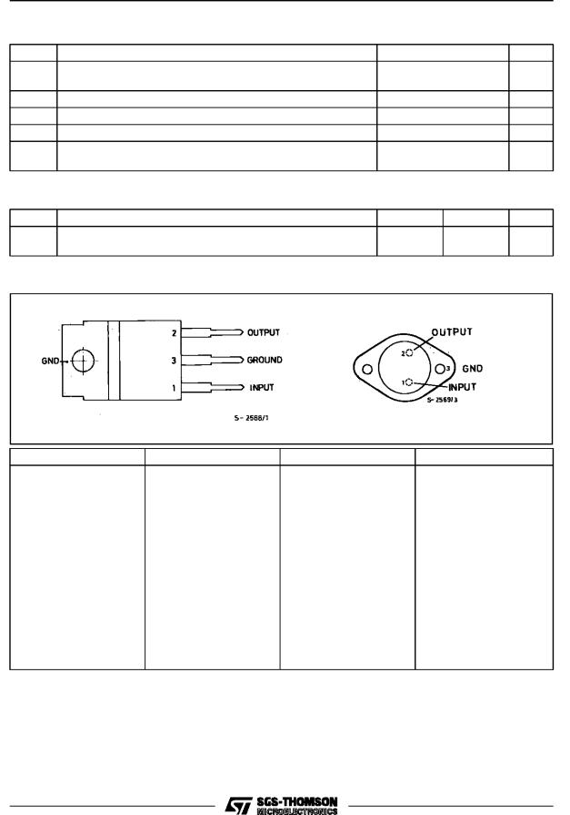
TO-3
TO-220
BLOCK DIAGRAM
January 1993 |
1/21 |
L78S00 SERIES
ABSOLUTE MAXIMUM RATINGS
Symbol
Vi
Io
Pt o t
T s t g
To p
Parameter |
Value |
Unit |
DC Input Voltage (for Vo = 5 to 18V) |
35 |
V |
(for Vo = 24V) |
40 |
V |
Output Current |
Internally limited |
|
Power Dissipation |
Internally limited |
|
Storage Temperature |
± 65 to + 150 |
°C |
Operating Junction Temperature (for L78S00 ) |
± 55 to + 150 |
°C |
(for L78S00C ) |
0 to + 150 |
°C |
THERMAL DATA
|
|
|
TO-220 |
TO-3 |
|
Rt h j- cas e |
Thermal Resistance Junction-case |
Max |
3 |
4 |
°C/W |
Rt h j -amb |
Thermal Resistance Junction-ambient |
Max |
50 |
35 |
°C/W |
CONNECTION DIAGRAMS AND ORDERING NUMBERS (top views)
Type |
T O- 22 0 |
T O - 3 |
Output Voltage |
L78S05 |
|
L78S05T |
5 V |
L78S05C |
L78S05CV |
L78S05CT |
5 V |
L78S75 |
|
L78S75T |
7.5V |
L78S75C |
L78S75CV |
L78S75CT |
7.5V |
L78S09 |
|
L78S09T |
9 V |
L78S09C |
L78S09CV |
L78S09CT |
9 V |
L78S10 |
|
L78S10T |
10V |
L78S10C |
L78S10CV |
L78S10CT |
10V |
L78S12 |
|
L78S12T |
12V |
L78S12C |
L78S12CV |
L78S12CT |
12V |
L78S15 |
|
L78S15T |
15V |
L78S15C |
L78S15CV |
L78S15CT |
15V |
L78S18 |
|
L78S18T |
18V |
L78S18C |
L78S18CV |
L78S18CT |
18V |
L78S24 |
|
L78S24T |
24V |
L78S24C |
L78S24CV |
L78S24CT |
24V |
2/21
L78S00 SERIES
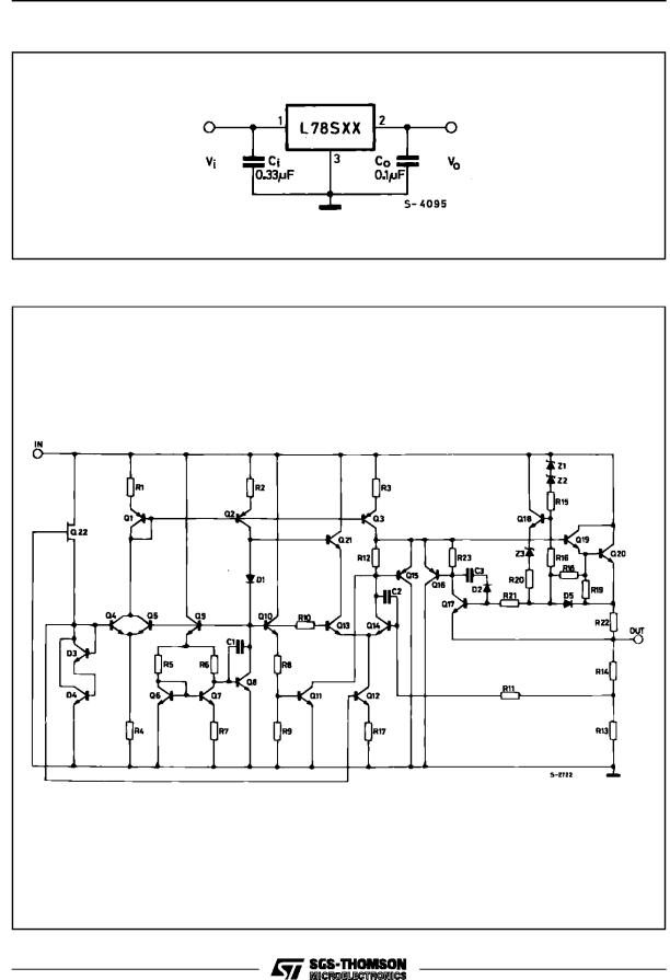
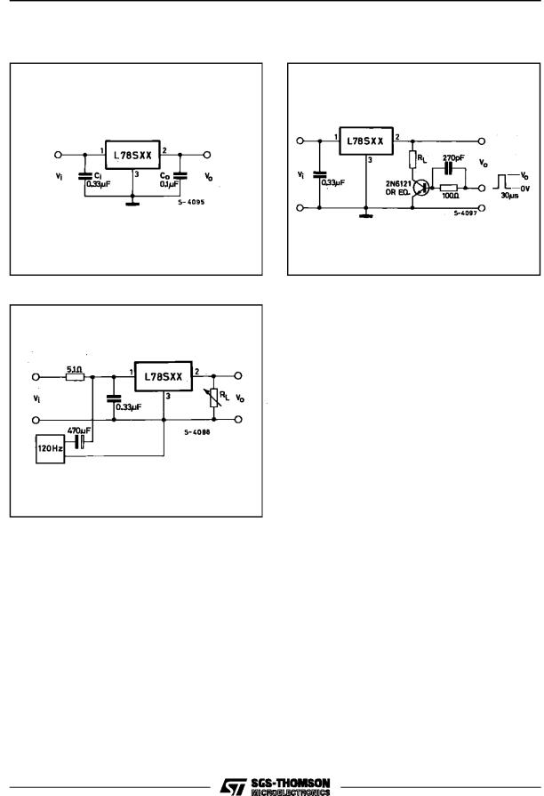
APPLICATION CIRCUIT
SCHEMATIC DIAGRAM
3/21
L78S00 SERIES
TEST CIRCUITS |
|
Figure 1 : DC Parameters. |
Figure 2 : Load Regulation. |
Figure 3 : Ripple Rejection.
4/21

L78S00 SERIES
ELECTRICAL CHARACTERISTICS FOR L78S05 (refer to the test circuits, Tj = 25 oC, Vi = 10V, Io = 500 mA unless otherwise specified)
Symbol |
Parameter |
Test Conditions |
Min. |
Typ. |
Max. |
Unit |
|
Vo |
Output Voltage |
|
|
4.8 |
5 |
5.2 |
V |
Vo |
Output Voltage |
Io = 1 A |
Vi = 7 V |
4.75 |
5 |
5.25 |
V |
Vo |
Line Regulation |
Vi = 7 to 25 V |
|
|
100 |
mV |
|
|
|
Vi = 8 to 25 V |
|
|
50 |
mV |
|
Vo |
Load Regulation |
Io = 20 mA |
to 2 A |
|
|
100 |
mV |
Id |
Quiescent Current |
|
|
|
|
8 |
mA |
Id |
Quiescent Current Change |
Io = 20 mA to 1A |
|
|
0.5 |
mA |
|
Id |
Quiescent Current Change |
Io = 20 mA |
Vi = 7 to 25 V |
|
|
1.3 |
mA |
Vo |
Output Voltage Drift |
Io = 5 mA |
Tj = -55 to 150 oC |
|
-1.1 |
|
mV/oC |
T |
|
|
|
|
|
|
|
eN |
Output Noise Voltage |
B = 10Hz to 100KHz |
|
40 |
|
μV |
|
SVR |
Supply Voltage Rejection |
f = 120 Hz |
|
60 |
|
|
dB |
Vi |
Operating Input Voltage |
Io ≤ 1.5 A |
|
8 |
|
|
V |
Ro |
Output Resistance |
f = 1KHz |
|
|
17 |
|
mΩ |
Isc |
Short Circuit Current |
Vi = 27 V |
|
|
500 |
|
mA |
Iscp |
Short Circuit Peack Current |
|
|
|
3 |
|
A |
ELECTRICAL CHARACTERISTICS FOR L78S75 (refer to the test circuits, Tj = 25 oC, Vi = 12.5V, Io = 500 mA unless otherwise specified)
Symbol |
Parameter |
Test Conditions |
Min. |
Typ. |
Max. |
Unit |
|
Vo |
Output Voltage |
|
|
7.15 |
7.5 |
7.9 |
V |
Vo |
Output Voltage |
Io = 1 A |
Vi = 9.5 V |
7.1 |
7.5 |
7.95 |
V |
Vo |
Line Regulation |
Vi = 9.5 to 25 V |
|
|
120 |
mV |
|
|
|
Vi = 10.5 to 20 V |
|
|
60 |
mV |
|
Vo |
Load Regulation |
Io = 20 mA |
to 2 A |
|
|
120 |
mV |
Id |
Quiescent Current |
|
|
|
|
8 |
mA |
Id |
Quiescent Current Change |
Io = 20 mA to 1A |
|
|
0.5 |
mA |
|
Id |
Quiescent Current Change |
Io = 20 mA |
Vi = 9.5 to 25 V |
|
|
1.3 |
mA |
Vo |
Output Voltage Drift |
Io = 5 mA |
Tj = -55 to 150 oC |
|
-0.8 |
|
mV/oC |
T |
|
|
|
|
|
|
|
eN |
Output Noise Voltage |
B = 10Hz to 100KHz |
|
52 |
|
μV |
|
SVR |
Supply Voltage Rejection |
f = 120 Hz |
|
54 |
|
|
dB |
Vi |
Operating Input Voltage |
Io ≤ 1.5 A |
|
10.5 |
|
|
V |
Ro |
Output Resistance |
f = 1KHz |
|
|
16 |
|
mΩ |
Isc |
Short Circuit Current |
Vi = 27 V |
|
|
500 |
|
mA |
Iscp |
Short Circuit Peack Current |
|
|
|
3 |
|
A |
5/21
L78S00 SERIES
ELECTRICAL CHARACTERISTICS FOR L78S09 (refer to the test circuits, Tj = 25 oC, Vi = 14V, Io = 500 mA unless otherwise specified)
Symbol |
Parameter |
Test Conditions |
Min. |
Typ. |
Max. |
Unit |
|
Vo |
Output Voltage |
|
|
8.65 |
9 |
9.35 |
V |
Vo |
Output Voltage |
Io = 1 A |
Vi = 11 V |
8.6 |
9 |
9.4 |
V |
Vo |
Line Regulation |
Vi = 11 to 25 V |
|
|
130 |
mV |
|
|
|
Vi = 11 to 20 V |
|
|
65 |
mV |
|
Vo |
Load Regulation |
Io = 20 mA |
to 2 A |
|
|
130 |
mV |
Id |
Quiescent Current |
|
|
|
|
8 |
mA |
Id |
Quiescent Current Change |
Io = 20 mA to 1A |
|
|
0.5 |
mA |
|
Id |
Quiescent Current Change |
Io = 20 mA |
Vi = 11 to 25 V |
|
|
1.3 |
mA |
Vo |
Output Voltage Drift |
Io = 5 mA |
Tj = -55 to 150 oC |
|
-1 |
|
mV/oC |
T |
|
|
|
|
|
|
|
eN |
Output Noise Voltage |
B = 10Hz to 100KHz |
|
60 |
|
μV |
|
SVR |
Supply Voltage Rejection |
f = 120 Hz |
|
53 |
|
|
dB |
Vi |
Operating Input Voltage |
Io ≤ 1.5 A |
|
12 |
|
|
V |
Ro |
Output Resistance |
f = 1KHz |
|
|
17 |
|
mΩ |
Isc |
Short Circuit Current |
Vi = 27 V |
|
|
500 |
|
mA |
Iscp |
Short Circuit Peack Current |
|
|
|
3 |
|
A |
ELECTRICAL CHARACTERISTICS FOR L78S10 (refer to the test circuits, Tj = 25 oC, Vi = 15V, Io = 500 mA unless otherwise specified)
Symbol |
Parameter |
Test Conditions |
Min. |
Typ. |
Max. |
Unit |
|
Vo |
Output Voltage |
|
|
9.5 |
10 |
10.5 |
V |
Vo |
Output Voltage |
Io = 1 A |
Vi = 12.5 V |
9.4 |
10 |
10.6 |
V |
Vo |
Line Regulation |
Vi = 12.5 to 30 V |
|
|
200 |
mV |
|
|
|
Vi = 14 to 22 V |
|
|
100 |
mV |
|
Vo |
Load Regulation |
Io = 20 mA |
to 2 A |
|
|
150 |
mV |
Id |
Quiescent Current |
|
|
|
|
8 |
mA |
Id |
Quiescent Current Change |
Io = 20 mA to 1A |
|
|
0.5 |
mA |
|
Id |
Quiescent Current Change |
Io = 20 mA |
Vi = 12.5 to 30 V |
|
|
1 |
mA |
Vo |
Output Voltage Drift |
Io = 5 mA |
Tj = -55 to 150 oC |
|
-1 |
|
mV/oC |
T |
|
|
|
|
|
|
|
eN |
Output Noise Voltage |
B = 10Hz to 100KHz |
|
65 |
|
μV |
|
SVR |
Supply Voltage Rejection |
f = 120 Hz |
|
53 |
|
|
dB |
Vi |
Operating Input Voltage |
Io ≤ 1.5 A |
|
13 |
|
|
V |
Ro |
Output Resistance |
f = 1KHz |
|
|
17 |
|
mΩ |
Isc |
Short Circuit Current |
Vi = 27 V |
|
|
500 |
|
mA |
Iscp |
Short Circuit Peack Current |
|
|
|
3 |
|
A |
6/21

L78S00 SERIES
ELECTRICAL CHARACTERISTICS FOR L78S12 (refer to the test circuits, Tj = 25 oC, Vi = 19V, Io = 500 mA unless otherwise specified)
Symbol |
Parameter |
Test Conditions |
Min. |
Typ. |
Max. |
Unit |
|
Vo |
Output Voltage |
|
|
11.5 |
12 |
12.5 |
V |
Vo |
Output Voltage |
Io = 1 A |
Vi = 14.5 V |
11.4 |
12 |
12.6 |
V |
Vo |
Line Regulation |
Vi = 14.5 to 30 V |
|
|
240 |
mV |
|
|
|
Vi = 16 to 22 V |
|
|
120 |
mV |
|
Vo |
Load Regulation |
Io = 20 mA |
to 2 A |
|
|
160 |
mV |
Id |
Quiescent Current |
|
|
|
|
8 |
mA |
Id |
Quiescent Current Change |
Io = 20 mA to 1A |
|
|
0.5 |
mA |
|
Id |
Quiescent Current Change |
Io = 20 mA |
Vi = 14.5 to 30 V |
|
|
1 |
mA |
Vo |
Output Voltage Drift |
Io = 5 mA |
Tj = -55 to 150 oC |
|
-1 |
|
mV/oC |
T |
|
|
|
|
|
|
|
eN |
Output Noise Voltage |
B = 10Hz to 100KHz |
|
75 |
|
μV |
|
SVR |
Supply Voltage Rejection |
f = 120 Hz |
|
53 |
|
|
dB |
Vi |
Operating Input Voltage |
Io ≤ 1.5 A |
|
15 |
|
|
V |
Ro |
Output Resistance |
f = 1KHz |
|
|
18 |
|
mΩ |
Isc |
Short Circuit Current |
Vi = 27 V |
|
|
500 |
|
mA |
Iscp |
Short Circuit Peack Current |
|
|
|
3 |
|
A |
ELECTRICAL CHARACTERISTICS FOR L78S15 (refer to the test circuits, Tj = 25 oC, Vi = 23V, Io = 500 mA unless otherwise specified)
Symbol |
Parameter |
Test Conditions |
Min. |
Typ. |
Max. |
Unit |
|
Vo |
Output Voltage |
|
|
14.4 |
15 |
15.6 |
V |
Vo |
Output Voltage |
Io = 1 A |
Vi = 17.5 V |
14.25 |
15 |
15.75 |
V |
Vo |
Line Regulation |
Vi = 17.5 to 30 V |
|
|
300 |
mV |
|
|
|
Vi = 20 to 26 V |
|
|
150 |
mV |
|
Vo |
Load Regulation |
Io = 20 mA |
to 2 A |
|
|
180 |
mV |
Id |
Quiescent Current |
|
|
|
|
8 |
mA |
Id |
Quiescent Current Change |
Io = 20 mA to 1A |
|
|
0.5 |
mA |
|
Id |
Quiescent Current Change |
Io = 20 mA |
Vi = 17.5 to 30 V |
|
|
1 |
mA |
Vo |
Output Voltage Drift |
Io = 5 mA |
Tj = -55 to 150 oC |
|
-1 |
|
mV/oC |
T |
|
|
|
|
|
|
|
eN |
Output Noise Voltage |
B = 10Hz to 100KHz |
|
90 |
|
μV |
|
SVR |
Supply Voltage Rejection |
f = 120 Hz |
|
52 |
|
|
dB |
Vi |
Operating Input Voltage |
Io ≤ 1.5 A |
|
18 |
|
|
V |
Ro |
Output Resistance |
f = 1KHz |
|
|
19 |
|
mΩ |
Isc |
Short Circuit Current |
Vi = 27 V |
|
|
500 |
|
mA |
Iscp |
Short Circuit Peack Current |
|
|
|
3 |
|
A |
7/21
 Loading...