


SGS Thomson Microelectronics L4957AV3.3, L4957AV2.5, L4957AV1.8, L4957AV1.5, L4957AD2.5 Datasheet
...
|
L4957A |
UP TO 5A ULDO LINEAR REGULATOR
PRODUCT PREVIEW
1.5V, 1.8V, 2.5V AND 3.3V FIXED OUTPUT VOLTAGE
3V TO 14V INPUT VOLTAGE RANGE 200mΩ Rdson TYPICAL @ Tj = 125°C 0.6V max. DROP-OUT AT 2A EXCELLENT LOAD REGULATION
0.6mAQUIESCENT CURRENT AT ANY LOAD SHORT CIRCUIT PROTECTION
THERMAL SHUTDOWN
MULTIPOWER BCD TECHNOLOGY
3
|
1 |
Versawatt TO-220 |
D2PAK |
ORDERING NUMBERS:
APPLICATIONS
MOTHER BOARDS PROCESSOR I/O & SUPPLIES
LOW VOLTAGE MEMORY & CHIP SET SUPPLIES
GRAPHIC & SOUND CARDS LOW VOLTAGE LOGIC SUPPLIES POST REGULATOR FOR SMPS
DESCRIPTION
The L4957A devices are Ultra Low Drop Output linear regulators with an internal N-channel MOS of 200mΩ particulary suitable for low voltage/low dropout applications.
Operating with a input voltage from 3V to 14V they are capable to deliver up to 5A.
The devices are ideal for use as one of the sup-
TYPICAL APPLICATION
L4957AV1.5 |
L4957AD1.5 |
L4957AV1.8 |
L4957AD1.8 |
L4957AV2.5 |
L4957AD2.5 |
L4957AV3.3 |
L4957AD3.3 |
plies required by processor, for example they are the cost effective and efficient solution for conversion from 3.3V (rail bus) to 2.5V @ 2.5A or to 1.5V with high current rating.
Fast response transient minimise the output capacitor value. A minimum of 22μF assures the stability in all load conditions.
The on-chip trimming technique offers a tighter voltage reference tolerance (with ± 2% including line and load variation) beside to ensure a controlled short circuit current. Thermal shutdown provides protection against overload conditions that creates excessive junction temperature.
3V to 14V IN |
OUT |
VOUT |
1 |
3 |
|
|
L4957A |
|
C1 |
|
C2 |
2
GND
D00IN1107A
May 2000 |
1/7 |
This is preliminary information on a new product now in development. Details are subject to change without notice.
L4957A
ABSOLUTE MAXIMUM RATINGS
Symbol |
Parameter |
Value |
Unit |
VIN |
Supply Input Voltage |
16 |
V |
Ti |
Junction Temperature |
-40 to +150 |
°C |
Tstg |
Storage Temperature |
-40 to +150 |
°C |
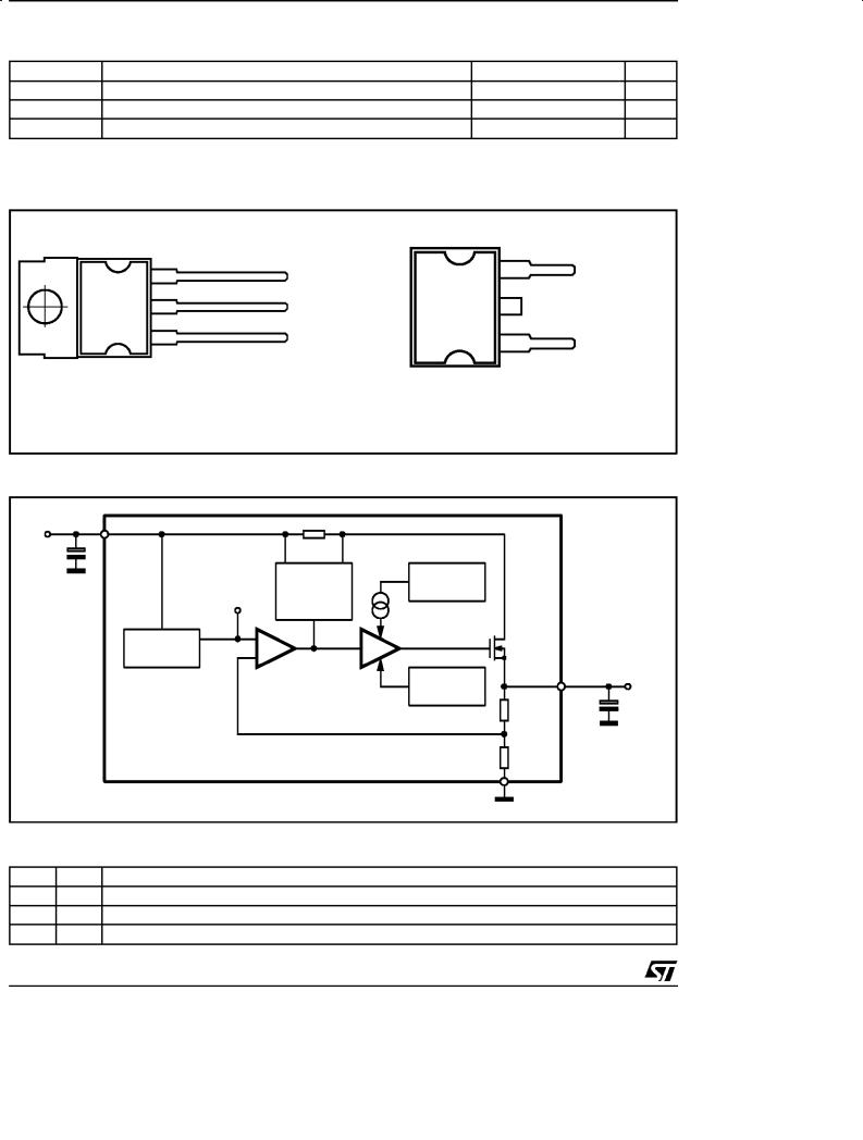
PINS CONNECTION
3 |
OUT |
3 |
OUT |
|
|
||
2 |
GND |
2 |
GND |
1 |
IN |
1 |
IN |
|
|
||
|
D98IN838B |
|
|
|
|
|
D98IN933A |
Versawatt (TO220) |
|
|
D2PAK |
BLOCK DIAGRAM
IN
VIN |
1 |
|
|
|
|
10μF |
|
|
|
|
|
|
|
|
|
|
|
|
|
CURRENT |
CHARGE |
|
|
|
VREF |
PUMP |
|
|
|
|
LIMIT |
|
|
|
|
|
PRE |
+ |
BUFFER |
POWER |
|
|
E/A |
|
DMOS |
|
|
|
REGULATOR |
|
|
||
|
- |
|
|
||
|
|
200mΩ |
|
||
|
|
|
|
|
|
|
|
|
THERMAL |
|
OUT |
|
|
|
|
VOUT |
|
|
|
|
SHUTDOWN |
3 |
|
|
|
|
|
RX |
22μF |
|
|
|
|
RY |
|
|
|
|
2 |
|
|
|
|
|
GND |
|
D00IN1108A |
|
|
|
|
|
PIN FUNCTIONS
Pin N° |
Name |
Function |
1 |
IN |
Unregulated input voltage; this pin must be bypassed with a capacitor larger than 10μF. |
2 |
GND |
To connect to Ground to get 1.5V, 1.8V, 2.5V or 3.3V output. |
3 |
OUT |
Regulated output voltage. A minimum bypass capacitor of 22μF is required to insure stability. |
2/7

|
|
|
|
|
|
|
|
L4957A |
THERMAL DATA |
|
|
|
|
|
|
|
|
Symbol |
|
Parameter |
|
|
TO220 |
|
D2PAK |
Unit |
Rth j-case |
Thermal Resistance Junction-case |
|
Max. |
2.5 |
|
3 |
°C/W |
|
Rth j-amb |
Thermal Resistance Junction-ambient |
|
Max. |
50 |
|
60 |
°C/W |
|
|
Thermal Shutdown |
|
|
Typ. |
|
150 |
|
°C |
|
Thermal Hysteresis |
|
|
Typ. |
|
20 |
|
°C |
ELECTRICAL CHARACTERISTICS (Tj = 25°C, VIN = 5V, unless otherwise specified). |
|
|
||||||
•= Specifications referred to TJ from 0°C to +125°C. |
|
|
|
|
|
|||
Symbol |
Parameter |
Test Condition |
|
Min. |
Typ. |
Max. |
Unit |
|
VIN |
Operating Supply Voltage |
|
|
|
3 |
|
14 |
V |
VO |
Output Voltage |
3.15V < VIN < 5.25V; IO = 0.1A |
• |
1.485 |
1.5 |
1.515 |
V |
|
|
|
VIN = 3.3V ±5%; 0.1A < IO < 5A |
1.47 |
1.5 |
1.53 |
V |
||
|
|
VIN = 3.3V ±5% |
IO = 0.1A |
|
1.782 |
1.8 |
1.818 |
V |
|
|
VIN = 5V ±5% |
|
• |
|
|
|
|
|
|
VIN = 3.3V ±5% |
(0.1A < IO < 45A) |
1.764 |
1.8 |
1.836 |
V |
|
|
|
VIN = 5V ±5% |
0.1A < IO < 5A |
|
|
|
|
|
|
|
VIN = 3.3V ±5% |
IO = 0.1A |
|
2.475 |
2.5 |
2.525 |
V |
|
|
VIN = 5V ±5% |
|
• |
|
|
|
|
|
|
VIN = 3.3V ±5% (0.1A < IO < 2.2A) |
2.45 |
2.5 |
2.55 |
V |
||
|
|
VIN = 5V ±5% |
0.1A < IO < 5A |
|
|
|
|
|
|
|
VIN = 5V ±5% |
IO = 0.1A |
• |
3.267 |
3.3 |
3.333 |
V |
|
|
VIN = 5V ±5% |
0.1A < IO < 5A |
3.234 |
3.3 |
3.366 |
V |
|
RDSON |
Drain-Source ON |
|
|
• |
|
|
300 |
mΩ |
|
Resistance |
|
|
• |
|
|
|
|
IO |
Current Limiting |
|
|
5.1 |
6.3 |
7.5 |
A |
|
IQ |
Quiescent Current |
3V < VIN < 14V |
|
• |
|
0.6 |
2 |
mA |
|
Ripple Rejection |
f = 120Hz, IO = 1A |
|
60 |
75 |
|
dB |
|
|
|
VIN = 5V VIN = 2VPP |
|
|
|
|
|
|
Figure 1: Line Regulation vs. Junction Temperature
[mV] |
5 |
|
4.5 |
|
|
Deviation |
|
|
3.5 |
3V < Vin < 6.5V |
|
|
4 |
Iout = 10mA |
Voltage |
|
|
3 |
|
|
|
|
|
Output |
2.5 |
|
2 |
|
|
|
|
|
|
1.5 |
|
|
1 |
|
0.5
0 -40 -20 0 20 40 60 80 100 120 140 160
Tj [°C]
Figure 2: Load Regulation
[mV] |
5 |
|
|
4 |
|
||
Deviation |
Vin = 5V |
||
|
|||
|
3 |
Tj = 25 °C |
|
|
(Pulsed technique has been used) |
||
|
|
||
Voltage |
2 |
Vout = 1.5V |
|
1 |
|
||
Output |
|
||
0 |
|
||
|
|
-1 -2 -3 -4
-5
0 |
1 |
2 |
3 |
4 |
5 |
|
|
|
Iout [A] |
|
|
3/7
 Loading...