


HCC/HCF4511B
BCD-TO-SEVEN SEGMENT LATCH/DECODER/DRIVER
.HIGH-OUTPUT-SOURCING CAPABILITY (up
.to 25 mA)
.INPUT LATCHES FOR BCD CODE STORAGE
.LAMP TEST AND BLANKING CAPABILITY 7-SEGMENT OUTPUTS BLANKED FOR BCD
.INPUT CODES > 1001
QUIESCENT CURRENT SPECIFIED TO 20V
.FOR HCC DEVICE
STANDARDIZED SYMMETRICAL OUTPUT
.CHARACTERISTICS
.5V, 10V, AND 15V PARAMETRIC RATINGS INPUT CURRENT OF 100mA AT 18V AND 25°C
.FOR HCC DEVICE
.100% TESTED FOR QUIESCENT CURRENT MEETS ALL REQUIREMENTS OF JEDECTENTATIVE STANDARD N°13A, ºSTANDARD SPECIFICATIONS FOR DESCRIPTION OF ºBº SERIES CMOS DEVICESº
EY |
F |
(Plastic Package) |
(Ceramic Frit Seal Package) |
M1 |
C1 |
(Micro Package) |
(Plastic Chip Carrier) |
ORDER CODES :
HCC4511BF HCF4511BM1
HCF4511BEY HCF4511BC1
PIN CONNECTIONS
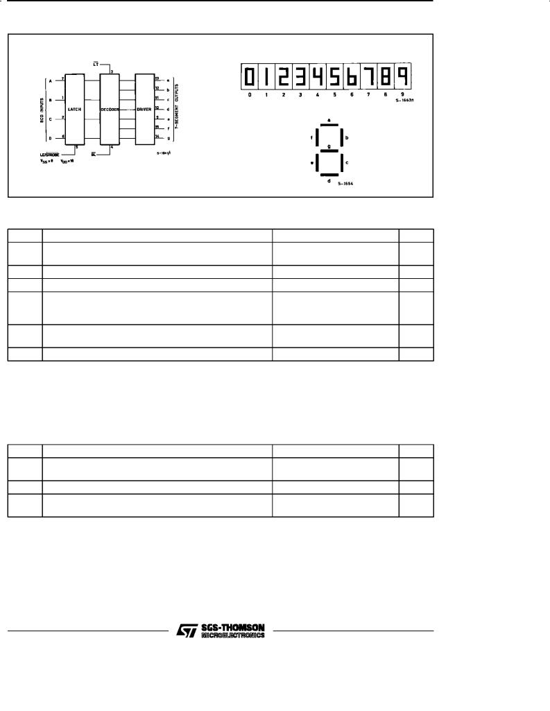
DESCRIPTION
The HCC 4511B (extended temperature range) and the HCF 4511B (intermediate temperature range) are monolithic integrated circuits available in 16-le- ad dual in-line plastic or ceramic package and plastic micro package.
The HCC/HCF 4511B types are BCD-to-7-segment latch decoder drivers constructed with COS/MOS logic and n-p-n bipolar transistor output devices on a single monolithic structure. These devices combine the low quiescent power dissipation and high noise immunity features of COS/MOS with n-p-n bipolar output transistors capable of sourcing up to 25 mA. This capability allows the HCC/HCF 4511B types to drive LED's and other displays directly.
Lamp Test (LT), Blanking (BL), and Latch Enable or Strobe inputs are provided to test the display, shut off or intensity-modulate it, and store or strobe a BCD code, respectively. Several different signal may be multiplexed and displayed when external multiplexing circuitry is used.
November 1996 |
1/16 |
HCC/HFC4511B
FUNCTIONAL DIAGRAM
ABSOLUTE MAXIMUM RATINGS
Symbol
V DD*
Vi
II
Pt o t
T o p
Ts t g
Parameter |
Value |
Unit |
Supply Voltage : HC C Types |
± 0.5 to + 20 |
V |
H C F Types |
± 0.5 to + 18 |
V |
Input Voltage |
± 0.5 to VDD + 0.5 |
V |
DC Input Current (any one input) |
± 10 |
mA |
Total Power Dissipation (per package) |
200 |
mW |
Dissipation per Output Transistor |
|
|
for To p = Full Package-temperature Range |
100 |
mW |
Operating Temperature : HCC Types |
± 55 to + 125 |
°C |
H CF Types |
± 40 to + 85 |
°C |
Storage Temperature |
± 65 to + 150 |
°C |
Stresses above those listed under ºAbsolute Maximum Ratingsº may cause permanent damage to the device. This is a stress rating only and functionnal operation of the device at these or any other conditions above those indicated in the operational sections of this specification is not implied. Exposure to absolute maximum rating conditions for external periods may affect device reliability.
* All voltage values are referred to VSS pin voltage.
RECOMMENDED OPERATING CONDITIONS
Symbol |
Parameter |
Value |
Unit |
VDD |
Supply Voltage : H CC Types |
3 to 18 |
V |
|
H C F Types |
3 to 15 |
V |
VI |
Input Voltage |
0 to VDD |
V |
T o p |
Operating Temperature : HCC Types |
± 55 to + 125 |
°C |
|
H CF Types |
± 40 to + 85 |
°C |
2/16
HCC/HCF4511B
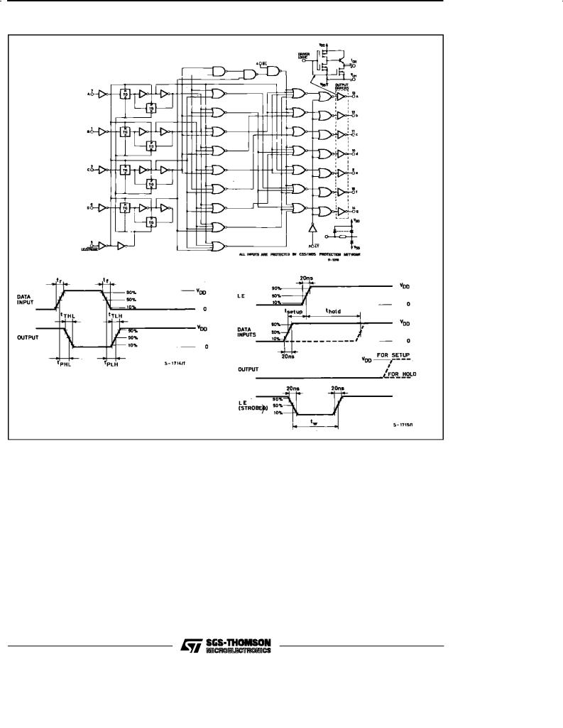
LOGIC DIAGRAMS
3/16
HCC/HFC4511B
TRUTH TABLE
LE |
BI |
L T |
D |
C |
B |
A |
a |
b |
c |
d |
e |
f |
g |
Display |
X |
X |
0 |
X |
X |
X |
X |
1 |
1 |
1 |
1 |
1 |
1 |
1 |
8 |
|
|
|
|
|
|
|
|
|
||||||
X |
0 |
1 |
X |
X |
X |
X |
0 |
0 |
0 |
0 |
0 |
0 |
0 |
Blank |
0 |
1 |
1 |
0 |
0 |
0 |
0 |
1 |
1 |
1 |
1 |
1 |
1 |
0 |
0 |
|
|
|
|
|
|
|
|
|
||||||
0 |
1 |
1 |
0 |
0 |
0 |
1 |
0 |
1 |
1 |
0 |
0 |
0 |
0 |
1 |
|
|
|
|
|
|
|
|
|
||||||
0 |
1 |
1 |
0 |
0 |
1 |
0 |
1 |
1 |
0 |
1 |
1 |
0 |
1 |
2 |
|
|
|
|
|
|
|
|
|
||||||
0 |
1 |
1 |
0 |
0 |
1 |
1 |
1 |
1 |
1 |
1 |
0 |
0 |
1 |
3 |
|
|
|
|
|
|
|
|
|
||||||
0 |
1 |
1 |
0 |
1 |
0 |
0 |
0 |
1 |
1 |
0 |
0 |
1 |
1 |
4 |
|
|
|
|
|
|
|
|
|
||||||
0 |
1 |
1 |
0 |
1 |
0 |
1 |
1 |
0 |
1 |
1 |
0 |
1 |
1 |
5 |
|
|
|
|
|
|
|
|
|
||||||
0 |
1 |
1 |
0 |
1 |
1 |
0 |
0 |
0 |
1 |
1 |
1 |
1 |
1 |
6 |
|
|
|
|
|
|
|
|
|
||||||
0 |
1 |
1 |
0 |
1 |
1 |
1 |
1 |
1 |
1 |
0 |
0 |
0 |
0 |
7 |
|
|
|
|
|
|
|
|
|
||||||
0 |
1 |
1 |
1 |
0 |
0 |
0 |
1 |
1 |
1 |
1 |
1 |
1 |
1 |
8 |
|
|
|
|
|
|
|
|
|
||||||
0 |
1 |
1 |
1 |
0 |
0 |
1 |
1 |
1 |
1 |
0 |
0 |
1 |
1 |
9 |
|
|
|
|
|
|
|
|
|
||||||
0 |
1 |
1 |
1 |
0 |
1 |
0 |
0 |
0 |
0 |
0 |
0 |
0 |
0 |
Blank |
0 |
1 |
1 |
1 |
0 |
1 |
1 |
0 |
0 |
0 |
0 |
0 |
0 |
0 |
Blank |
0 |
1 |
1 |
1 |
1 |
0 |
0 |
0 |
0 |
0 |
0 |
0 |
0 |
0 |
Blank |
0 |
1 |
1 |
1 |
1 |
0 |
1 |
0 |
0 |
0 |
0 |
0 |
0 |
0 |
Blank |
0 |
1 |
1 |
1 |
1 |
1 |
0 |
0 |
0 |
0 |
0 |
0 |
0 |
0 |
Blank |
0 |
1 |
1 |
1 |
1 |
1 |
1 |
0 |
0 |
0 |
0 |
0 |
0 |
0 |
Blank |
1 |
1 |
1 |
X |
X |
X |
X |
|
|
|
* |
|
|
|
* |
4/16

HCC/HCF4511B
STATIC ELECTRICAL CHARACTERISTICS (over recommended operating conditions)
Symbol
IL
VOH
VOL
VIH
VIL
VOH
Parameter
Quiescent
Current
HCC
Types
HCF
Types
Output High
Voltage
Output Low
Voltage
Input High
Voltage
Input Low
Voltage
Output HCC
Drive Types
Voltage
Test Conditions |
|
|
|
Value |
|
|
|
||
V I |
V O |
|I O | V D D |
T L o w* |
|
° |
|
T Hi g h * |
Unit |
|
|
25 C |
|
|
||||||
(V) |
(V) |
(μA) (V) |
Min. Max. Min. Typ. Max. Min. Max. |
|
|||||
|
|
|
|
|
|||||
0/ 5 |
|
|
5 |
5 |
|
0.04 |
5 |
150 |
|
0/10 |
|
|
10 |
10 |
|
0.04 |
10 |
300 |
|
0/15 |
|
|
15 |
20 |
|
0.04 |
20 |
600 |
|
0/20 |
|
|
20 |
100 |
|
0.08 |
100 |
3000 |
μA |
0/ 5 |
|
|
5 |
20 |
|
0.04 |
20 |
150 |
|
0/10 |
|
|
10 |
40 |
|
0.04 |
40 |
300 |
|
0/15 |
|
|
15 |
80 |
|
0.04 |
80 |
600 |
|
0/ 5 |
|
|
5 |
4 |
4.1 |
4.55 |
|
4.2 |
|
0/10 |
|
|
10 |
9 |
9.1 |
9.55 |
|
9.2 |
V |
0/15 |
|
|
15 |
14 |
14.1 |
14.55 |
|
14.2 |
|
5/0 |
|
|
5 |
0.05 |
|
|
0.05 |
0.05 |
|
10/0 |
|
|
10 |
0.05 |
|
|
0.05 |
0.05 |
V |
15/0 |
|
|
15 |
0.05 |
|
|
0.05 |
0.05 |
|
|
0.5/3.8 |
|
5 |
3.5 |
3.5 |
|
|
3.5 |
|
|
1/8.8 |
|
10 |
7 |
7 |
|
|
7 |
V |
|
1.5/13.8 |
|
15 |
11 |
11 |
|
|
11 |
|
|
3.8/0.5 |
|
5 |
1.5 |
|
|
1.5 |
1.5 |
|
|
8.8/1 |
|
10 |
3 |
|
|
3 |
3 |
V |
|
13.8/1.5 |
|
15 |
4 |
|
|
4 |
4 |
|
|
|
0 |
|
4.1 |
4.10 |
4.55 |
|
4.20 |
|
|
|
5 |
|
|
|
4.25 |
|
|
|
|
|
10 |
5 |
3.80 |
3.90 |
4.10 |
|
3.90 |
V |
|
|
15 |
|
|
3.95 |
|
|
||
|
|
|
|
|
|
|
|
||
|
|
20 |
|
3.55 |
3.40 |
3.75 |
|
|
|
|
|
25 |
|
3.40 |
3.10 |
3.55 |
|
|
|
|
|
0 |
|
9 |
9.10 |
9.55 |
|
9.20 |
|
|
|
5 |
|
|
|
9.25 |
|
|
|
|
|
10 |
10 |
8.85 |
9 |
9.15 |
|
|
V |
|
|
15 |
|
|
9.05 |
|
|
||
|
|
|
|
|
|
|
|
||
|
|
20 |
|
8.70 |
8.60 |
8.90 |
|
8.40 |
|
|
|
25 |
|
8.60 |
8.30 |
8.75 |
|
|
|
|
|
0 |
|
14 |
14.10 |
14.55 |
|
14.20 |
|
|
|
5 |
|
|
|
14.30 |
|
|
|
|
|
10 |
15 |
13.90 |
14 |
14.20 |
|
14 |
V |
|
|
15 |
|
|
14.10 |
|
|
||
|
|
|
|
|
|
|
|
||
|
|
20 |
|
13.75 |
13.70 |
13.95 |
|
13.50 |
|
|
|
25 |
|
13.65 |
13.50 |
13.80 |
|
13.10 |
|
*TLow= ± 55°C for HCC device : ± 40°C for HCF device.
*THigh= + 125°C for HCC device : + 85°C for HCF device.
The Noise Margin for both º1º and º0º level is : 1V min. with V DD = 5V, 2V min. with VDD = 10V, 2.5 V min. with VDD = 15V.
5/16
 Loading...