


INTEGRATED CIRCUITS
80C552/83C552
Single-chip 8-bit microcontroller
Product specification |
1996 Aug 06 |
IC20 Data Handbook
m n r

Philips Semiconductors |
Product specification |
|
|
|
|
Single-chip 8-bit microcontroller |
80C552/83C552 |
|
|
|
|
Single-chip 8-bit microcontroller with 10-bit A/D, capture/compare timer, high-speed outputs, PWM
DESCRIPTION
The 80C552/83C552 (hereafter generically referred to as 8XC552) Single-Chip 8-Bit Microcontroller is manufactured in an advanced CMOS process and is a derivative of the 80C51 microcontroller family. The 8XC552 has the same instruction set as the 80C51. Three versions of the derivative exist:
•83C552Ð8k bytes mask programmable ROM
•80C552ÐROMless version of the 83C552
•87C552Ð8k bytes EPROM (described in a separate chapter)
The 8XC552 contains a non-volatile 8k × 8 read-only program memory (83C552), a volatile 256 × 8 read/write data memory, five 8-bit I/O ports, one 8-bit input port, two 16-bit timer/event counters (identical to the timers of the 80C51), an additional 16-bit timer coupled to capture and compare latches, a 15-source, two-priority-level, nested interrupt structure, an 8-input ADC, a dual DAC pulse width modulated interface, two serial interfaces (UART and I2C-bus), a ªwatchdogº timer and on-chip oscillator and timing circuits. For systems that require extra capability, the 8XC552 can be expanded using standard TTL compatible memories and logic.
In addition, the 8XC552 has two software selectable modes of power reductionÐidle mode and power-down mode. The idle mode freezes the CPU while allowing the RAM, timers, serial ports, and interrupt system to continue functioning. The power-down mode saves the RAM contents but freezes the oscillator, causing all other chip functions to be inoperative.
The device also functions as an arithmetic processor having facilities for both binary and BCD arithmetic plus bit-handling capabilities. The instruction set consists of over 100 instructions: 49 one-byte, 45 two-byte, and 17 three-byte. With a 16MHz (24MHz) crystal, 58% of the instructions are executed in 0.75ms (0.5ms) and 40% in 1.5ms (1ms). Multiply and divide instructions require 3ms (2ms).
FEATURES
•80C51 central processing unit
•8k × 8 ROM expandable externally to 64k bytes
•An additional 16-bit timer/counter coupled to four capture registers and three compare registers
•Two standard 16-bit timer/counters
•256 × 8 RAM, expandable externally to 64k bytes
•Capable of producing eight synchronized, timed outputs
•A 10-bit ADC with eight multiplexed analog inputs
•Two 8-bit resolution, pulse width modulation outputs
•Five 8-bit I/O ports plus one 8-bit input port shared with analog inputs
•I2C-bus serial I/O port with byte oriented master and slave functions
•Full-duplex UART compatible with the standard 80C51
•On-chip watchdog timer
•Three speed ranges:
±1.2 to 16MHz
±1.2 to 24MHz (ROM, ROMless only)
±1.2 to 30MHz (ROM, ROMless only)
•Three operating ambient temperature ranges:
±PCB83C552±5: 0°C to +70°C
±PCF83C552±5: ±40°C to +85°C (XTAL frequency max. 24 MHz)
±PCA83C552±5: ±40°C to +125°C (XTAL frequency max. 16 MHz)
PIN CONFIGURATIONS
|
9 |
1 |
61 |
|
|
10 |
|
|
60 |
|
CERAMIC |
|
|
|
|
|
AND |
|
|
|
PLASTIC |
|
|
|
|
LEADED CHIP |
|
||
|
CARRIER |
|
|
|
|
26 |
|
|
44 |
|
27 |
|
43 |
|
Pin |
Function |
|
Pin |
Function |
1 |
P5.0/ADC0 |
|
35 |
XTAL1 |
2 |
VDD |
|
36 |
VSS |
3 |
STADC |
|
37 |
VSS |
4 |
PWM0 |
|
38 |
NC* |
5 |
PWM1 |
|
39 |
P2.0/A08 |
6 |
EW |
|
40 |
P2.1/A09 |
7 |
P4.0/CMSR0 |
|
41 |
P2.2/A10 |
8 |
P4.1/CMSR1 |
|
42 |
P2.3/A11 |
9 |
P4.2/CMSR2 |
|
43 |
P2.4/A12 |
10 |
P4.3/CMSR3 |
|
44 |
P2.5/A13 |
11 |
P4.4/CMSR4 |
|
45 |
P2.6/A14 |
12 |
P4.5/CMSR5 |
|
46 |
P2.7/A15 |
13 |
P4.6/CMT0 |
|
47 |
PSEN |
14 |
P4.7/CMT1 |
|
48 |
ALE |
15 |
RST |
|
49 |
EA |
16 |
P1.0/CT0I |
|
50 |
P0.7/AD7 |
17 |
P1.1/CT1I |
|
51 |
P0.6/AD6 |
18 |
P1.2/CT2I |
|
52 |
P0.5/AD5 |
19 |
P1.3/CT3I |
|
53 |
P0.4/AD4 |
20 |
P1.4/T2 |
|
54 |
P0.3/AD3 |
21 |
P1.5/RT2 |
|
55 |
P0.2/AD2 |
22 |
P1.6/SCL |
|
56 |
P0.1/AD1 |
23 |
P1.7/SDA |
|
57 |
P0.0/AD0 |
24 |
P3.0/RxD |
|
58 |
AVref± |
25 |
P3.1/TxD |
|
59 |
AVref+ |
26 |
P3.2/INT0 |
|
60 |
AVSS |
27 |
P3.3/INT1 |
|
61 |
AVDD |
28 |
P3.4/T0 |
|
62 |
P5.7/ADC7 |
29 |
P3.5/T1 |
|
63 |
P5.6/ADC6 |
30 |
P3.6/WR |
|
64 |
P5.5/ADC5 |
31 |
P3.7/RD |
|
65 |
P5.4/ADC4 |
32 |
NC* |
|
66 |
P5.3/ADC3 |
33 |
NC* |
|
67 |
P5.2/ADC2 |
34 |
XTAL2 |
|
68 |
P5.1/ADC1 |
*DO NOT CONNECT
80 |
65 |
1 |
64 |
|
PLASTIC |
|
QUAD FLAT |
|
PACK |
24 |
41 |
25 40
1996 Aug 06 |
2 |
Philips Semiconductors
Single-chip 8-bit microcontroller
PLASTIC QUAD FLAT PACK PIN FUNCTIONS
|
|
|
|
|
|
80 |
|
65 |
|
|
|
|
|
|
|
|
|
|
|
|
|
|
|
|
|
|
|
|
|
|
|
|
|
|
|
|
|
|
|
|
|
|
|
|
|
|
|
|
|
|
|
|
1 |
|
|
|
|
|
|
|
64 |
|
|
|
|
|
|
|
|
|
|
|
|
|
PQFP |
|
|
|
|
|
|
|
|
|
|
|
|
|
|
|
|
|
|
|
|
|
|
|
|
||
|
|
|
|
|
|
|
|
|
|
|
|
|
|
|
|
|
|
|
24 |
|
|
|
|
|
|
|
41 |
|
|
|
|
|
|
|
|
|
|
|
|
|
|
|
|
|
|
|
|
|
|
|
|
|
|
|
|
|
|
|
|
|
|
|
|
|
|
|
|
|
|
|
|
|
25 |
|
40 |
|
|
|
|
|
|
|
||
|
|
|
|
|
|
|
|
|
|
|
|
|
|
|
|
|
Pin |
Function |
Pin |
|
Function |
||||||||||||
1 |
P4.1/CMSR1 |
41 |
|
P2.3/A11 |
||||||||||||
2 |
P4.2/CMSR2 |
42 |
|
P2.4/A12 |
||||||||||||
3 |
NC* |
43 |
|
NC* |
||||||||||||
4 |
P4.3/CMSR3 |
44 |
|
NC* |
||||||||||||
5 |
P4.4/CMSR4 |
45 |
|
P2.5/A13 |
||||||||||||
6 |
P4.5/CMSR5 |
46 |
|
P2.6/A14 |
||||||||||||
7 |
P4.6/CMT0 |
47 |
|
P2.7/A15 |
||||||||||||
8 |
P4.7/CMT1 |
48 |
|
|
|
|
|
|
||||||||
|
PSEN |
|||||||||||||||
9 |
RST |
49 |
|
ALE |
||||||||||||
10 |
P1.0/CT0I |
50 |
|
|
|
|
|
|||||||||
|
EA |
|||||||||||||||
11 |
P1.1/CT1I |
51 |
|
P0.7/AD7 |
||||||||||||
12 |
P1.2/CT2I |
52 |
|
P0.6/AD6 |
||||||||||||
13 |
P1.3/CT3I |
53 |
|
P0.5/AD5 |
||||||||||||
14 |
P1.4/T2 |
54 |
|
P0.4/AD4 |
||||||||||||
15 |
P1.5/RT2 |
55 |
|
P0.3/AD3 |
||||||||||||
16 |
P1.6/SCL |
56 |
|
P0.2/AD2 |
||||||||||||
17 |
P1.7/SDA |
57 |
|
P0.1/AD1 |
||||||||||||
18 |
P3.0/RxD |
58 |
|
P0.0/AD0 |
||||||||||||
19 |
P3.1/TxD |
59 |
|
AVref± |
||||||||||||
20 |
|
|
|
|
|
60 |
|
AVref+ |
||||||||
P3.2/INT0 |
|
|||||||||||||||
21 |
NC* |
61 |
|
AVSS |
||||||||||||
22 |
NC* |
62 |
|
NC* |
||||||||||||
23 |
|
|
|
|
|
63 |
|
AVDD |
||||||||
P3.3/INT1 |
|
|||||||||||||||
24 |
P3.4/T0 |
64 |
|
P5.7/ADC7 |
||||||||||||
25 |
P3.5/T1 |
65 |
|
P5.6/ADC6 |
||||||||||||
26 |
|
|
|
|
66 |
|
P5.5/ADC5 |
|||||||||
P3.6/WR |
|
|||||||||||||||
27 |
|
|
|
67 |
|
P5.4/ADC4 |
||||||||||
P3.7/RD |
|
|||||||||||||||
28 |
NC* |
68 |
|
P5.3/ADC3 |
||||||||||||
29 |
NC* |
69 |
|
P5.2/ADC2 |
||||||||||||
30 |
NC* |
70 |
|
P5.1/ADC1 |
||||||||||||
31 |
XTAL2 |
71 |
|
P5.0/ADC0 |
||||||||||||
32 |
XTAL1 |
72 |
|
VDD |
||||||||||||
33 |
IC |
73 |
|
IC |
||||||||||||
34 |
VSS |
74 |
|
STADC |
||||||||||||
35 |
VSS |
75 |
|
|
|
|
||||||||||
|
PWM0 |
|||||||||||||||
36 |
VSS |
76 |
|
|
|
|
||||||||||
|
PWM1 |
|||||||||||||||
37 |
NC* |
77 |
|
|
|
|||||||||||
|
EW |
|||||||||||||||
38 |
P2.0/A08 |
78 |
|
NC* |
||||||||||||
39 |
P2.1/A09 |
79 |
|
NC* |
||||||||||||
40 |
P2.2/A10 |
80 |
|
P4.0/CMSR0 |
||||||||||||
* DO NOT CONNECT
IC = internally connected (do not use)
LOGIC SYMBOL
VSS
VDD
XTAL1
XTAL2
EA
ALE
PSEN
AVSS
AVDD
AVref+
AVref±
STADC
PWM0
PWM1
ADC0-7
5PORT
CMSR0-5
4PORT


CMT0 
CMT1 
RST
EW
Product specification
80C552/83C552
0 |
LOW ORDER |
|
PORT |
||
ADDRESS AND |
||
|
||
|
DATA BUS |
|
|
CT0I |
|
|
CT1I |
|
1 |
CT2I |
|
CT3I |
||
PORT |
||
RT2 |
||
|
T2 |
|
|
SCL |
|
|
SDA |
|
2 |
HIGH ORDER |
|
PORT |
||
ADDRESS AND |
||
|
DATA BUS |
RxD/DATA
 TxD/CLOCK
3 |
INT0 |
PORT |
INT1 |
|
|
|
T0 |
|
T1 |
|
WR |
|
RD |
1996 Aug 06 |
3 |

Philips Semiconductors |
|
|
|
|
Product specification |
||
|
|
|
|
|
|
|
|
Single-chip 8-bit microcontroller |
|
|
80C552/83C552 |
||||
|
|
|
|
|
|
|
|
ORDERING INFORMATION |
|
|
|
|
|
||
|
|
|
|
|
|
|
|
PHILIPS |
NORTH AMERICA PHILIPS |
|
|
|
|||
PART ORDER NUMBER |
|
|
|
||||
PART ORDER NUMBER |
DRAWING |
|
FREQ |
||||
PART MARKING |
TEMPERATURE °C |
||||||
|
|
||||||
|
|
|
|
|
|
|
|
ROMless |
ROM |
ROMless |
ROM |
NUMBER |
AND PACKAGE |
MHz |
|
|
|
|
|
|
|
|
|
PCB80C552-5-16WP |
PCB83C552-5WP/xxx |
S80C552-4A68 |
S83C552-4A68 |
SOT188-3 |
0 to +70, Plastic Leaded Chip |
16 |
|
Carrier |
|||||||
|
|
|
|
|
|
||
|
|
|
|
|
|
|
|
|
|
|
|
|
|
|
|
PCB80C552-5-16H |
PCB83C552-5H/xxx |
S80C552-4B |
S83C552-4B |
SOT318-2 |
0 to +70, Plastic Quad Flat Pack |
16 |
|
|
|
|
|
|
|
|
|
PCF80C552-5-16WP |
PCF83C552-5WP/xxx |
S80C552-5A68 |
S83C552-5A68 |
SOT188-3 |
±40 to +85, Plastic Leaded Chip |
16 |
|
Carrier |
|||||||
|
|
|
|
|
|
||
|
|
|
|
|
|
|
|
|
|
|
|
|
|
|
|
PCF80C552-5-16H |
PCF83C552-5H/xxx |
S80C552-5B |
S83C552-5B |
SOT318-2 |
±40 to +85, Plastic Quad Flat |
16 |
|
Pack |
|||||||
|
|
|
|
|
|
||
|
|
|
|
|
|
|
|
PCA80C552-5-16WP |
PCA83C552-5WP/xxx |
S80C552-6A68 |
S83C552-6A68 |
SOT188-3 |
±40 to +125, Plastic Leaded Chip |
16 |
|
Carrier |
|||||||
|
|
|
|
|
|
||
|
|
|
|
|
|
|
|
PCA80C552-5-16H |
PCA83C552-5H/xxx |
S80C552-6B |
S83C552-6B |
SOT318-2 |
±40 to +125, Plastic Quad Flat |
16 |
|
Pack |
|||||||
|
|
|
|
|
|
||
|
|
|
|
|
|
|
|
PCB80C552-5-24WP |
PCB83C552-5WP/xxx |
S80C552-AA68 |
S83C552-AA68 |
SOT188-3 |
0 to +70, Plastic Leaded Chip |
24 |
|
Carrier |
|||||||
|
|
|
|
|
|
||
|
|
|
|
|
|
|
|
PCB80C552-5-24H |
PCB83C552-5H/xxx |
S80C552-AB |
S83C552-AB |
SOT318-2 |
0 to +70, Plastic Quad Flat Pack |
24 |
|
|
|
|
|
|
|
|
|
PCF80C552-5-24WP |
PCF83C552-5WP/xxx |
S80C552-BA68 |
S83C552-BA68 |
SOT188-3 |
±40 to +85, Plastic Leaded Chip |
24 |
|
Carrier |
|||||||
|
|
|
|
|
|
||
|
|
|
|
|
|
|
|
PCF80C552-5-24H |
PCF83C552-5H/xxx |
S80C552-BB |
S83C552-BB |
SOT318-2 |
±40 to +85, Plastic Quad Flat |
24 |
|
Pack |
|||||||
|
|
|
|
|
|
||
|
|
|
|
|
|
|
|
PCB80C552-5-30WP |
PCB83C552-5WP/xxx |
S80C552-CA68 |
S83C552-CA68 |
SOT188-3 |
0 to +70, Plastic Leaded Chip |
30 |
|
Carrier |
|||||||
|
|
|
|
|
|
||
|
|
|
|
|
|
|
|
PCB80C552-5-30H |
PCB83C552-5H/xxx |
S80C552-CB |
S83C552-CB |
SOT318-2 |
0 to +70, Plastic Quad Flat Pack |
30 |
|
|
|
|
|
|
|
|
|
NOTE:
1. xxx denotes the ROM code number.
1996 Aug 06 |
4 |

Philips Semiconductors |
Product specification |
|
|
|
|
Single-chip 8-bit microcontroller |
80C552/83C552 |
|
|
|
|
|
DRAWING |
TEMPERATURE °C |
FREQ |
|
EPROM |
NUMBER |
AND PACKAGE |
MHz |
|
|
|
|
|
|
S87C552-4A68 |
SOT188-3 |
0 to +70, Plastic Leaded Chip |
16 |
|
Carrier |
||||
|
|
|
||
|
|
|
|
|
S87C552-4K68 |
1473A |
0 to +70, Ceramic Leaded Chip |
16 |
|
Carrier w/Window |
||||
|
|
|
||
|
|
|
|
|
S87C552-4BA |
SOT318-2 |
0 to +70, Plastic Quad Flat Pack |
16 |
|
|
|
|
|
|
S87C552-5A68 |
SOT188-3 |
±40 to +85, Plastic Leaded Chip |
16 |
|
Carrier |
||||
|
|
|
||
|
|
|
|
|
S87C552-5K68 |
1473A |
±40 to +85, Ceramic Leaded |
16 |
|
Chip Carrier w/Window |
||||
|
|
|
||
|
|
|
|
|
S87C552-5BA |
SOT318-2 |
±40 to +85, Plastic Quad Flat |
16 |
|
Pack |
||||
|
|
|
||
|
|
|
|
|
|
|
|
|
|
|
|
|
|
|
|
|
|
|
|
|
|
|
|
|
|
|
|
|
|
|
|
|
|
|
|
|
|
|
|
|
|
|
|
1996 Aug 06 |
5 |

Philips Semiconductors |
Product specification |
|
|
|
|
Single-chip 8-bit microcontroller |
80C552/83C552 |
|
|
|
|
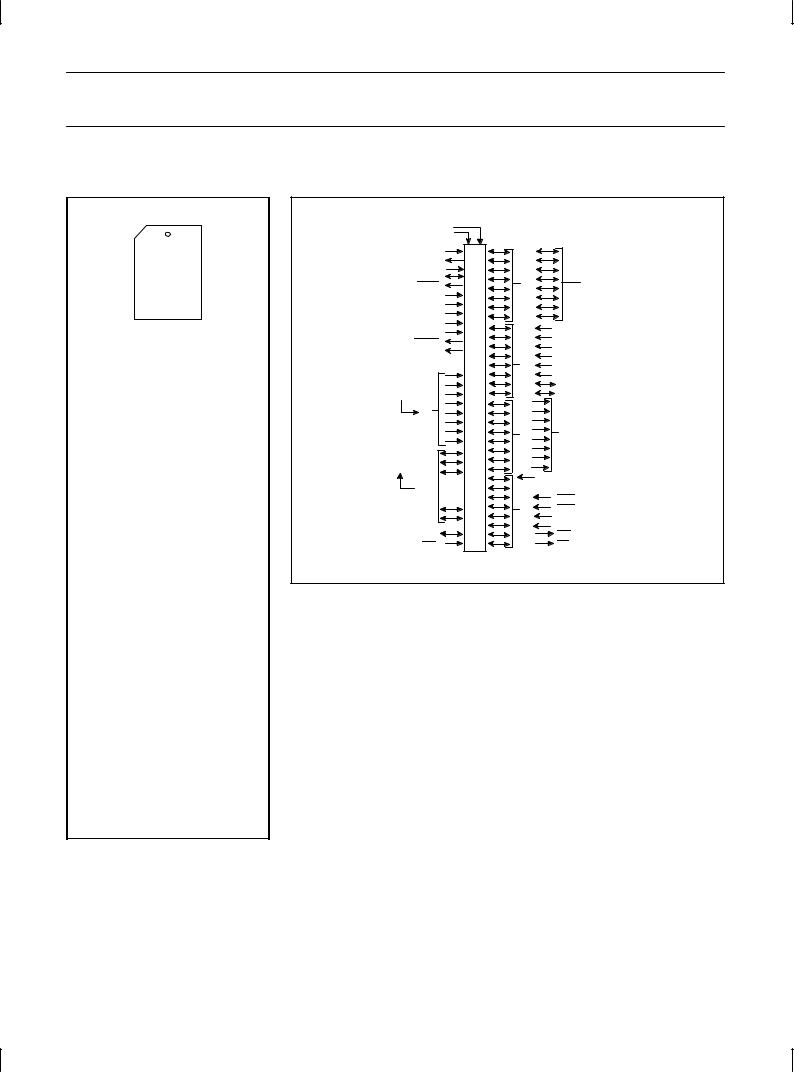
BLOCK DIAGRAM
|
T0 |
|
T1 |
|
INT0 |
INT1 |
|
|
|
|
|
|
PWM0 |
PWM1 |
AVSS |
AVREF |
ADC0-7 |
SDA |
SCL |
||
|
|
|
|
|
|
|
|
VDD |
|
VSS |
|
|
|
|
± |
+ |
|
5 |
1 |
1 |
|
|
|
3 |
3 |
|
3 |
3 |
|
|
|
|
|
AVDD |
STADC |
||||||||
|
|
|
|
|
|
|
|
|
|
|
|
|
|
|
|
|
|
|
|
||
XTAL1 |
|
|
|
|
|
|
|
|
|
|
|
|
|
|
|
|
|
|
|
|
|
|
|
T0, T1 |
|
|
|
|
|
PROGRAM |
|
|
DATA |
|
DUAL |
|
|
|
|
|
SERIAL |
||
XTAL2 |
TWO 16-BIT |
|
|
|
|
|
|
|
|
ADC |
|
|
|||||||||
TIMER/EVENT |
|
CPU |
|
MEMORY |
|
|
MEMORY |
|
PWM |
|
|
|
I2C PORT |
||||||||
|
|
|
|
|
|
|
|
|
|||||||||||||
|
COUNTERS |
|
|
|
|
8k x 8 ROM |
|
|
256 x 8 RAM |
|
|
|
|
|
|
|
|
|
|
||
EA |
|
|
|
|
|
|
|
|
|
|
|
|
|
|
|
|
|
|
|||
|
|
|
|
|
|
|
|
|
|
|
|
|
|
|
|
|
|
|
|
|
|
ALE |
|
|
80C51 CORE |
|
|
|
|
|
|
|
|
|
|
|
|
|
|
|
|
|
|
|
|
|
|
|
|
|
|
|
|
|
|
|
|
|
|
|
|
|
|
||
|
|
|
EXCLUDING |
|
|
|
|
|
|
|
|
|
|
|
|
|
|
|
|
|
|
PSEN |
|
|
ROM/RAM |
|
|
|
|
|
|
|
|
|
|
|
|
|
|
|
|
|
|
3 |
|
|
|
|
|
|
|
|
|
|
|
|
|
|
|
|
|
|
|
|
|
WR |
|
|
|
|
|
|
|
8-BIT INTERNAL BUS |
|
|
|
|
|
|
|
|
|
|
|||
|
|
|
|
|
|
|
|
|
|
|
|
|
|
|
|
|
|
||||
3 |
|
|
|
|
|
|
|
|
|
|
|
|
|
|
|
|
|
|
|
|
|
RD |
|
|
|
|
|
|
|
|
|
|
|
|
|
|
|
|
|
|
|
|
|
0 |
|
|
|
|
|
|
|
16 |
|
|
|
|
|
|
|
|
|
|
|
|
|
|
|
|
|
|
|
|
|
|
|
|
|
|
|
|
|
|
|
|
|
|
|
AD0-7 |
|
|
|
|
|
|
|
|
|
|
T2 |
|
|
T2 |
|
|
|
|
|
|
|
|
PARALLEL I/O |
|
SERIAL |
|
|
FOUR |
|
|
16 |
16-BIT |
|
COMPARA- |
|
T3 |
|
||||||
|
|
8-BIT |
|
16-BIT |
|
|
|
||||||||||||||
2 |
|
PORTS AND |
|
UART |
16-BIT |
|
TIMER/ |
COMPARA- |
|
TOR |
|
WATCHDOG |
|
||||||||
|
|
PORT |
|
|
|
|
|||||||||||||||
|
EXTERNAL BUS |
|
PORT |
CAPTURE |
|
EVENT |
|
TORS |
|
OUTPUT |
|
TIMER |
|
||||||||
|
|
|
|
|
|
|
|
|
|||||||||||||
|
|
|
|
LATCHES |
|
|
wITH |
SELECTION |
|
|
|
|
|||||||||
A8-15 |
|
|
|
|
|
|
|
|
|
COUNTERS |
|
|
|
|
|
||||||
|
|
|
|
|
|
|
|
|
|
REGISTERS |
|
|
|
|
|
|
|
||||
|
|
|
|
|
|
|
|
|
|
|
|
|
|
|
|
|
|
|
|||
|
|
|
|
|
|
|
|
|
|
|
|
|
|
|
|
|
|
|
|
||
|
|
|
|
|
3 |
3 |
|
|
|
1 |
1 |
|
1 |
|
|
|
4 |
|
|
|
|
|
P0 |
P1 |
P2 |
P3 |
TxD |
RxD |
P5 |
P4 |
CT0I-CT3I |
|
T2 |
RT2 |
|
|
CMSR0-CMSR5 RST EW |
|
|||||
|
|
|
|
|
|
|
|
|
|
|
|
|
|
|
|
CMT0, CMT1 |
|
|
|
||
0 ALTERNATE FUNCTION OF PORT 0 |
3 ALTERNATE FUNCTION OF PORT 3 |
|
|
|
|
|
|
|
|
|
|
|
|
||||||||
1 ALTERNATE FUNCTION OF PORT 1 |
4 ALTERNATE FUNCTION OF PORT 4 |
|
|
|
|
|
|
|
|
|
|
|
|
||||||||
2 ALTERNATE FUNCTION OF PORT 2 |
5 ALTERNATE FUNCTION OF PORT 5 |
|
|
|
|
|
|
|
|
|
|
|
|
||||||||
1996 Aug 06 |
6 |

Philips Semiconductors |
Product specification |
|
|
|
|
Single-chip 8-bit microcontroller |
80C552/83C552 |
|
|
|
|
PIN DESCRIPTION
|
|
|
|
|
PIN NO. |
|
|
|
|
|
|
|
|
|
|
|
|
|
|
|
|
|
|
|
|
|
MNEMONIC |
PLCC |
QFP |
TYPE |
|
|
|
|
NAME AND FUNCTION |
|||
|
|
|
|
|
|
|
|
|
|
|
|
|
|
VDD |
2 |
72 |
I |
|
Digital Power Supply: +5V power supply pin during normal operation, idle and |
||||||
|
|
|
|
|
|
|
|
|
power-down mode. |
|||
|
STADC |
3 |
74 |
I |
|
Start ADC Operation: Input starting analog to digital conversion (ADC operation can also |
||||||
|
|
|
|
|
|
|
|
|
be started by software). This pin must not float. |
|||
|
|
|
|
|
4 |
75 |
O |
|
Pulse Width Modulation: Output 0. |
|||
|
PWM0 |
|||||||||||
|
|
|
|
5 |
76 |
O |
|
Pulse Width Modulation: Output 1. |
||||
|
PWM1 |
|||||||||||
|
|
|
6 |
77 |
I |
|
Enable Watchdog Timer: Enable for T3 watchdog timer and disable power-down mode. |
|||||
|
EW |
|||||||||||
|
|
|
|
|
|
|
|
|
This pin must not float. |
|||
|
P0.0-P0.7 |
57-50 |
58-51 |
I/O |
|
Port 0: Port 0 is an 8-bit open-drain bidirectional I/O port. Port 0 pins that have 1s written |
||||||
|
|
|
|
|
|
|
|
|
to them float and can be used as high-impedance inputs. Port 0 is also the multiplexed |
|||
|
|
|
|
|
|
|
|
|
low-order address and data bus during accesses to external program and data memory. In |
|||
|
|
|
|
|
|
|
|
|
this application it uses strong internal pull-ups when emitting 1s. |
|||
|
P1.0-P1.7 |
16-23 |
10-17 |
I/O |
|
Port 1: 8-bit I/O port. Alternate functions include: |
||||||
|
|
|
|
|
16-21 |
10-15 |
I/O |
|
(P1.0-P1.5): Quasi-bidirectional port pins. |
|||
|
|
|
|
|
22-23 |
16-17 |
I/O |
|
(P1.6, P1.7): Open drain port pins. |
|||
|
|
|
|
|
16-19 |
10-13 |
I |
|
CT0I-CT3I (P1.0-P1.3): Capture timer input signals for timer T2. |
|||
|
|
|
|
|
20 |
14 |
I |
|
T2 (P1.4): T2 event input. |
|||
|
|
|
|
|
21 |
15 |
I |
|
RT2 (P1.5): T2 timer reset signal. Rising edge triggered. |
|||
|
|
|
|
|
22 |
16 |
I/O |
|
SCL (P1.6): Serial port clock line I2C-bus. |
|||
|
|
|
|
|
23 |
17 |
I/O |
|
SDA (P1.7): Serial port data line I2C-bus. |
|||
|
|
|
|
|
|
|
|
|
Port 1 is also used to input the lower order address byte during EPROM programming and |
|||
|
|
|
|
|
|
|
|
|
verification. A0 is on P1.0, etc. |
|||
|
P2.0-P2.7 |
39-46 |
38-42, |
I/O |
|
Port 2: 8-bit quasi-bidirectional I/O port. |
||||||
|
|
|
|
|
|
45-47 |
|
|
Alternate function: High-order address byte for external memory (A08-A15). |
|||
|
P3.0-P3.7 |
24-31 |
18-20, |
I/O |
|
Port 3: 8-bit quasi-bidirectional I/O port. Alternate functions include: |
||||||
|
|
|
|
|
|
23-27 |
|
|
|
|
|
|
|
|
|
|
|
24 |
18 |
|
|
RxD(P3.0): Serial input port. |
|||
|
|
|
|
|
25 |
19 |
|
|
TxD (P3.1): Serial output port. |
|||
|
|
|
|
|
26 |
20 |
|
|
|
|
|
(P3.2): External interrupt. |
|
|
|
|
|
|
|
INT0 |
|||||
|
|
|
|
|
27 |
23 |
|
|
|
|
|
(P3.3): External interrupt. |
|
|
|
|
|
|
|
INT1 |
|||||
|
|
|
|
|
28 |
24 |
|
|
T0 (P3.4): Timer 0 external input. |
|||
|
|
|
|
|
29 |
25 |
|
|
T1 (P3.5): Timer 1 external input. |
|||
|
|
|
|
|
30 |
26 |
|
|
|
|
(P3.6): External data memory write strobe. |
|
|
|
|
|
|
|
|
WR |
|||||
|
|
|
|
|
31 |
27 |
|
|
|
(P3.7): External data memory read strobe. |
||
|
|
|
|
|
|
|
RD |
|||||
|
P4.0-P4.7 |
7-14 |
80, 1-2 |
I/O |
|
Port 4: 8-bit quasi-bidirectional I/O port. Alternate functions include: |
||||||
|
|
|
|
|
|
4-8 |
|
|
|
|
|
|
|
|
|
|
|
7-12 |
80, 1-2 |
O |
|
CMSR0-CMSR5 (P4.0-P4.5): Timer T2 compare and set/reset outputs on a match with |
|||
|
|
|
|
|
|
4-6 |
|
|
timer T2. |
|||
|
|
|
|
|
13, 14 |
7, 8 |
O |
|
CMT0, CMT1 (P4.6, P4.7): Timer T2 compare and toggle outputs on a match with timer T2. |
|||
|
P5.0-P5.7 |
68-62, |
71-64, |
I |
|
Port 5: 8-bit input port. |
||||||
|
|
|
|
|
1 |
|
|
|
ADC0-ADC7 (P5.0-P5.7): Alternate function: Eight input channels to ADC. |
|||
|
RST |
15 |
9 |
I/O |
|
Reset: Input to reset the 8XC552. It also provides a reset pulse as output when timer T3 |
||||||
|
|
|
|
|
|
|
|
|
overflows. |
|||
|
XTAL1 |
35 |
32 |
I |
|
Crystal Input 1: Input to the inverting amplifier that forms the oscillator, and input to the |
||||||
|
|
|
|
|
|
|
|
|
internal clock generator. Receives the external clock signal when an external oscillator is |
|||
|
|
|
|
|
|
|
|
|
used. |
|||
|
XTAL2 |
34 |
31 |
O |
|
Crystal Input 2: Output of the inverting amplifier that forms the oscillator. Left open-circuit |
||||||
|
|
|
|
|
|
|
|
|
when an external clock is used. |
|||
|
|
|
|
|
|
|
|
|
|
|
|
|
1996 Aug 06 |
7 |

Philips Semiconductors |
Product specification |
|
|
|
|
Single-chip 8-bit microcontroller |
80C552/83C552 |
|
|
|
|
PIN DESCRIPTION (Continued)
|
|
|
|
PIN NO. |
|
|
|
|
|
|
|
|
|
|
|
|
|
|
|
|
|
|
|
|
MNEMONIC |
PLCC |
QFP |
TYPE |
|
|
NAME AND FUNCTION |
||||
|
|
|
|
|
|
|
|
|
|
|
|
|
VSS |
36, 37 |
34-36 |
I |
Two Digital ground pins. |
||||||
|
|
|
|
47 |
48 |
O |
Program Store Enable: Active-low read strobe to external program memory. |
||||
|
PSEN |
||||||||||
|
ALE |
48 |
49 |
O |
Address Latch Enable: Latches the low byte of the address during accesses to external |
||||||
|
|
|
|
|
|
|
memory. It is activated every six oscillator periods. During an external data memory |
||||
|
|
|
|
|
|
|
access, one ALE pulse is skipped. ALE can drive up to eight LS TTL inputs and handles |
||||
|
|
|
|
|
|
|
CMOS inputs without an external pull-up. |
||||
|
|
|
49 |
50 |
I |
External Access: When |
|
is held at TTL level high, the CPU executes out of the internal |
|||
|
EA |
EA |
|||||||||
|
|
|
|
|
|
|
program ROM provided the program counter is less than 8192. When EA is held at TTL |
||||
|
|
|
|
|
|
|
low level, the CPU executes out of external program memory. |
EA |
is not allowed to float. |
||
|
AVREF± |
58 |
59 |
I |
Analog to Digital Conversion Reference Resistor: Low-end. |
||||||
|
AVREF+ |
59 |
60 |
I |
Analog to Digital Conversion Reference Resistor: High-end. |
||||||
|
AVSS |
60 |
61 |
I |
Analog Ground |
||||||
|
AVDD |
61 |
63 |
I |
Analog Power Supply |
||||||
NOTE:
1. To avoid ªlatch-upº effect at power-on, the voltage on any pin at any time must not be higher or lower than V + 0.5V or V ± 0.5V,
DD SS
respectively.
OSCILLATOR CHARACTERISTICS
XTAL1 and XTAL2 are the input and output, respectively, of an inverting amplifier. The pins can be configured for use as an on-chip oscillator, as shown in the logic symbol, page 3.
To drive the device from an external clock source, XTAL1 should be driven while XTAL2 is left unconnected. There are no requirements on the duty cycle of the external clock signal, because the input to the internal clock circuitry is through a divide-by-two flip-flop. However, minimum and maximum high and low times specified in the data sheet must be observed.
RESET
A reset is accomplished by holding the RST pin high for at least two machine cycles (24 oscillator periods), while the oscillator is running. To insure a good power-on reset, the RST pin must be high long enough to allow the oscillator time to start up (normally a few milliseconds) plus two machine cycles. At power-on, the voltage on VDD and RST must come up at the same time for a proper start-up.
IDLE MODE
In the idle mode, the CPU puts itself to sleep while some of the on-chip peripherals stay active. The instruction to invoke the idle mode is the last instruction executed in the normal operating mode before the idle mode is activated. The CPU contents, the on-chip RAM, and all of the special function registers
remain intact during this mode. The idle mode can be terminated either by any enabled interrupt (at which time the process is picked up at the interrupt service routine and continued), or by a hardware reset which starts the processor in the same manner as a power-on reset.
POWER-DOWN MODE
In the power-down mode, the oscillator is stopped and the instruction to invoke power-down is the last instruction executed. Only the contents of the on-chip RAM are preserved. A hardware reset is the only way to terminate the power-down mode. The control bits for the reduced power modes are in the special function register PCON. Table 1 shows the state of the I/O ports during low current operating modes.
Table 1. External Pin Status During Idle and Power-Down Modes
MODE |
PROGRAM |
ALE |
|
|
|
PORT 0 |
PORT 1 |
PORT 2 |
PORT 3 |
PORT 4 |
PWM0/ |
MEMORY |
|
PSEN |
|
PWM1 |
|||||||
Idle |
Internal |
1 |
1 |
|
Data |
Data |
Data |
Data |
Data |
1 |
|
|
|
|
|
|
|
|
|
|
|
|
|
Idle |
External |
1 |
1 |
|
Float |
Data |
Address |
Data |
Data |
1 |
|
|
|
|
|
|
|
|
|
|
|
|
|
Power-down |
Internal |
0 |
0 |
|
Data |
Data |
Data |
Data |
Data |
1 |
|
|
|
|
|
|
|
|
|
|
|
|
|
Power-down |
External |
0 |
0 |
|
Float |
Data |
Data |
Data |
Data |
1 |
|
1996 Aug 06 |
8 |

Philips Semiconductors |
Product specification |
|
|
|
|
Single-chip 8-bit microcontroller |
80C552/83C552 |
|
|
|
|
Serial Control Register (S1CON) ± See Table 2
S1CON (D8H) |
CR2 |
ENS1 |
STA |
STO |
SI |
AA |
CR1 |
CR0 |
|
|
|
|
|
|
|
|
|
Bits CR0, CR1 and CR2 determine the serial clock frequency that is generated in the master mode of operation.
Table 2. Serial Clock Rates
|
|
|
|
BIT FREQUENCY (kHz) AT fOSC |
|
|
|
|
|||
CR2 |
CR1 |
CR0 |
6MHz |
12MHz |
16MHz |
24MHz2 |
30MHz2 |
fOSC DIVIDED BY |
|||
0 |
0 |
0 |
23 |
47 |
62.5 |
94 |
|
117 |
1 |
256 |
|
0 |
0 |
1 |
27 |
54 |
71 |
|
107 |
1 |
134 |
1 |
224 |
0 |
1 |
0 |
31 |
63 |
83.3 |
125 |
1 |
156 |
1 |
192 |
|
0 |
1 |
1 |
37 |
75 |
100 |
|
150 |
1 |
188 |
1 |
160 |
1 |
0 |
0 |
6.25 |
12.5 |
17 |
|
25 |
|
31 |
|
960 |
1 |
0 |
1 |
50 |
100 |
133 |
1 |
200 |
1 |
250 |
1 |
120 |
1 |
1 |
0 |
100 |
200 |
267 |
1 |
400 |
1 |
500 |
1 |
60 |
1 |
1 |
1 |
0.24 < 62.5 |
0.49 < 62.5 |
0.65 < 55.6 |
0.98 < 50.0 |
1.22 < 52.1 |
96 × (256 ± (reload value Timer 1)) |
|||
|
|
|
0 < 255 |
0 < 254 |
0 < 253 |
0 <251 |
0 < 250 |
reload value Timer 1 in Mode 2. |
|||
NOTES:
1.These frequencies exceed the upper limit of 100kHz of the I2C-bus specification and cannot be used in an I2C-bus application.
2.At fOSC = 24MHz/ 30MHz the maximum I2C bus rate of 100kHz cannot be realized due to the fixed divider rates.
ABSOLUTE MAXIMUM RATINGS1, 2, 3
PARAMETER |
RATING |
UNIT |
|
|
|
Storage temperature range |
±65 to +150 |
°C |
|
|
|
Voltage on any other pin to VSS |
±0.5 to +6.5 |
V |
Input, output DC current on any single I/O pin |
5.0 |
mA |
|
|
|
Power dissipation |
1.0 |
W |
(based on package heat transfer limitations, not device power consumption) |
|
|
|
|
|
NOTES:
1.Stresses above those listed under Absolute Maximum Ratings may cause permanent damage to the device. This is a stress rating only and functional operation of the device at these or any conditions other than those described in the AC and DC Electrical Characteristics section of this specification is not implied.
2.This product includes circuitry specifically designed for the protection of its internal devices from the damaging effects of excessive static charge. Nonetheless, it is suggested that conventional precautions be taken to avoid applying greater than the rated maxima.
3.Parameters are valid over operating temperature range unless otherwise specified. All voltages are with respect to VSS unless otherwise noted.
DEVICE SPECIFICATIONS
|
SUPPLY VOLTAGE (V) |
FREQUENCY (MHz) |
|
||
|
|
|
|
|
TEMPERATURE RANGE (°C) |
TYPE |
MIN |
MAX |
MIN |
MAX |
|
|
|
|
|
|
|
PCB83(0)C552-5-16 |
4.0 |
6.0 |
1.2 |
16 |
0 to +70 |
|
|
|
|
|
|
PCF83(0)C552-5-16 |
4.0 |
6.0 |
1.2 |
16 |
±40 to +85 |
|
|
|
|
|
|
PCA83(0)C552-5-16 |
4.5 |
5.5 |
1.2 |
16 |
±40 to +125 |
|
|
|
|
|
|
PCB83(0)C552-5-24 |
4.5 |
5.5 |
1.2 |
24 |
0 to +70 |
|
|
|
|
|
|
PCF83(0)C552-5-24 |
4.5 |
5.5 |
1.2 |
24 |
±40 to +85 |
|
|
|
|
|
|
PCB83(0)C552-5-30 |
4.5 |
5.5 |
1.2 |
30 |
0 to +70 |
|
|
|
|
|
|
1996 Aug 06 |
9 |
 Loading...