


Philips PCF8579H-F1, PCF8579U, PCF8579U-10, PCF8579U-12, PCF8579U-2-F1 Datasheet
...INTEGRATED CIRCUITS
DATA SHEET
PCF8579
LCD column driver for dot matrix graphic displays
Product specification |
1997 Apr 01 |
Supersedes data of 1996 Oct 25
File under Integrated Circuits, IC12

Philips Semiconductors Product specification
|
LCD column driver for dot matrix graphic |
PCF8579 |
||
|
displays |
|
||
|
|
|
||
|
|
|
||
|
|
|
||
CONTENTS |
10 |
LIMITING VALUES |
||
1 |
FEATURES |
11 |
HANDLING |
|
12 |
DC CHARACTERISTICS |
|||
2 |
APPLICATIONS |
|||
13 |
AC CHARACTERISTICS |
|||
3 |
GENERAL DESCRIPTION |
|||
14 |
APPLICATION INFORMATION |
|||
4 |
ORDERING INFORMATION |
|||
15 |
CHIP DIMENSIONS AND BONDING PAD |
|||
5 |
BLOCK DIAGRAM |
|||
|
LOCATIONS |
|||
6 |
PINNING |
|
||
16 |
CHIP-ON GLASS INFORMATION |
|||
7 |
FUNCTIONAL DESCRIPTION |
|||
17 |
PACKAGE OUTLINES |
|||
|
|
|||
7.1Multiplexed LCD bias generation
7.2Power-on reset
7.3Timing generator
7.4Column drivers
7.5Display RAM
7.6Data pointer
7.7Subaddress counter
7.8I2C-bus controller
7.9Input filters
7.10RAM access
7.11Display control
7.12TEST pin
8 |
I2C-BUS PROTOCOL |
8.1Command decoder
18 SOLDERING
18.1Introduction
18.2Reflow soldering
18.3Wave soldering
18.3.1LQFP
18.3.2VSO
18.3.3Method (LQFP and VSO)
18.4Repairing soldered joints
19DEFINITIONS
20LIFE SUPPORT APPLICATIONS
21PURCHASE OF PHILIPS I2C COMPONENTS
9 |
CHARACTERISTICS OF THE I2C-BUS |
9.1Bit transfer
9.2Start and stop conditions
9.3System configuration
9.4Acknowledge
1997 Apr 01 |
2 |
|
|
|
|
|
|
||
|
|
|
||
|
|
|
||
|
|
|
||
|
|
|

Philips Semiconductors |
Product specification |
|
|
LCD column driver for dot matrix graphic
PCF8579
displays
1 FEATURES
∙LCD column driver
∙Used in conjunction with the PCF8578, this device forms part of a chip set capable of driving up to 40960 dots
∙40 column outputs
∙Selectable multiplex rates; 1 : 8, 1 : 16, 1 : 24 or 1 : 32
∙Externally selectable bias configuration, 5 or 6 levels
∙Easily cascadable for large applications (up to 32 devices)
∙1280-bit RAM for display data storage
∙Display memory bank switching
∙Auto-incremented data loading across hardware subaddress boundaries (with PCF8578)
∙Power-on reset blanks display
∙Logic voltage supply range 2.5 to 6 V
∙Maximum LCD supply voltage 9 V
∙Low power consumption
∙I2C-bus interface
∙TTL/CMOS compatible
∙Compatible with most microcontrollers
∙Optimized pinning for single plane wiring in multiple device applications (with PCF8578)
∙Space saving 56-lead plastic mini-pack and 64-pin plastic low profile quad flat package
∙Compatible with chip-on-glass technology
∙I2C-bus address: 011110 SA0.
2 APPLICATIONS
∙Automotive information systems
∙Telecommunication systems
∙Point-of-sale terminals
∙Computer terminals
∙Instrumentation.
3 GENERAL DESCRIPTION
The PCF8579 is a low power CMOS LCD column driver, designed to drive dot matrix graphic displays at multiplex rates of 1 : 8, 1 : 16, 1 : 24 or 1 : 32. The device has
40 outputs and can drive 32 × 40 dots in a 32 row multiplexed LCD. Up to 16 PCF8579s can be cascaded and up to 32 devices may be used on the same I2C-bus (using the two slave addresses). The device is optimized for use with the PCF8578 LCD row/column driver. Together these two devices form a general purpose LCD dot matrix driver chip set, capable of driving displays of up to 40960 dots. The PCF8579 is compatible with most microcontrollers and communicates via a two-line bidirectional bus (I2C-bus). To allow partial VDD shutdown the ESD protection system of the SCL and SDA pins does not use a diode connected to VDD. Communication overheads are minimized by a display RAM with auto-incremented addressing and display bank switching.
4 ORDERING INFORMATION
TYPE |
|
PACKAGE |
|
|
|
|
|
NUMBER |
NAME |
DESCRIPTION |
VERSION |
|
|||
|
|
|
|
PCF8579T |
VSO56 |
plastic very small outline package; 56 leads |
SOT190 |
|
|
|
|
PCF8579U7 |
− |
chip with bumps on tape |
− |
|
|
|
|
PCF8579H |
LQFP64 |
plastic low profile quad flat package; 64 leads; body 10 × 10 × 1.4 mm |
SOT314-2 |
|
|
|
|
1997 Apr 01 |
3 |
Philips Semiconductors |
Product specification |
|
|
LCD column driver for dot matrix graphic
PCF8579
displays
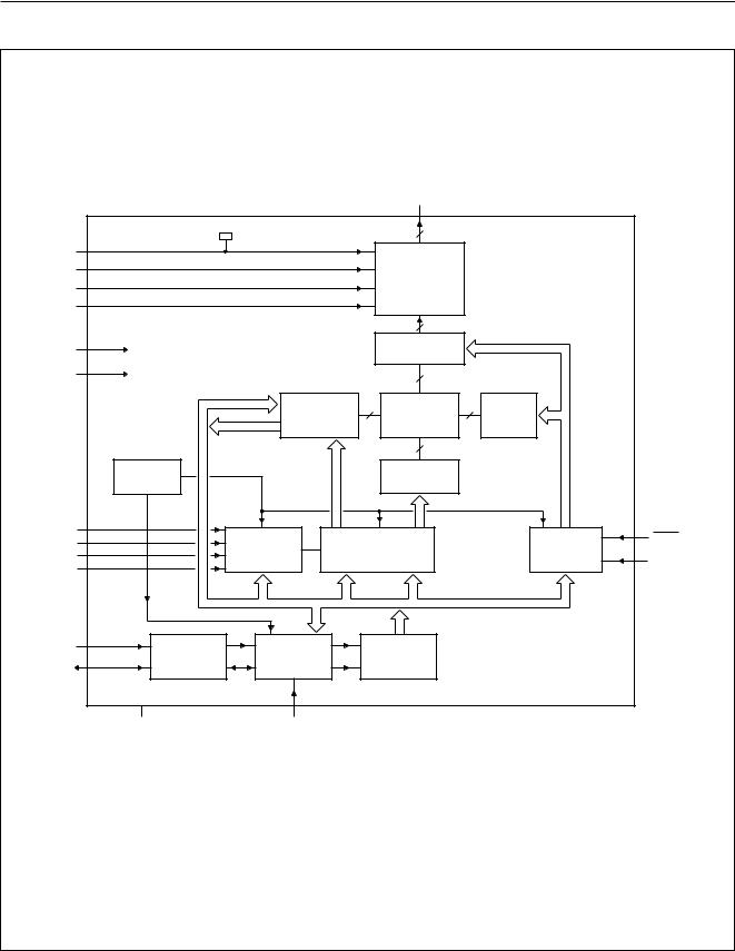
5 BLOCK DIAGRAM
|
|
|
|
|
C39 - C0 |
|
|
|
|
|
|
|
17 - 56 |
|
|
|
|
|
|
|
(30 to 33, 35 to 64, 1 to 6) |
|
|
VDD |
12 (20) |
|
|
|
|
|
|
14 (22) |
|
|
|
|
|
|
|
V3 |
|
|
|
COLUMN (1) |
|
|
|
15 (23) |
|
|
|
PCF8579 |
|
||
V4 |
|
|
|
DRIVERS |
|
||
16 (24) |
|
|
|
|
|
||
VLCD |
|
|
|
|
|
|
|
|
|
|
|
|
|
|
|
TEST |
6 (12) |
|
|
|
OUTPUT |
|
|
|
|
|
|
CONTROLLER |
|
|
|
|
|
|
|
|
|
|
|
VSS |
5 (11) |
|
|
|
|
|
|
|
|
|
|
|
|
|
|
|
|
|
Y DECODER |
32 x 40 BIT |
DISPLAY |
|
|
|
|
|
AND SENSING |
|
|||
|
|
|
DISPLAY RAM |
DECODER |
|
||
|
|
|
AMPLIFIERS |
|
|||
|
|
|
|
|
|
||
|
POWER-ON |
|
|
X DECODER |
|
|
|
|
|
RESET |
|
|
|
|
|
|
|
|
|
|
|
|
|
A3 |
8 (14) |
|
|
|
|
|
(9) 3 |
9 (16) |
|
|
|
|
|
||
A2 |
|
SUBADDRESS |
|
|
TIMING |
SYNC |
|
10 (17) |
|
RAM DATA POINTER |
(10) 4 |
||||
A1 |
|
COUNTER |
GENERATOR |
||||
11 (18) |
|
Y |
X |
CLK |
|||
A0 |
|
|
|
||||
|
|
|
|
|
|||
|
|
|
|
|
|
|
|
SCL |
2 (8) |
|
I2C-BUS |
|
|
|
|
1 (7) |
INPUT |
|
COMMAND |
|
|
||
SDA |
FILTERS |
CONTROLLER |
|
DECODER |
|
|
|
|
|
|
|
|
|
|
|
|
|
(15, 19, 21, 25 to 29, 34) |
|
|
|
|
|
|
|
13 |
7 (13) |
|
|
|
|
|
|
n.c. |
|
|
|
|
MSA919 |
|
|
SA0 |
|
|
|
|
|
(1) Operates at LCD voltage levels, all other blocks operate at logic levels. The pin numbers given in parenthesis refer to the LQFP64 package.
Fig.1 Block diagram.
1997 Apr 01 |
4 |

Philips Semiconductors |
Product specification |
|
|
LCD column driver for dot matrix graphic
PCF8579
displays
6 PINNING
|
SYMBOL |
|
PINS |
DESCRIPTION |
||
|
|
|
|
|||
|
VSO56 |
|
LQFP64 |
|||
|
|
|
|
|
||
|
|
|
|
|
|
|
|
SDA |
1 |
|
7 |
I2C-bus serial data input/output |
|
|
SCL |
2 |
|
8 |
I2C-bus serial clock input |
|
|
|
|
3 |
|
9 |
cascade synchronization input |
|
SYNC |
|
|
|||
|
|
|
|
|
|
|
|
CLK |
4 |
|
10 |
external clock input |
|
|
|
|
|
|
|
|
|
VSS |
5 |
|
11 |
ground (logic) |
|
|
TEST |
6 |
|
12 |
test pin (connect to VSS) |
|
|
SA0 |
7 |
|
13 |
I2C-bus slave address input (bit 0) |
|
|
A3 to A0 |
8 to 11 |
|
14, 16 to 18 |
I2C-bus subaddress inputs |
|
|
VDD |
12 |
|
20 |
supply voltage |
|
|
n.c. |
13(1) |
|
15, 19, 21,25 to 29, 34 |
not connected |
|
|
V3, V4 |
14 and 15 |
|
22 and 23 |
LCD bias voltage inputs |
|
|
VLCD |
16 |
|
24 |
LCD supply voltage |
|
|
C39 to C0 |
17 to 56 |
|
30 to 33, 35 to 64 and 1 to 6 |
LCD column driver outputs |
|
|
|
|
|
|
|
|
Note
1. Do not connect, this pin is reserved.
1997 Apr 01 |
5 |

Philips Semiconductors |
Product specification |
|
|
LCD column driver for dot matrix graphic
PCF8579
displays
SDA |
|
|
|
C0 |
|
1 |
|
56 |
|||
|
|
2 |
|
|
|
SCL |
|
55 |
C1 |
||
|
|
|
|
|
|
SYNC |
3 |
|
54 |
C2 |
|
CLK |
|
|
|
C3 |
|
4 |
|
53 |
|||
VSS |
|
|
|
C4 |
|
5 |
|
52 |
|||
TEST |
|
|
|
C5 |
|
6 |
|
51 |
|||
SA0 |
|
|
|
|
|
7 |
|
50 |
C6 |
||
A3 |
|
|
|
|
|
8 |
|
49 |
C7 |
||
A2 |
|
|
|
C8 |
|
9 |
|
48 |
|||
A1 |
|
|
|
|
|
10 |
|
47 |
C9 |
||
|
|
|
|
|
|
A0 |
11 |
|
46 |
C10 |
|
V DD |
12 |
|
|
|
|
|
45 |
C11 |
|||
n.c. |
13 |
|
44 |
C12 |
|
V 3 |
14 |
PCF8579 |
43 |
C13 |
|
V 4 |
|
|
|
||
15 |
|
42 |
C14 |
||
V LCD |
|
|
|
|
|
16 |
|
41 |
C15 |
||
|
|
|
|
40 |
|
C39 |
17 |
|
C16 |
||
C38 |
|
|
39 |
|
|
18 |
|
C17 |
|||
|
|
|
|
|
|
C37 |
19 |
|
38 |
C18 |
|
|
|
|
|
|
|
C36 |
20 |
|
37 |
C19 |
|
|
|
|
|
|
|
C35 |
21 |
|
36 |
C20 |
|
|
|
|
|
|
|
C34 |
22 |
|
35 |
C21 |
|
C33 |
|
|
|
|
|
23 |
|
34 |
C22 |
||
|
|
|
|
|
|
C32 |
24 |
|
33 |
C23 |
|
C31 |
|
|
|
|
|
25 |
|
32 |
C24 |
||
|
|
|
|
|
|
C30 |
26 |
|
31 |
C25 |
|
C29 |
|
|
|
|
|
27 |
|
30 |
C26 |
||
C28 |
28 |
|
|
|
|
|
29 |
C27 |
|||
|
|
|
|
|
|
|
|
|
MSA918 |
|
|
Fig.2 Pin configuration (VSO56).
1997 Apr 01 |
6 |

Philips Semiconductors |
Product specification |
|
|
LCD column driver for dot matrix graphic
PCF8579
displays
handbook, full pagewidth
C6 |
|
C7 |
|
C8 |
|
C9 |
|
C10 |
|
C11 |
|
C12 |
|
C13 |
|
C14 |
|
C15 |
|
C16 |
|
C17 |
|
C18 |
|
C19 |
|
C20 |
|
C21 |
|
|
|
|
|
|
|
|
|
|
|
|
|
|
|
|
|
|
|
|
|
|
|
|
|
|
|
|
|
|
|
64 |
|
63 |
|
62 |
|
61 |
|
60 |
|
59 |
|
58 |
|
57 |
|
56 |
|
55 |
|
54 |
|
53 |
|
52 |
|
51 |
|
50 |
|
49 |
|
|
|
|
|
|
|
|
|
|
|
|
|
|
|
|
|
|
|
|
|
|
|
|
|
|
|
|
|
|
|
C5 1
C4 2
C3 3
C2 4
C1 5
C0 6
SDA 7
SCL 8
PCF8579
SYNC 9
CLK 10
VSS 11
TEST 12
SA0 13
A3 14
n.c. 15 A2 16
17 |
|
18 |
|
19 |
|
20 |
|
21 |
|
22 |
|
23 |
|
24 |
|
25 |
|
26 |
|
27 |
|
28 |
|
29 |
|
30 |
|
31 |
|
32 |
|
|
|
|
|
|
|
|
|
|
|
|
|
|
|
|
|
|
|
|
|
|
|
|
|
|
|
|
|
|
|
A1 |
|
A0 |
|
n.c. |
|
DD |
|
n.c. |
3 |
4 |
|
LCD |
|
n.c. |
|
n.c. |
|
n.c. |
|
n.c. |
|
n.c. |
|
C39 |
|
C38 |
|
C37 |
||
|
|
|
V |
|
|
V |
|
V |
|
V |
|
|
|
|
|
|
|
|
||||||||||||
48 C22
47 C23
46 C24
45 C25
44 C26
43 C27
42 C28
41 C29
40 C30
39 C31
38 C32
37 C33
36 C34
35 C35
34 n.c.
33 C36
MBH590
Fig.3 Pin configuration (LQFP64).
1997 Apr 01 |
7 |
Philips Semiconductors |
Product specification |
|
|
LCD column driver for dot matrix graphic
PCF8579
displays
7 FUNCTIONAL DESCRIPTION
The PCF8579 column driver is designed for use with the PCF8578. Together they form a general purpose LCD dot matrix chip set.
Typically up to 16 PCF8579s may be used with one PCF8578. Each of the PCF8579s is identified by a unique 4-bit hardware subaddress, set by pins A0 to A3.
The PCF8578 can operate with up to 32 PCF8579s when using two I2C-bus slave addresses. The two slave addresses are set by the logic level on input SA0.
7.1Multiplexed LCD bias generation
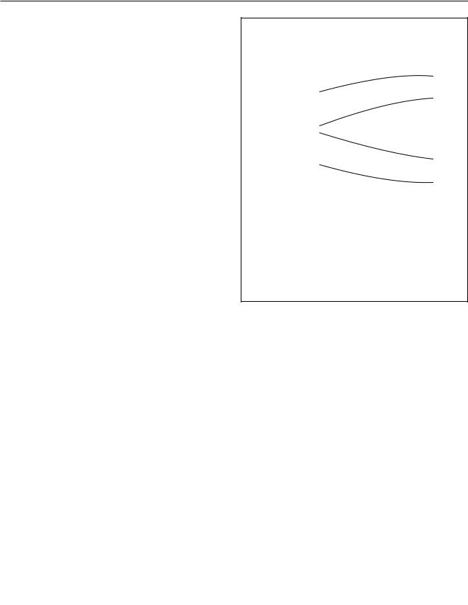
The bias levels required to produce maximum contrast depend on the multiplex rate and the LCD threshold voltage (Vth). Vth is typically defined as the RMS voltage at which the LCD exhibits 10% contrast. Table 1 shows the optimum voltage bias levels for the PCF8578/PCF8579
chip set as functions of Vop (Vop = VDD − VLCD), together with the discrimination ratios (D) for the different multiplex
rates. A practical value for Vop is obtained by equating
Voff(rms) with Vth. Figure 4 shows the first 4 rows of Table 1 as graphs.
Table 1 Optimum LCD bias voltages
PARAMETER |
|
MULTIPLEX RATE |
|
||
|
|
|
|
||
1 : 8 |
1 : 16 |
1 : 24 |
1 : 32 |
||
|
|||||
|
|
|
|
|
|
V2 |
0.739 |
0.800 |
0.830 |
0.850 |
|
--------- |
|||||
Vop |
|
|
|
|
|
V3 |
0.522 |
0.600 |
0.661 |
0.700 |
|
--------- |
|||||
Vop |
|
|
|
|
|
V4 |
0.478 |
0.400 |
0.339 |
0.300 |
|
--------- |
|||||
Vop |
|
|
|
|
|
V5 |
0.261 |
0.200 |
0.170 |
0.150 |
|
--------- |
|||||
Vop |
|
|
|
|
|
Voff ( rms) |
0.297 |
0.245 |
0.214 |
0.193 |
|
----------------------- |
|||||
Vop |
|
|
|
|
|
Von ( rms) |
0.430 |
0.316 |
0.263 |
0.230 |
|
---------------------- |
|||||
Vop |
|
|
|
|
|
Von ( rms) |
1.447 |
1.291 |
1.230 |
1.196 |
|
D = ----------------------- |
|||||
Voff ( rms) |
|
|
|
|
|
Vop |
3.370 |
4.080 |
4.680 |
5.190 |
|
--------- |
|||||
Vth |
|
|
|
|
|
MSA838
1.0 |
|
|
|
|
|
|
|
|
|
|
|
|
|
|
|
|
|
|
|
||
V bias |
|
|
|
|
|
|
|
|
|
|
Vop |
|
|
|
|
|
V2 |
|
|
|
|
0.8 |
|
|
|
|
|
|
|
|
|
|
|
|
|
|
|
|
|
|
|
||
|
|
|
|
|
|
|
|
|
|
|
|
|
|
|
|
|
V3 |
|
|
|
|
0.6 |
|
|
|
|
|
|
|
|
|
|
|
|
|
|
|
|
|
|
|
||
0.4 |
|
|
|
|
|
|
|
|
|
|
|
|
|
|
|
|
|
|
|
||
|
|
|
|
V4 |
|
|
|
|
||
|
|
|
|
|
|
|
|
|
|
|
0.2 |
|
|
|
|
|
|
|
|
|
|
|
|
|
|
V5 |
|
|
|
|
||
|
|
|
|
|
|
|
|
|
|
|
0 |
|
|
|
|
|
|
|
|
|
|
|
|
|
|
|
|
|
|
|
||
1:8 |
1:16 |
1:24 |
1:32 |
|||||||
multiplex rate
Vbias = V2, V3, V4, V5. See Table 1.
Fig.4 Vbias/Vop as a function of the multiplex rate.
7.2Power-on reset
At power-on the PCF8579 resets to a defined starting condition as follows:
1.Display blank (in conjunction with PCF8578)
2.1 : 32 multiplex rate
3.Start bank, 0 selected
4.Data pointer is set to X, Y address 0, 0
5.Character mode
6.Subaddress counter is set to 0
7.I2C-bus is initialized.
Data transfers on the I2C-bus should be avoided for 1 ms following power-on, to allow completion of the reset action.
1997 Apr 01 |
8 |

Philips Semiconductors |
Product specification |
|
|
LCD column driver for dot matrix graphic
PCF8579
displays
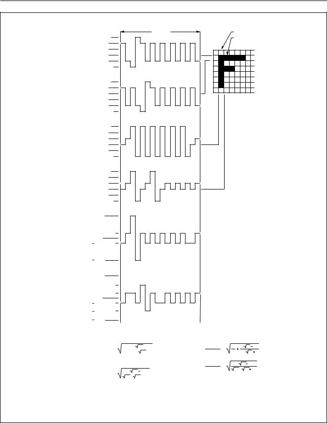
T frame
0 |
1 |
2 |
3 |
4 |
5 |
6 |
7 |
VDD
V 2
V3
ROW 0 V4
V5
VLCD
VDD
V 2
V3
COLUMN V4
V5
VLCD
SYNC 


0 |
1 |
2 |
3 |
4 |
5 |
6 |
7 |
8 |
9 |
10 |
11 |
12 |
13 |
14 |
15 |
VDD
V 2
V3
ROW 0 V4
V5
VLCD
VDD
V 2
V3
COLUMN V4
V5
VLCD
SYNC 


0 |
1 |
2 |
3 |
4 |
5 |
6 |
7 |
8 |
9 |
10 |
11 |
12 |
13 |
14 |
15 |
16 |
17 |
18 |
19 |
20 |
21 |
22 |
23 |
VDD
V 2
V3
ROW 0 V4
V5
VLCD
VDD
V 2
V3
COLUMN V4
V5
VLCD
SYNC 

0 1 2 3 4 5 6 7 8 9 10 11 12 13 14 15 16 17 18 19 20 21 22 23 24 25 26 27 28 29 30 31
VDD
V 2
V3 ROW 0 V4
V5
VLCD
VDD
V 2
V3
COLUMN V4
V5
VLCD
SYNC 


MSA841
ON
OFF
1:8
1:16
1:24
1:32
column display
Fig.5 LCD row/column waveforms.
1997 Apr 01 |
9 |
Philips Semiconductors |
Product specification |
|
|
LCD column driver for dot matrix graphic
PCF8579
displays
ROW 1
R1 (t)
ROW 2
R2 (t)
COL 1
C1 (t)
COL 2
C2 (t)
V state 1 (t)
V state 2 (t)
T frame
VDD
V2
V3 V4 V5
VLCD
VDD
V2
V3
V4
V5
VLCD
VDD
V2
V3
V4
V5
VLCD
VDD
V2
V3
V4
V5
VLCD
Vop
0.261 Vop
0 V
0.261 Vop
Vop
Vop
0.478 Vop
0.261 Vop
0 V
0.261 Vop
0.478 Vop
Vop
Vstate 1 |
(t) = C1(t) |
|
R1(t): |
|
|
|||||||||
|
|
|
||||||||||||
Von(rms) |
= |
1 |
|
|
|
8 |
|
|
1 |
|
= 0.430 |
|||
|
|
|
|
|
||||||||||
Vop |
|
8 |
|
|
|
8 ( |
8 |
|
|
|
1) |
|||
Vstate 2 |
(t) = C2(t) |
|
R2(t): |
|
|
|||||||||
|
|
|
||||||||||||
|
Voff(rms) |
= |
2 ( 8 |
1) |
= 0.297 |
|||
|
8 ( |
|
|
|
1) 2 |
|||
|
Vop |
8 |
|
|
|
|||
state 1 (OFF)
state 2 (ON)
dot matrix
1:8 multiplex rate
MSA840
general relationship (n = multiplex rate)
Von(rms) = |
1 |
n ( |
n |
1 |
||
Vop |
|
n |
n |
1) |
||
Voff(rms) |
= |
2 ( |
n |
1) |
||
Vop |
n ( |
n |
1) 2 |
|||
|
||||||
Fig.6 LCD drive mode waveforms for 1 : 8 multiplex rate.
1997 Apr 01 |
10 |
Philips Semiconductors |
Product specification |
|
|
LCD column driver for dot matrix graphic
PCF8579
displays
ROW 1
R1 (t)
ROW 2
R2 (t)
COL 1
C1 (t)
COL 2
C2 (t)
V state 1 (t)
V state 2 (t)
|
|
|
|
|
|
|
|
|
|
|
|
|
|
|
|
|
|
|
|
T frame |
|
|
|
|
|
|
|
|
|
|
|
|
|
|
|
|
|
|
|
|
|
|
|
state 1 (OFF) |
|||||||
|
|
|
|
|
|
|
|
|
|
|
|
|
|
|
|
|
|
|
|
|
|
|
|
|
|
|
|
|
|
|
|
|
|
|
|
|
|
|
|
|
|
|
|||||||||
VDD |
|
|
|
|
|
|
|
|
|
|
|
|
|
|
|
|
|
|
|
|
|
|
|
|
|
|
|
state 2 (ON) |
|||||||||||||||||||||||
|
|
|
|
|
|
|
|
|
|
|
|
|
|
|
|
|
|
|
|
|
|
|
|
|
|
|
|
|
|
|
|
|
|
|
|
|
|
|
|
|
|
|
|
||||||||
|
|
|
|
|
|
|
|
|
|
|
|
|
|
|
|
|
|
|
|
|
|
|
|
|
|
|
|
|
|
|
|
|
|
|
|
|
|
|
|
|
|
|
|
|
|
|
|
|
|||
V2 |
|
|
|
|
|
|
|
|
|
|
|
|
|
|
|
|
|
|
|
|
|
|
|
|
|
|
|
|
|
|
|
|
|
|
|
|
|
|
|
|
|
|
|
|
|
|
|
|
|
|
|
|
|
|
|
|
|
|
|
|
|
|
|
|
|
|
|
|
|
|
|
|
|
|
|
|
|
|
|
|
|
|
|
|
|
|
|
|
|
|
|
|
|
|
|
|
|
|
|
|
|
||
V3 |
|
|
|
|
|
|
|
|
|
|
|
|
|
|
|
|
|
|
|
|
|
|
|
|
|
|
|
|
|
|
|
|
|
|
|
|
|
|
|
|
|
|
|
|
|
|
|
|
|
||
|
|
|
|
|
|
|
|
|
|
|
|
|
|
|
|
|
|
|
|
|
|
|
|
|
|
|
|
|
|
|
|
|
|
|
|
|
|
|
|
|
|
|
|
|
|
|
|
|
|
||
V4 |
|
|
|
|
|
|
|
|
|
|
|
|
|
|
|
|
|
|
|
|
|
|
|
|
|
|
|
|
|
|
|
|
|
|
|
|
|
|
|
|
|
|
|
|
|
|
|
|
|
||
|
|
|
|
|
|
|
|
|
|
|
|
|
|
|
|
|
|
|
|
|
|
|
|
|
|
|
|
|
|
|
|
|
|
|
|
|
|
|
|
|
|
|
|
|
|
|
|
|
|||
V5 |
|
|
|
|
|
|
|
|
|
|
|
|
|
|
|
|
|
|
|
|
|
|
|
|
|
|
|
|
|
|
|
|
|
|
|
|
|
|
|
|
|
|
|
|
|
|
|
|
|
||
|
|
|
|
|
|
|
|
|
|
|
|
|
|
|
|
|
|
|
|
|
|
|
|
|
|
|
|
|
|
|
|
|
|
|
|
|
|
|
|
|
|
|
|
|
|
|
|
|
|
||
VLCD |
|
|
|
|
|
|
|
|
|
|
|
|
|
|
|
|
|
|
|
|
|
|
|
|
|
|
|
|
|
|
|
|
|
|
|
|
|
|
|
|
|
|
|
|
|
|
|
|
|||
|
|
|
|
|
|
|
|
|
|
|
|
|
|
|
|
|
|
|
|
|
|
|
|
|
|
|
|
|
|
|
|
|
|
|
|
|
|
|
|
|
|
|
|
|
|
|
|
||||
VDD |
|
|
|
|
|
|
|
|
|
|
|
|
|
|
|
|
|
|
|
|
|
|
|
|
|
|
|
|
|
|
|
|
|
|
|
|
|
|
|
|
|
|
|
|
|
|
|
|
|
||
|
|
|
|
|
|
|
|
|
|
|
|
|
|
|
|
|
|
|
|
|
|
|
|
|
|
|
|
|
|
|
|
|
|
|
|
|
|
|
|
|
|
|
|
|
|
|
|
|
|||
|
|
|
|
|
|
|
|
|
|
|
|
|
|
|
|
|
|
|
|
|
|
|
|
|
|
|
|
|
|
|
|
|
|
|
|
|
|
|
|
|
|
|
|
|
|
|
|
|
|||
V2 |
|
|
|
|
|
|
|
|
|
|
|
|
|
|
|
|
|
|
|
|
|
|
|
|
|
|
|
|
|
|
|
|
|
|
|
|
|
|
|
|
|
|
|
|
|
|
|
|
|
|
|
V3 |
|
|
|
|
|
|
|
|
|
|
|
|
|
|
|
|
|
|
|
|
|
|
|
|
|
|
|
|
|
|
|
|
|
|
|
|
|
|
|
|
|
|
|
|
|
|
|
|
|
|
|
|
|
|
|
|
|
|
|
|
|
|
|
|
|
|
|
|
|
|
|
|
|
|
|
|
|
|
|
|
|
|
|
|
|
|
|
|
|
|
|
|
|
|
|
|
|
|
|
||||
V4 |
|
|
|
|
|
|
|
|
|
|
|
|
|
|
|
|
|
|
|
|
|
|
|
|
|
|
|
|
|
|
|
|
|
|
|
|
|
|
|
|
|
|
|
|
|
|
|
|
|
|
|
|
|
|
|
|
|
|
|
|
|
|
|
|
|
|
|
|
|
|
|
|
|
|
|
|
|
|
|
|
|
|
|
|
|
|
|
|
|
|
|
|
|
|
|
|
|
|
|
||||
V5 |
|
|
|
|
|
|
|
|
|
|
|
|
|
|
|
|
|
|
|
|
|
|
|
|
|
|
|
|
|
|
|
|
|
|
|
|
|
|
|
|
|
|
|
|
|
|
|
|
|
|
|
VLCD |
|
|
|
|
|
|
|
|
|
|
|
|
|
|
|
|
|
|
|
|
|
|
|
|
|
|
|
|
|
|
|
|
|
|
|
|
|
|
|
|
|
|
|
|
|
|
|
|
|||
|
|
|
|
|
|
|
|
|
|
|
|
|
|
|
|
|
|
|
|
|
|
|
|
|
|
|
|
|
|
|
|
|
|
|
|
|
|
|
|
|
|
|
|
|
|
|
|
||||
VDD |
|
|
|
|
|
|
|
|
|
|
|
|
|
|
|
|
|
|
|
|
|
|
|
|
|
|
|
|
|
|
|
|
|
|
|
|
|
|
|
|
|
|
|
|
|
|
|
|
|
||
|
|
|
|
|
|
|
|
|
|
|
|
|
|
|
|
|
|
|
|
|
|
|
|
|
|
|
|
|
|
|
|
|
|
|
|
|
|
|
|
|
|
|
|
|
|
|
|
|
|||
|
|
|
|
|
|
|
|
|
|
|
|
|
|
|
|
|
|
|
|
|
|
|
|
|
|
|
|
|
|
|
|
|
|
|
|
|
|
|
|
|
|
|
|
|
|
|
|
|
|||
V2 |
|
|
|
|
|
|
|
|
|
|
|
|
|
|
|
|
|
|
|
|
|
|
|
|
|
|
|
|
|
|
|
|
|
|
|
|
|
|
|
|
|
|
|
|
|
|
|
|
|||
|
|
|
|
|
|
|
|
|
|
|
|
|
|
|
|
|
|
|
|
|
|
|
|
|
|
|
|
|
|
|
|
|
|
|
|
|
|
|
|
|
|
|
|
|
|
|
|
||||
V3 |
|
|
|
|
|
|
|
|
|
|
|
|
|
|
|
|
|
|
|
|
|
|
|
|
|
|
|
|
|
|
|
|
|
|
|
|
|
|
|
|
|
|
|
|
|
|
|
|
|
|
|
|
|
|
|
|
|
|
|
|
|
|
|
|
|
|
|
|
|
|
|
|
|
|
|
|
|
|
|
|
|
|
|
|
|
|
|
|
|
|
|
|
|
|
|
|
|
|
|
|
|
||
V4 |
|
|
|
|
|
|
|
|
|
|
|
|
|
|
|
|
|
|
|
|
|
|
|
|
|
|
|
|
|
|
|
|
|
|
|
|
|
|
|
|
|
|
|
|
|
|
|
|
|
|
|
|
|
|
|
|
|
|
|
|
|
|
|
|
|
|
|
|
|
|
|
|
|
|
|
|
|
|
|
|
|
|
|
|
|
|
|
|
|
|
|
|
|
|
|
|
|
|
|
|
|
||
V5 |
|
|
|
|
|
|
|
|
|
|
|
|
|
|
|
|
|
|
|
|
|
|
|
|
|
|
|
|
|
|
|
|
|
|
|
|
|
|
|
|
|
|
dot matrix |
||||||||
|
|
|
|
|
|
|
|
|
|
|
|
|
|
|
|
|
|
|
|
|
|
|
|
|
|
|
|
|
|
|
|
|
|
|
|
|
|
|
|
||||||||||||
VLCD |
|
|
|
|
|
|
|
|
|
|
|
|
|
|
|
|
|
|
|
|
|
|
|
|
|
|
|
|
|
|
|
|
|
|
|
|
|
|
|
|
1:16 multiplex rate |
||||||||||
|
|
|
|
|
|
|
|
|
|
|
|
|
|
|
|
|
|
|
|
|
|
|
|
|
|
|
|
|
|
|
|
|
|
|
|
|
|
|
|
||||||||||||
VDD |
|
|
|
|
|
|
|
|
|
|
|
|
|
|
|
|
|
|
|
|
|
|
|
|
|
|
|
|
|
|
|
|
|
|
|
|
|
|
|
|
|
|
|
|
|
|
|
|
|||
|
|
|
|
|
|
|
|
|
|
|
|
|
|
|
|
|
|
|
|
|
|
|
|
|
|
|
|
|
|
|
|
|
|
|
|
|
|
|
|
|
|
|
|
|
|
|
|
|
|||
V2 |
|
|
|
|
|
|
|
|
|
|
|
|
|
|
|
|
|
|
|
|
|
|
|
|
|
|
|
|
|
|
|
|
|
|
|
|
|
|
|
|
|
|
|
|
|
|
|
|
|||
|
|
|
|
|
|
|
|
|
|
|
|
|
|
|
|
|
|
|
|
|
|
|
|
|
|
|
|
|
|
|
|
|
|
|
|
|
|
|
|
|
|
|
|
|
|
|
|
||||
V3 |
|
|
|
|
|
|
|
|
|
|
|
|
|
|
|
|
|
|
|
|
|
|
|
|
|
|
|
|
|
|
|
|
|
|
|
|
|
|
|
|
|
|
|
|
|
|
|
|
|||
|
|
|
|
|
|
|
|
|
|
|
|
|
|
|
|
|
|
|
|
|
|
|
|
|
|
|
|
|
|
|
|
|
|
|
|
|
|
|
|
|
|
|
|
|
|
|
|
|
|
||
|
|
|
|
|
|
|
|
|
|
|
|
|
|
|
|
|
|
|
|
|
|
|
|
|
|
|
|
|
|
|
|
|
|
|
|
|
|
|
|
|
|
|
|
|
|
|
|
|
|
||
V4 |
|
|
|
|
|
|
|
|
|
|
|
|
|
|
|
|
|
|
|
|
|
|
|
|
|
|
|
|
|
|
|
|
|
|
|
|
|
|
|
|
|
|
|
|
|
|
|
|
|||
|
|
|
|
|
|
|
|
|
|
|
|
|
|
|
|
|
|
|
|
|
|
|
|
|
|
|
|
|
|
|
|
|
|
|
|
|
|
|
|
|
|
|
|
|
|
|
|
|
|
||
|
|
|
|
|
|
|
|
|
|
|
|
|
|
|
|
|
|
|
|
|
|
|
|
|
|
|
|
|
|
|
|
|
|
|
|
|
|
|
|
|
|
|
|
|
|
|
|
|
|
||
V5 |
|
|
|
|
|
|
|
|
|
|
|
|
|
|
|
|
|
|
|
|
|
|
|
|
|
|
|
|
|
|
|
|
|
|
|
|
|
|
|
|
|
|
|
|
|
|
|
|
|||
|
|
|
|
|
|
|
|
|
|
|
|
|
|
|
|
|
|
|
|
|
|
|
|
|
|
|
|
|
|
|
|
|
|
|
|
|
|
|
|
|
|
|
|
|
|
|
|
||||
VLCD |
|
|
|
|
|
|
|
|
|
|
|
|
|
|
|
|
|
|
|
|
|
|
|
|
|
|
|
|
|
|
|
|
|
|
|
|
|
|
|
|
|
|
|
|
|
|
|
|
|||
|
|
|
|
|
|
|
|
|
|
|
|
|
|
|
|
|
|
|
|
|
|
|
|
|
|
|
|
|
|
|
|
|
|
|
|
|
|
|
|
|
|
|
|
|
|
|
|
||||
Vop |
|
|
|
|
|
|
|
|
|
|
|
|
|
|
|
|
|
|
|
|
|
|
|
|
|
|
|
|
|
|
|
|
|
|
|
|
|
|
|
|
|
|
|
|
|
|
|
|
|||
|
|
|
|
|
|
|
|
|
|
|
|
|
|
|
|
|
|
|
|
|
|
|
|
|
|
|
|
|
|
|
|
|
|
|
|
|
|
|
|
|
|
|
|
|
|
|
|
||||
0.2 Vop |
|
|
|
|
|
|
|
|
|
|
|
|
|
|
|
|
|
|
|
|
|
|
|
|
|
|
|
|
|
|
|
|
|
|
|
|
|
|
|
|
|
|
|
|
|
|
|
|
|||
0 V |
|
|
|
|
|
|
|
|
|
|
|
|
|
|
|
|
|
|
|
|
|
|
|
|
|
|
|
|
|
|
|
|
|
|
|
|
|
|
|
|
|
|
|
|
|
|
|
|
|||
|
|
|
|
|
|
|
|
|
|
|
|
|
|
|
|
|
|
|
|
|
|
|
|
|
|
|
|
|
|
|
|
|
|
|
|
|
|
|
|
|
|
|
|
|
|
|
|
||||
0.2 Vop |
|
|
|
|
|
|
|
|
|
|
|
|
|
|
|
|
|
|
|
|
|
|
|
|
|
|
|
|
|
|
|
|
|
|
|
|
|
|
|
|
|
|
|
|
|
|
|
|
|||
|
|
|
|
|
|
|
|
|
|
|
|
|
|
|
|
|
|
|
|
|
|
|
|
|
|
|
|
|
|
|
|
|
|
|
|
|
|
|
|
|
|
|
|
|
|
|
|
||||
Vop |
|
|
|
|
|
|
|
|
|
|
|
|
|
|
|
|
|
|
|
|
|
|
|
|
|
|
|
|
|
|
|
|
|
|
|
|
|
|
|
|
|
|
|
|
|
|
|
|
|||
|
|
|
|
|
|
|
|
|
|
|
|
|
|
|
|
|
|
|
|
|
|
|
|
|
|
|
|
|
|
|
|
|
|
|
|
|
|
|
|
|
|
|
|
|
|
|
|
||||
Vop
0.6 Vop
0.2 Vop
0 V
0.2 Vop
0.6 Vop
Vop
|
|
|
|
|
|
|
|
|
|
|
|
|
|
|
|
|
|
|
|
|
|
|
|
|
|
|
|
|
|
|
|
|
|
|
|
|
|
|
|
|
|
|
MSA836 |
Vstate 1 (t) = C1(t) |
|
R1(t): |
|
|
|
|
|
|
|
|
general relationship (n = multiplex rate) |
||||||||||||||||||||||||||||||||
|
|
|
|
|
|
|
|
||||||||||||||||||||||||||||||||||||
Von(rms) |
= |
1 |
|
|
|
16 |
|
|
1 |
|
|
|
= 0.316 |
Von(rms) |
= |
|
1 |
|
|
|
|
n |
|
|
1 |
|
|
||||||||||||||||
|
|
|
|
|
|
|
|
|
|
|
|
||||||||||||||||||||||||||||||||
|
|
|
|
|
|
|
|
|
|
|
|
|
|
|
|
|
|
|
|
|
|
|
|
|
|
|
|
|
|
|
|
|
|
|
|
|
|
|
|
|
|||
|
V |
|
|
|
|
|
( |
|
|
|
|
|
|
|
|
|
|
) |
|
V |
|
|
|
|
|
( |
|
|
|
|
|
|
|
|
|
) |
|||||||
|
|
op |
|
16 |
|
16 |
|
|
16 |
|
|
1 |
|
|
|
|
op |
|
|
n |
|
n |
|
|
n |
|
|
1 |
|
||||||||||||||
Vstate 2 (t) = C2(t) |
|
R2(t): |
|
|
|
|
|
|
|
Voff(rms) |
= |
|
2 ( |
|
n |
|
1) |
|
|
|
|
|
|
|
|||||||||||||||||||
|
|
|
|
|
|
|
|
|
|
||||||||||||||||||||||||||||||||||
|
|
|
|
|
|
|
|
|
|
|
|
|
|
|
|
|
|
|
|
|
|
|
|
|
|||||||||||||||||||
|
|
|
|
|
|
|
|
|
|
|
|
|
|
|
|
|
|
|
|
|
|
|
|
|
|
|
|
|
|
|
|
|
|
|
|
|
|
|
|
|
|
|
|
V |
off(rms) |
= |
2 ( |
16 |
|
1) |
|
|
|
|
= 0.254 |
|
Vop |
|
|
n ( |
|
n |
|
|
|
1) 2 |
|
||||||||||||||||||||
|
|
|
|
|
|
|
|
|
|
|
|
|
|
||||||||||||||||||||||||||||||
|
|
|
|
|
|
|
|
|
|
|
|
|
|
|
|
|
|
|
|
|
|
|
|
|
|
|
|
|
|||||||||||||||
|
Vop |
16 |
( 16 |
|
|
|
1) 2 |
|
|
|
|
|
|
|
|
|
|
|
|
|
|
|
|
|
|
|
|
|
|
|
|||||||||||||
|
|
|
|
|
|
|
|
|
|
|
|
|
|
|
|
|
|
|
|
|
|
|
|
|
|
|
|
|
|
|
|||||||||||||
Fig.7 LCD drive mode waveforms for 1 : 16 multiplex rate.sa.
1997 Apr 01 |
11 |

Philips Semiconductors |
Product specification |
|
|
LCD column driver for dot matrix graphic
PCF8579
displays
7.3Timing generator
The timing generator of the PCF8579 organizes the internal data flow from the RAM to the display drivers. An external synchronization pulse SYNC is received from the PCF8578. This signal maintains the correct timing relationship between cascaded devices.
7.4Column drivers
Outputs C0 to C39 are column drivers which must be connected to the LCD. Unused outputs should be left open-circuit.
7.5Display RAM
The PCF8579 contains a 32 × 40-bit static RAM which stores the display data. The RAM is divided into 4 banks of 40 bytes (4 × 8 × 40 bits). During RAM access, data is transferred to/from the RAM via the I2C-bus.
7.6Data pointer
The addressing mechanism for the display RAM is realized using the data pointer. This allows an individual data byte or a series of data bytes to be written into, or read from, the display RAM, controlled by commands sent on the I2C-bus.
7.7Subaddress counter
The storage and retrieval of display data is dependent on the content of the subaddress counter. Storage and retrieval take place only when the contents of the subaddress counter agree with the hardware subaddress at pins A0, A1, A2 and A3.
7.8I2C-bus controller
The I2C-bus controller detects the I2C-bus protocol, slave address, commands and display data bytes. It performs the conversion of the data input (serial-to-parallel) and the data output (parallel-to-serial). The PCF8579 acts as an I2C-bus slave transmitter/receiver. Device selection depends on the I2C-bus slave address, the hardware subaddress and the commands transmitted.
7.9Input filters
To enhance noise immunity in electrically adverse environments, RC low-pass filters are provided on the SDA and SCL lines.
7.10RAM access
There are three RAM ACCESS modes:
∙Character
∙Half-graphic
∙Full-graphic.
These modes are specified by bits G1 and G0 of the RAM ACCESS command. The RAM ACCESS command controls the order in which data is written to or read from the RAM (see Fig.8).
To store RAM data, the user specifies the location into which the first byte will be loaded (see Fig.9):
∙Device subaddress (specified by the DEVICE SELECT command)
∙RAM X-address (specified by the LOAD X-ADDRESS command)
∙RAM bank (specified by bits Y1 and Y0 of the RAM ACCESS command).
Subsequent data bytes will be written or read according to the chosen RAM access mode. Device subaddresses are automatically incremented between devices until the last device is reached. If the last device has subaddress 15, further display data transfers will lead to a wrap-around of the subaddress to 0.
7.11Display control
The display is generated by continuously shifting rows of RAM data to the dot matrix LCD via the column outputs. The number of rows scanned depends on the multiplex rate set by bits M1 and M0 of the SET MODE command.
The display status (all dots on/off and normal/inverse video) is set by bits E1 and E0 of the SET MODE command. For bank switching, the RAM bank corresponding to the top of the display is set by bits B1 and B0 of the SET START BANK command. This is shown in Fig.10 This feature is useful when scrolling in alphanumeric applications.
7.12TEST pin
The TEST pin must be connected to VSS.
1997 Apr 01 |
12 |
 Loading...