


Philips P80C652FBA-03, P80C652FBA-04, P80C652IFP-04, P80C652IFB-04, P80C652IBP-04 Datasheet
...INTEGRATED CIRCUITS
80C652/83C652
CMOS single-chip 8-bit microcontrollers
Product specification |
1997 Dec 05 |
Supersedes data of 1996 Aug 15
IC20 Data Handbook
P s
on o s

Phlips Semiconductors |
Product specification |
|
|
|
|
|
|
|
CMOS single-chip 8-bit microcontrollers |
80C652/83C652 |
|
|
|
|
|
|
|
DESCRIPTION
The P80C652/83C652 Single-Chip 8-Bit Microcontroller is manufactured in an advanced CMOS process and is a derivative of the 80C51 microcontroller family. The 80C652/83C652 has the same instruction set as the 80C51. Three versions of the derivative exist:
83C652 Ð 8k bytes mask programmable ROM
80C652 Ð ROMless version
87C652 Ð EPROM version (described in a separate chapter)
This device provides architectural enhancements that make it applicable in a variety of applications for general control systems. The 8XC652 contains a non-volatile 8k × 8 read-only program memory, a volatile 256 × 8 read/write data memory, four 8-bit I/O ports, two 16-bit timer/event counters (identical to the timers of the 80C51), a multi-source, two-priority-level, nested interrupt structure, an I2C interface, UART and on-chip oscillator and timing circuits. For systems that require extra capability, the 8XC652 can be expanded using standard TTL compatible memories and logic.
The device also functions as an arithmetic processor having facilities for both binary and BCD arithmetic plus bit-handling capabilities. The instruction set consists of over 100 instructions: 49 one-byte, 45 two-byte and 17 three-byte. With a 16(24)MHz crystal, 58% of the instructions are executed in 0.75(0.5)ms and 40% in 1.5(1)ms. Multiply and divide instructions require 3(2)ms.
FEATURES
•80C51 central processing unit
•8k × 8 ROM expandable externally to 64k bytes
•256 × 8 RAM, expandable externally to 64k bytes
•Two standard 16-bit timer/counters
•Four 8-bit I/O ports
•I2C-bus serial I/O port with byte oriented master and slave functions
•Full-duplex UART facilities
•Power control modes
±Idle mode
±Power-down mode
•ROM code protection
•Extended frequency range: 3.5 to 24 MHz
•Three operating ambient temperature ranges:
0 to +70°C ±40 to +85°C ±40 to +125°C
LOGIC SYMBOL
VDDVSS
|
RST |
|
XTAL1 |
|
XTAL2 |
|
EA |
|
PSEN |
|
ALE |
ALTERNATE FUNCTIONS |
PORT 3 |
|
RxD |
|
TxD |
|
INT0 |
|
INT1 |
|
T0 |
|
T1 |
|
WR |
|
RD |
PORT 0 |
ADDRESS AND DATA BUS |
PORT 1 |
|
|
SCL |
|
SDA |
PORT 2 |
ADDRESS BUS |
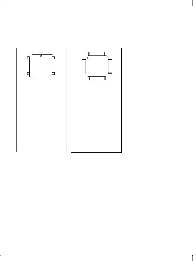
PIN CONFIGURATIONS
|
|
|
P1.0 |
|
|
|
|
|
|
|
|
|
|
|
|
1 |
|
|
|
40 |
|
VDD |
|||
|
|
|
P1.1 |
|
|
|
|
|
|
|
|
|
|
|
|
2 |
|
|
|
39 |
|
P0.0/AD0 |
|||
|
|
|
P1.2 |
|
|
|
|
|
|
|
|
|
|
|
|
3 |
|
|
|
38 |
|
P0.1/AD1 |
|||
|
|
|
|
|
|
|
|
|
|
|
|
|
|
|
|
P1.3 |
4 |
|
|
|
37 |
|
P0.2/AD2 |
||
|
|
|
P1.4 |
|
|
|
|
|
|
|
|
|
|
|
|
|
|
|
|
|
|
|
|
|
|
|
|
|
5 |
|
|
|
36 |
|
P0.3/AD3 |
|||
|
|
|
|
|
|
|
|
|
|
|
|
|
|
|
|
P1.5 |
6 |
|
|
|
35 |
|
P0.4/AD4 |
||
|
|
|
|
|
|
|
|
|
|
|
|
|
SCL/P1.6 |
7 |
|
|
|
34 |
|
P0.5/AD5 |
|||||
|
|
|
|
|
|
|
|
|
|
|
|
|
|
|
|
|
|
|
|
|
|
|
|
|
|
SDA/P1.7 |
8 |
|
|
|
33 |
|
P0.6/AD6 |
|||||
|
|
|
|
|
|
|
|
|
|
|
|
|
|
|
|
RST |
9 |
PLASTIC |
32 |
|
P0.7/AD7 |
||||
|
|
|
|
|
DUAL |
|
|
|
|
|
||
|
|
|
|
|
|
|
|
|
|
|||
RxD/P3.0 |
10 |
IN-LINE |
31 |
|
EA |
|
||||||
|
|
|
|
|
PACKAGE |
|
|
|
|
|
||
TxD/P3.1 |
11 |
|
|
|
30 |
|
ALE |
|||||
|
|
|
|
|
|
|
|
|
|
|
|
|
|
|
|
|
12 |
|
|
|
29 |
|
|
|
|
INT0/P3.2 |
|
|
|
|
PSEN |
|||||||
|
|
|
|
|
|
|
|
|
|
|
|
|
|
|
|
|
13 |
|
|
|
28 |
|
P2.7/A15 |
||
INT1/P3.3 |
|
|
|
|||||||||
|
|
|
|
|
|
|
|
|
|
|
|
|
|
|
T0/P3.4 |
14 |
|
|
|
27 |
|
P2.6/A14 |
|||
|
|
|
|
|
|
|
|
|
|
|
|
|
|
|
T1/P3.5 |
15 |
|
|
|
26 |
|
P2.5/A13 |
|||
|
|
|
|
|
|
|
|
|
|
|
|
|
|
WR/P3.6 |
16 |
|
|
|
25 |
|
P2.4/A12 |
||||
|
|
|
|
|
|
|
|
|
|
|
|
|
|
|
|
|
17 |
|
|
|
24 |
|
P2.3/A11 |
||
RD/P3.7 |
|
|
|
|||||||||
|
|
|
|
|
|
|
|
|
|
|
|
|
|
|
XTAL2 |
18 |
|
|
|
23 |
|
P2.2/A10 |
|||
|
|
|
|
|
|
|
|
|
|
|
|
|
|
|
XTAL1 |
19 |
|
|
|
22 |
|
P2.1/A9 |
|||
|
|
|
|
|
|
|
|
|
|
|
|
|
|
|
|
VSS |
20 |
|
|
|
21 |
|
P2.0/A8 |
||
|
|
|
|
|
|
|
|
|
||||
6 |
1 |
40 |
7 |
|
39 |
|
PLASTIC |
|
|
LEADED |
|
|
CHIP |
|
|
CARRIER |
|
17 |
|
29 |
18 |
|
28 |
44 |
34 |
1 |
33 |
|
PLASTIC |
|
QUAD |
|
FLAT |
|
PACK |
11 |
23 |
12 |
22 |
1997 Dec 05 |
2 |
Phlips Semiconductors |
Product specification |
|
|
|
|
CMOS single-chip 8-bit microcontrollers |
80C652/83C652 |
|
|
|
|
PLASTIC LEADED CHIP CARRIER |
PLASTIC QUAD FLAT PACK |
PIN FUNCTIONS |
PIN FUNCTIONS |
|
6 |
1 |
40 |
|
|
44 |
|
34 |
|
7 |
|
|
39 |
|
1 |
|
33 |
|
|
|
|
|
|
|
||
|
|
PLASTIC |
|
|
|
|
PLASTIC |
|
|
|
|
|
|
|
QUAD |
|
|
|
LEADED CHIP |
|
|
|
|
|||
|
|
|
|
FLAT |
|
|||
|
|
CARRIER |
|
|
|
|
|
|
|
|
|
|
|
|
PACK |
|
|
|
|
|
|
|
|
|
|
|
|
17 |
|
|
29 |
|
11 |
|
23 |
|
|
|
|
|
|
|
||
|
18 |
|
28 |
|
|
12 |
|
22 |
|
|
|
|
|
|
|
||
Pin |
Function |
|
Pin |
Function |
Pin |
Function |
Pin |
Function |
1 |
NC* |
23 |
NC* |
1 |
P1.5 |
23 |
P2.5/A13 |
||||||||||||
2 |
P1.0 |
24 |
P2.0/A8 |
2 |
P1.6/SCL |
24 |
P2.6/A14 |
||||||||||||
3 |
P1.1 |
25 |
P2.1/A9 |
3 |
P1.7/SDA |
25 |
P2.7/A15 |
||||||||||||
4 |
P1.2 |
26 |
P2.2/A10 |
4 |
RST |
26 |
|
|
|
||||||||||
PSEN |
|||||||||||||||||||
5 |
P1.3 |
27 |
P2.3/A11 |
5 |
P3.0/RxD |
27 |
ALE |
||||||||||||
6 |
P1.4 |
28 |
P2.4/A12 |
6 |
VSS4 |
28 |
VSS2 |
||||||||||||
7 |
P1.5 |
29 |
P2.5/A13 |
7 |
P3.1/TxD |
29 |
|
|
|||||||||||
EA/VPP |
|||||||||||||||||||
8 |
P1.6/SCL |
30 |
P2.6/A14 |
|
|
|
|
|
|
|
|
|
|||||||
8 |
P3.2/INT0 |
30 |
P0.7/AD7 |
||||||||||||||||
9 |
P1.7/SDA |
31 |
P2.7/A15 |
||||||||||||||||
|
|
|
|
|
|
|
|
|
|||||||||||
9 |
P3.3/INT1 |
31 |
P0.6/AD6 |
||||||||||||||||
10 |
RST |
32 |
|
|
|
|
|||||||||||||
|
PSEN |
|
10 |
P3.4/T0 |
32 |
P0.5/AD5 |
|||||||||||||
11 |
P3.0/RxD |
33 |
ALE |
11 |
P3.5/T1 |
33 |
P0.4/AD4 |
||||||||||||
12 |
NC* |
34 |
NC* |
||||||||||||||||
|
|
|
|
|
|
|
|
|
|||||||||||
12 |
P3.6/WR |
34 |
P0.3/AD3 |
||||||||||||||||
13 |
P3.1/TxD |
35 |
|
|
|
|
|||||||||||||
|
EA |
|
|
|
|
|
|
|
|
|
|
||||||||
|
|
|
13 |
P3.7/RD |
35 |
P0.2/AD2 |
|||||||||||||
14 |
|
|
|
|
36 |
P0.7/AD7 |
|||||||||||||
P3.2/INT0 |
14 |
XTAL2 |
36 |
P0.1/AD1 |
|||||||||||||||
15 |
P3.3/INT1 |
37 |
P0.6/AD6 |
15 |
XTAL1 |
37 |
P0.0/AD0 |
||||||||||||
16 |
P3.4/T0 |
38 |
P0.5/AD5 |
16 |
VSS1 |
38 |
VDD |
||||||||||||
17 |
P3.5/T1 |
39 |
P0.4/AD4 |
||||||||||||||||
17 |
NC* |
39 |
VSS3 |
||||||||||||||||
18 |
|
|
|
|
40 |
P0.3/AD3 |
|||||||||||||
P3.6/WR |
|
18 |
P2.0/A8 |
40 |
P1.0 |
||||||||||||||
19 |
P3.7/RD |
|
41 |
P0.2/AD2 |
19 |
P2.1/A9 |
41 |
P1.1 |
|||||||||||
20 |
XTAL2 |
42 |
P0.1/AD1 |
20 |
P2.2/A10 |
42 |
P1.2 |
||||||||||||
21 |
XTAL1 |
43 |
P0.0/AD0 |
||||||||||||||||
21 |
P2.3/A11 |
43 |
P1.3 |
||||||||||||||||
22 |
VSS |
44 |
VDD |
||||||||||||||||
22 |
P2.4/A12 |
44 |
P1.4 |
||||||||||||||||
*DO NOT CONNECT |
|
|
|
|
|
*DO NOT CONNECT |
|
|
|
|
|||||||||
|
|
|
|
|
|
|
|
|
|
|
|
|
|
||||||
NOTES TO QFP ONLY:
1.Due to EMC improvements, all VSS pins (6, 16, 28, 39) must be connected to VSS on the 80C652/83C652.
1997 Dec 05 |
3 |
Phlips Semiconductors |
Product specification |
|
|
|
|
CMOS single-chip 8-bit microcontrollers |
80C652/83C652 |
|
|
|
|
ORDER INFORMATION
|
PHILIPS |
|
PHILIPS NORTH AMERICA |
|
|
|||
PART ORDER NUMBER |
|
TEMPERATURE RANGE |
|
|||||
|
PART ORDER NUMBER |
FREQ |
||||||
|
PART MARKING |
|
||||||
|
|
|
|
|
(°C) |
MHz1,2 |
||
|
|
|
|
|
|
|
||
ROMless |
ROM3 |
|
Drawing |
ROMless |
ROM |
EPROM2 |
AND PACKAGE |
|
|
|
|
||||||
|
Number |
|
|
|||||
|
|
|
|
|
|
|
|
|
|
|
|
|
|
|
|
|
|
P80C652EBP |
P83C652EBP/xxx |
|
SOT129-1 |
P80C652EBPN |
P83C652EBPN |
S87C652-4N40 |
0 to +70, |
16 |
|
Plastic Dual In-line Package |
|||||||
|
|
|
|
|
|
|
|
|
|
|
|
|
|
|
|
|
|
P80C652EBA |
P83C652EBA/xxx |
|
SOT187-2 |
P80C652EBAA |
P83C652EBAA |
S87C652-4A44 |
0 to +70, |
16 |
|
Plastic Leaded Chip Carrier |
|||||||
|
|
|
|
|
|
|
|
|
|
|
|
|
|
|
|
|
|
P80C652EBB |
P83C652EBB/xxx |
|
SOT307-2 |
P80C652EBBB |
P83C652EBBB |
S87C652-4B44 |
0 to +70, |
16 |
|
Plastic Quad Flat Pack |
|||||||
|
|
|
|
|
|
|
|
|
|
|
|
|
|
|
|
|
|
P80C652EFP |
P83C652EFP/xxx |
|
SOT129-1 |
P80C652EFPN |
P83C652EFPN |
S87C652-5N40 |
±40 to +85, |
16 |
|
Plastic Dual In-line Package |
|||||||
|
|
|
|
|
|
|
|
|
|
|
|
|
|
|
|
|
|
P80C652EFA |
P83C652EFA/xxx |
|
SOT187-2 |
P80C652EFAA |
P83C652EFAA |
S87C652-5A44 |
±40 to +85, |
16 |
|
Plastic Leaded Chip Carrier |
|||||||
|
|
|
|
|
|
|
|
|
|
|
|
|
|
|
|
|
|
P80C652EFB |
P83C652EFB/xxx |
|
SOT307-2 |
P80C652EFBB |
P83C652EFBB |
S87C652-5B44 |
±40 to +85, |
16 |
|
Plastic Quad Flat Pack |
|||||||
|
|
|
|
|
|
|
|
|
|
|
|
|
|
|
|
|
|
P80C652EHP |
P83C652EHP/xxx |
|
SOT129-1 |
P80C652EHPN |
P83C652EHPN |
|
±40 to +125, |
16 |
|
|
Plastic Dual In-line Package |
||||||
|
|
|
|
|
|
|
|
|
|
|
|
|
|
|
|
|
|
P80C652EHA |
P83C652EHA/xxx |
|
SOT187-2 |
P80C652EHAA |
P83C652EHAA |
|
±40 to +125, |
16 |
|
|
Plastic Leaded Chip Carrier |
||||||
|
|
|
|
|
|
|
|
|
|
|
|
|
|
|
|
|
|
P80C652EHB |
P83C652EHB/xxx |
|
SOT307-2 |
P80C652EHBB |
P83C652EHBB |
|
±40 to +125, |
16 |
|
|
Plastic Quad Flat Pack |
||||||
|
|
|
|
|
|
|
|
|
|
|
|
|
|
|
|
|
|
P80C652IBP |
P83C652IBP/xxx |
|
SOT129-1 |
P80C652IBPN |
P83C652IBPN |
|
0 to +70, |
24 |
|
|
Plastic Dual In-line Package |
||||||
|
|
|
|
|
|
|
|
|
|
|
|
|
|
|
|
|
|
P80C652IBA |
P83C652IBA/xxx |
|
SOT187-2 |
P80C652IBAA |
P83C652IBAA |
|
0 to +70, |
24 |
|
|
Plastic Leaded Chip Carrier |
||||||
|
|
|
|
|
|
|
|
|
|
|
|
|
|
|
|
|
|
P80C652IBB |
P83C652IBB/xxx |
|
SOT307-2 |
P80C652IBBB |
P83C652IBBB |
|
0 to +70, |
24 |
|
|
Plastic Quad Flat Pack |
||||||
|
|
|
|
|
|
|
|
|
|
|
|
|
|
|
|
|
|
P80C652IFP |
P83C652IFP/xxx |
|
SOT129-1 |
P80C652IFPN |
P83C652IFPN |
|
±40 to +85, |
24 |
|
|
Plastic Dual In-line Package |
||||||
|
|
|
|
|
|
|
|
|
|
|
|
|
|
|
|
|
|
P80C652IFA |
P83C652IFA/xxx |
|
SOT187-2 |
P80C652IFAA |
P83C652IFAA |
|
±40 to +85, |
24 |
|
|
Plastic Leaded Chip Carrier |
||||||
|
|
|
|
|
|
|
|
|
|
|
|
|
|
|
|
|
|
P80C652IFB |
P83C652IFB/xxx |
|
SOT307-2 |
P80C652IFBB |
P83C652IFBB |
|
±40 to +85, |
24 |
|
|
Plastic Quad Flat Pack |
||||||
|
|
|
|
|
|
|
|
|
|
|
|
|
|
|
|
|
|
NOTES:
1.80C652 and 83C652 frequency range is 3.5MHz±16MHz or 3.5MHz±24MHz.
2.For specification of the EPROM version, see the 87C652 data sheet.
3.xxx denotes the ROM code number.
1997 Dec 05 |
4 |
Phlips Semiconductors |
Product specification |
|
|
|
|
CMOS single-chip 8-bit microcontrollers |
80C652/83C652 |
|
|
|
|
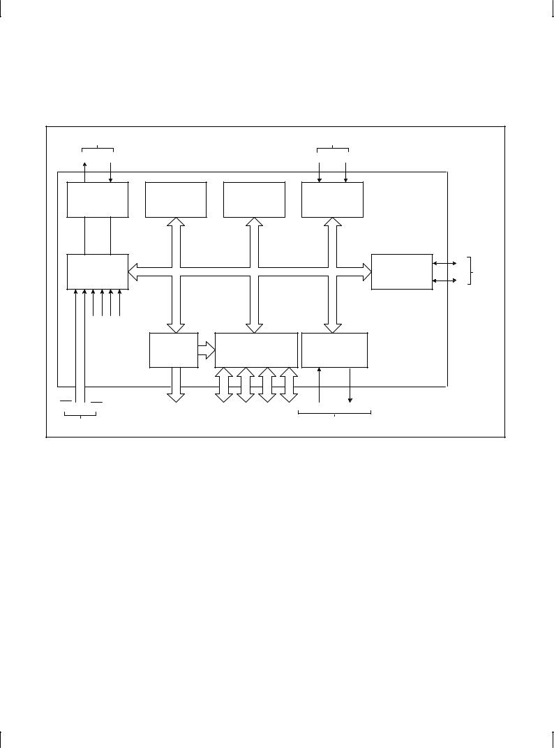
BLOCK DIAGRAM
FREQUENCY |
|
|
COUNTERS |
|
||
REFERENCE |
|
|
|
|||
XTAL2 |
XTAL1 |
|
|
T0 |
T1 |
|
OSCILLATOR |
PROGRAM |
DATA |
TWO 16-BIT |
|
||
AND |
MEMORY |
MEMORY |
TIMER/EVENT |
|
||
TIMING |
(8K x 8 ROM) |
(256 x 8 RAM) |
COUNTERS |
|
||
|
|
|
|
|
SDA |
SHARED |
|
CPU |
|
|
|
I2C SERIAL I/O |
WITH |
|
|
|
|
|
SCL |
PORT 1 |
|
|
|
|
|
|
|
|
INTERNAL |
|
|
|
|
|
INTERRUPTS |
|
|
|
|
|
|
|
|
64K BYTE BUS |
PROGRAMMABLE I/O |
PROG SERIAL PORT |
|
|
|
|
EXPANSION |
FULL DUPLEX UART |
|
||
|
|
CONTRTOL |
|
SYNCHRONOUS SHIFT |
|
|
INT0 |
INT1 |
CONTROL |
PARALLEL PORTS, |
SERIAL IN |
SERIAL OUT |
|
|
|
|||||
|
|
|
ADDRESS/DATA BUS |
|
|
|
EXTERNAL |
|
AND I/O PINS |
SHARED WITH |
|
||
|
|
|
||||
|
|
PORT 3 |
|
|||
INTERRUPTS |
|
|
|
|||
|
|
|
|
|
||
1997 Dec 05 |
5 |

Phlips Semiconductors |
Product specification |
|
|
|
|
CMOS single-chip 8-bit microcontrollers |
80C652/83C652 |
|
|
|
|
PIN DESCRIPTIONS
|
|
|
|
PIN NUMBER |
|
|
|
|
|
|
|
|
|
||
|
|
|
|
|
|
|
|
|
|
|
|
|
|
|
|
|
MNEMONIC |
DIP |
PLCC |
QFP |
TYPE |
NAME AND FUNCTION |
|||||||||
|
|
|
|
|
|
|
|
|
|
|
|
|
|
|
|
|
VSS |
20 |
22 |
6, 16, |
I |
Ground: 0V reference. With the QFP package all VSS pins (VSS1 to VSS4) must be |
|||||||||
|
|
|
|
|
|
28, 39 |
|
connected. |
|||||||
|
VDD |
40 |
44 |
38 |
I |
Power Supply: This is the power supply voltage for normal, idle, and power-down |
|||||||||
|
|
|
|
|
|
|
|
operation. |
|||||||
|
P0.0±0.7 |
39±32 |
43±36 |
37±30 |
I/O |
Port 0: Port 0 is an open-drain, bidirectional I/O port. Port 0 pins that have 1s written to |
|||||||||
|
|
|
|
|
|
|
|
them float and can be used as high-impedance inputs. Port 0 is also the multiplexed |
|||||||
|
|
|
|
|
|
|
|
low-order address and data bus during accesses to external program and data memory. In |
|||||||
|
|
|
|
|
|
|
|
this application, it uses strong internal pull-ups when emitting 1s. |
|||||||
|
P1.0±P1.7 |
1±8 |
2±9 |
40±44, |
I/O |
Port 1: Port 1 is an 8-bit bidirectional I/O port with internal pull-ups, except P1.6 and P1.7 |
|||||||||
|
|
|
|
|
|
1±3 |
|
which are open drain. Port 1 pins that have 1s written to them are pulled high by the |
|||||||
|
|
|
|
|
|
|
|
internal pull-ups and can be used as inputs. As inputs, port 1 pins that are externally pulled |
|||||||
|
|
|
|
|
|
|
|
low will source current because of the internal pull-ups. (See DC Electrical Characteristics: |
|||||||
|
|
|
|
|
|
|
|
IIL). Alternate functions include: |
|||||||
|
P1.6 |
7 |
8 |
2 |
I/O |
|
SCL: I2C-bus serial port clock line. |
||||||||
|
P1.7 |
8 |
9 |
3 |
I/O |
|
SDA: I2C-bus serial port data line. |
||||||||
|
P2.0±P2.7 |
21±28 |
24±31 |
18±25 |
I/O |
Port 2: Port 2 is an 8-bit bidirectional I/O port with internal pull-ups. Port 2 pins that have 1s |
|||||||||
|
|
|
|
|
|
|
|
written to them are pulled high by the internal pull-ups and can be used as inputs. As |
|||||||
|
|
|
|
|
|
|
|
inputs, port 2 pins that are externally being pulled low will source current because of the |
|||||||
|
|
|
|
|
|
|
|
internal pull-ups. (See DC Electrical Characteristics: IIL). Port 2 emits the high-order |
|||||||
|
|
|
|
|
|
|
|
address byte during fetches from external program memory and during accesses to |
|||||||
|
|
|
|
|
|
|
|
external data memory that use 16-bit addresses (MOVX @DPTR). In this application, it |
|||||||
|
|
|
|
|
|
|
|
uses strong internal pull-ups when emitting 1s. During accesses to external data memory |
|||||||
|
|
|
|
|
|
|
|
that use 8-bit addresses (MOV @Ri), port 2 emits the contents of the P2 special function |
|||||||
|
|
|
|
|
|
|
|
register. |
|||||||
|
P3.0±P3.7 |
10±17 |
11, |
5, |
I/O |
Port 3: Port 3 is an 8-bit bidirectional I/O port with internal pull-ups. Port 3 pins that have 1s |
|||||||||
|
|
|
|
|
13±19 |
7±13 |
|
written to them are pulled high by the internal pull-ups and can be used as inputs. As |
|||||||
|
|
|
|
|
|
|
|
inputs, port 3 pins that are externally being pulled low will source current because of the |
|||||||
|
|
|
|
|
|
|
|
pull-ups. (See DC Electrical Characteristics: IIL). Port 3 also serves the special features of |
|||||||
|
|
|
|
|
|
|
|
the 80C51 family, as listed below: |
|||||||
|
|
|
|
10 |
11 |
5 |
I |
|
RxD (P3.0): Serial input port |
||||||
|
|
|
|
11 |
13 |
7 |
O |
|
TxD (P3.1): Serial output port |
||||||
|
|
|
|
12 |
14 |
8 |
I |
|
|
|
|
|
(P3.2): External interrupt |
||
|
|
|
|
|
INT0 |
||||||||||
|
|
|
|
13 |
15 |
9 |
I |
|
|
|
|
(P3.3): External interrupt |
|||
|
|
|
|
|
INT1 |
||||||||||
|
|
|
|
14 |
16 |
10 |
I |
|
T0 (P3.4): Timer 0 external input |
||||||
|
|
|
|
15 |
17 |
11 |
I |
|
T1 (P3.5): Timer 1 external input |
||||||
|
|
|
|
16 |
18 |
12 |
O |
|
|
|
(P3.6): External data memory write strobe |
||||
|
|
|
|
|
WR |
||||||||||
|
|
|
|
17 |
19 |
13 |
O |
|
|
(P3.7): External data memory read strobe |
|||||
|
|
|
|
|
RD |
||||||||||
|
RST |
9 |
10 |
4 |
I |
Reset: A high on this pin for two machine cycles while the oscillator is running, resets the |
|||||||||
|
|
|
|
|
|
|
|
device. An internal diffused resistor to VSS permits a power-on reset using only an external |
|||||||
|
|
|
|
|
|
|
|
capacitor to VDD. |
|||||||
|
ALE |
30 |
33 |
27 |
I/O |
Address Latch Enable: Output pulse for latching the low byte of the address during an |
|||||||||
|
|
|
|
|
|
|
|
access to external memory. In normal operation, ALE is emitted at a constant rate of 1/6 |
|||||||
|
|
|
|
|
|
|
|
the oscillator frequency. Note that one ALE pulse is skipped during each access to external |
|||||||
|
|
|
|
|
|
|
|
data memory. |
|||||||
|
|
|
|
29 |
32 |
26 |
O |
Program Store Enable: Read strobe to external program memory via Port 0 and Port 2. It |
|||||||
|
PSEN |
||||||||||||||
|
|
|
|
|
|
|
|
is activated twice each machine cycle during fetches from the external program memory. |
|||||||
|
|
|
|
|
|
|
|
When executing out of external program memory two activations of PSEN are skipped |
|||||||
|
|
|
|
|
|
|
|
during each access to external data memory. PSEN is not activated (remains HIGH) during |
|||||||
|
|
|
|
|
|
|
|
no fetches from external program memory. PSEN can sink/source 8 LSTTL inputs and can |
|||||||
|
|
|
|
|
|
|
|
drive CMOS inputs without external pull±ups. |
|||||||
|
|
|
31 |
35 |
29 |
I |
External Access: If during a RESET, |
|
is held at TTL, level HIGH, the CPU executes out |
||||||
|
EA |
EA |
|||||||||||||
|
|
|
|
|
|
|
|
of the internal program memory ROM provided the Program Counter is less than 8192. If |
|||||||
|
|
|
|
|
|
|
|
during a RESET, EA is held a TTL LOW level, the CPU executes out of external program |
|||||||
|
|
|
|
|
|
|
|
memory. EA is not allowed to float. |
|||||||
|
XTAL1 |
19 |
21 |
15 |
I |
Crystal 1: Input to the inverting oscillator amplifier and input to the internal clock generator |
|||||||||
|
|
|
|
|
|
|
|
circuits. |
|||||||
|
XTAL2 |
18 |
20 |
14 |
O |
Crystal 2: Output from the inverting oscillator amplifier. |
|||||||||
NOTE: |
|
|
|
To avoid ªlatch-upº effect at power-on, the voltage on any pin at any time must not be higher than V |
+ 0.5V or V |
SS |
± 0.5V, respectively. |
DD |
|
|
1997 Dec 05 |
6 |
Phlips Semiconductors |
Product specification |
|
|
|
|
CMOS single-chip 8-bit microcontrollers |
80C652/83C652 |
|
|
|
|
Table 1. |
8XC652/654 Special Function Registers |
|
|
|
|
|
|
|
|
|
|
|
|
|
|
|||||||||
SYMBOL |
DESCRIPTION |
DIRECT |
|
BIT ADDRESS, SYMBOL, OR ALTERNATIVE PORT FUNCTION |
|
RESET |
||||||||||||||||||
ADDRESS |
MSB |
|
|
|
|
|
|
|
|
|
|
|
|
|
|
|
|
|
LSB |
VALUE |
||||
|
|
|
|
|
|
|
|
|
|
|
|
|
|
|
|
|
|
|
||||||
|
|
|
|
|
|
|
|
|
|
|
|
|
|
|
|
|
|
|
|
|
|
|
|
|
ACC* |
Accumulator |
E0H |
|
E7 |
|
E6 |
E5 |
E4 |
|
E3 |
|
E2 |
E1 |
E0 |
00H |
|||||||||
B* |
B register |
F0H |
|
F7 |
|
F6 |
F5 |
F4 |
|
F3 |
|
F2 |
F1 |
F0 |
00H |
|||||||||
DPTR: |
Data pointer |
|
|
|
|
|
|
|
|
|
|
|
|
|
|
|
|
|
|
|
|
|
|
|
|
(2 bytes) |
|
|
|
|
|
|
|
|
|
|
|
|
|
|
|
|
|
|
|
|
|
|
|
DPH |
Data pointer high |
83H |
|
|
|
|
|
|
|
|
|
|
|
|
|
|
|
|
|
|
|
|
|
00H |
DPL |
Data pointer low |
82H |
|
|
|
|
|
|
|
|
|
|
|
|
|
|
|
|
|
|
|
|
|
00H |
|
|
|
|
AF |
|
AE |
AD |
AC |
|
AB |
|
AA |
A9 |
A8 |
|
|||||||||
|
|
|
|
|
|
|
|
|
|
|
|
|
|
|
|
|
|
|
|
|
|
|
|
|
IE*# |
Interrupt enable |
A8H |
|
EA |
|
|
|
|
|
ES1 |
ES0 |
|
ET1 |
|
EX1 |
ET0 |
|
EX0 |
0x000000B |
|||||
|
|
|
|
|
|
|
|
|
|
|
|
|
|
|
|
|
|
|
|
|
|
|
|
|
|
|
|
|
BF |
|
BE |
BD |
BC |
|
BB |
|
BA |
B9 |
B8 |
|
|||||||||
|
|
|
|
|
|
|
|
|
|
|
|
|
|
|
|
|
|
|
|
|
|
|
|
|
IP*# |
Interrupt priority |
B8H |
± |
|
|
|
|
|
|
PS1 |
PS0 |
|
PT1 |
|
PX1 |
PT0 |
|
PX0 |
xx000000B |
|||||
|
|
|
|
|
|
|
|
|
|
|
|
|
|
|
|
|
|
|
|
|
|
|
|
|
|
|
|
87 |
|
86 |
|
|
85 |
84 |
83 |
|
82 |
|
|
81 |
|
80 |
|
||||||
|
|
|
|
|
|
|
|
|
|
|
|
|
|
|
|
|
|
|
|
|
|
|
|
|
P0* |
Port 0 |
80H |
AD7 |
AD6 |
AD5 |
AD4 |
|
AD3 |
|
AD2 |
AD1 |
|
AD0 |
FFH |
||||||||||
|
|
|
|
|
|
|
|
|
|
|
|
|
|
|
|
|
|
|
|
|
|
|
|
|
|
|
|
97 |
|
96 |
|
|
95 |
94 |
93 |
|
92 |
|
|
91 |
|
90 |
|
||||||
|
|
|
|
|
|
|
|
|
|
|
|
|
|
|
|
|
|
|
|
|
|
|
|
|
P1*# |
Port 1 |
90H |
SDA |
SCL |
|
|
|
|
|
|
|
|
|
|
|
|
|
FFH |
||||||
|
|
|
|
|
|
|
|
|
|
|
|
|
|
|
|
|
|
|
|
|
|
|
|
|
|
|
|
|
A7 |
|
A6 |
A5 |
A4 |
|
A3 |
|
A2 |
A1 |
A0 |
|
|||||||||
|
|
|
|
|
|
|
|
|
|
|
|
|
|
|
|
|
|
|
|
|
|
|
|
|
P2* |
Port 2 |
A0H |
A15 |
A14 |
A13 |
A12 |
|
A11 |
|
A10 |
A9 |
|
A8 |
FFH |
||||||||||
|
|
|
|
|
|
|
|
|
|
|
|
|
|
|
|
|
|
|
|
|
|
|
|
|
|
|
|
|
B7 |
|
B6 |
B5 |
B4 |
|
B3 |
|
B2 |
B1 |
B0 |
|
|||||||||
|
|
|
|
|
|
|
|
|
|
|
|
|
|
|
|
|
|
|
|
|
|
|
|
|
P3* |
Port 3 |
B0H |
|
|
|
|
|
|
|
|
T1 |
T0 |
|
|
|
|
|
|
|
|
TXD |
|
RXD |
FFH |
RD |
WR |
INT1 |
INT0 |
|||||||||||||||||||||
PCON |
Power control |
87H |
SMOD |
± |
|
|
± |
± |
|
GF1 |
|
GF0 |
PD |
|
IDL |
0xxx0000B |
||||||||
|
|
|
|
|
|
|
|
|
|
|
|
|
|
|
|
|
|
|
|
|
|
|
||
|
|
|
|
9F |
|
9E |
9D |
9C |
|
9B |
|
9A |
99 |
|
98 |
|
||||||||
|
|
|
|
|
|
|
|
|
|
|
|
|
|
|
|
|
|
|||||||
S0CON*# |
Serial 0 port control |
98H |
SM0 |
SM1 |
SM2 |
REN |
|
TB8 |
|
RB8 |
TI |
|
RI |
00H |
||||||||||
S0BUF# |
Serial 0 data buffer |
99H |
|
|
|
|
|
|
|
|
|
|
|
|
|
|
|
|
|
|
|
|
|
xxxxxxxxB |
|
|
|
|
|
|
|
|
|
|
|
|
|
|
|
|
|
|
|
|
|
||||
|
|
|
|
D7 |
|
D6 |
D5 |
D4 |
|
D3 |
|
D2 |
D1 |
D0 |
|
|||||||||
|
|
|
|
|
|
|
|
|
|
|
|
|
|
|
|
|
|
|
|
|||||
PSW* |
Program status word |
D0H |
|
CY |
|
AC |
F0 |
RS1 |
|
RS0 |
|
OV |
F1 |
|
P |
00H |
||||||||
S1DAT# |
Serial 1 data |
DAH |
|
|
|
|
|
|
|
|
|
|
|
|
|
|
|
|
|
|
|
|
|
00H |
|
|
|
|
|
|
|
|
|
|
|
|
|
|
|
|
|
|
|
|
|
||||
SP |
Stack pointer |
81H |
|
|
|
|
|
|
|
|
|
|
|
|
|
|
|
|
|
|
|
|
|
07H |
|
|
|
|
|
|
|
|
|
|
|
|
|
||||||||||||
S1ADR# |
Serial 1 address |
DBH |
|
SLAVE ADDRESS |
|
|
GC |
00H |
||||||||||||||||
|
|
|
|
|
|
|
|
|
|
|
|
|
|
|
|
|
|
|
||||||
|
|
|
|
|
|
|
|
|
|
|
|
|
|
|
|
|
|
|
||||||
S1STA# |
Serial 1 status |
D9H |
SC4 |
SC3 |
SC2 |
SC1 |
|
SC0 |
0 |
|
|
0 |
|
0 |
F8H |
|||||||||
|
|
|
|
|
|
|
|
|
|
|
|
|
|
|
|
|
|
|
|
|
||||
|
|
|
|
DF |
|
DE |
DD |
DC |
|
DB |
|
DA |
D9 |
D8 |
|
|||||||||
|
|
|
|
|
|
|
|
|
|
|
|
|
|
|
|
|
|
|||||||
S1CON*# |
Serial 1 control |
D8H |
CR2 |
ENS1 |
STA |
STO |
|
SI |
|
AA |
CR1 |
|
CR0 |
00000000B |
||||||||||
|
|
|
|
|
|
|
|
|
|
|
|
|
|
|
|
|
|
|
|
|
||||
|
|
|
|
8F |
|
8E |
8D |
8C |
|
8B |
|
8A |
89 |
|
88 |
|
||||||||
|
|
|
|
|
|
|
|
|
|
|
|
|
|
|
|
|
|
|||||||
TCON* |
Timer control |
88H |
TF1 |
TR1 |
TF0 |
TR0 |
|
IE1 |
|
IT1 |
IE0 |
|
IT0 |
00H |
||||||||||
TH1 |
Timer high 1 |
8DH |
|
|
|
|
|
|
|
|
|
|
|
|
|
|
|
|
|
|
|
|
|
00H |
|
|
|
|
|
|
|
|
|
|
|
|
|
|
|
|
|
|
|
|
|
||||
TH0 |
Timer high 0 |
8CH |
|
|
|
|
|
|
|
|
|
|
|
|
|
|
|
|
|
|
|
|
|
00H |
TL1 |
Timer low 1 |
8BH |
|
|
|
|
|
|
|
|
|
|
|
|
|
|
|
|
|
|
|
|
|
00H |
TL0 |
Timer low 0 |
8AH |
|
|
|
|
|
|
|
|
|
|
|
|
|
|
|
|
|
|
|
|
|
00H |
|
|
|
|
|
|
|
|
|
|
|
|
|
|
|
|
|
|
|||||||
TMOD |
Timer mode |
89H |
GATE |
|
|
|
|
M1 |
M0 |
GATE |
|
|
|
|
M1 |
|
M0 |
00H |
||||||
|
C/T |
|
|
C/T |
|
|||||||||||||||||||
*SFRs are bit addressable.
# SFRs are modified from or added to the 80C51 SFRs.
1997 Dec 05 |
7 |
 Loading...