


Philips PCA80C31BH3-16P, PCA80C51BH-3P, PCA80C51BH-3WP, PCB80C31-2A, PCB80C31-2N Datasheet
...INTEGRATED CIRCUITS
80C31/80C51/87C51
CMOS single-chip 8-bit microcontrollers
Product specification |
1996 Aug 16 |
IC20 Data Handbook

Philips Semiconductors |
Product specification |
|
|
|
|
CMOS single-chip 8-bit microcontrollers |
80C31/80C51/87C51 |
|
|
|
|
DESCRIPTION
The Philips 80C31/80C51/87C51 is a high-performance microcontroller fabricated with Philips high-density CMOS technology. The CMOS 8XC51 is functionally compatible with the NMOS 8031/8051 microcontrollers. The Philips CMOS technology combines the high speed and density characteristics of HMOS with the low power attributes of CMOS. Philips epitaxial substrate minimizes latch-up sensitivity.
The 8XC51 contains a 4k × 8 ROM (80C51) EPROM (87C51), a 128 × 8 RAM, 32 I/O lines, two 16-bit counter/timers, a five-source, two-priority level nested interrupt structure, a serial I/O port for either multi-processor communications, I/O expansion or full duplex UART, and on-chip oscillator and clock circuits.
In addition, the device has two software selectable modes of power reductionÐidle mode and power-down mode. The idle mode freezes the CPU while allowing the RAM, timers, serial port, and interrupt system to continue functioning. The power-down mode saves the RAM contents but freezes the oscillator, causing all other chip functions to be inoperative.
FEATURES
•8031/8051 compatible
±4k × 8 ROM (80C51)
±4k × 8 EPROM (87C51)
±ROMless (80C31)
±128 × 8 RAM
±Two 16-bit counter/timers
±Full duplex serial channel
±Boolean processor
•Memory addressing capability
± 64k ROM and 64k RAM
•Power control modes:
±Idle mode
±Power-down mode
•CMOS and TTL compatible
•Five speed ranges at VCC = 5V
±12MHz
±16MHz
±24MHz
±33MHz
•Five package styles
•Extended temperature ranges
•OTP package available
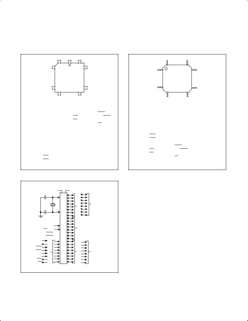
PIN CONFIGURATIONS
|
P1.0 |
1 |
|
40 |
VCC |
||||
|
P1.1 |
2 |
|
39 |
P0.0/AD0 |
||||
|
P1.2 |
3 |
|
38 |
P0.1/AD1 |
||||
|
P1.3 |
4 |
|
37 |
P0.2/AD2 |
||||
|
P1.4 |
5 |
|
36 |
P0.3/AD3 |
||||
|
P1.5 |
6 |
|
35 |
P0.4/AD4 |
||||
|
P1.6 |
7 |
|
34 |
P0.5/AD5 |
||||
|
P1.7 |
8 |
|
33 |
P0.6/AD6 |
||||
|
RST |
9 |
CERAMIC |
32 |
P0.7/AD7 |
||||
RxD/P3.0 10 |
AND |
31 |
|
|
|
|
|
||
PLASTIC |
|
EA/VPP |
|||||||
TxD/P3.1 11 |
DUAL |
30 |
|
|
|
|
|
||
IN-LINE |
ALE/PROG |
||||||||
|
|
|
PACKAGE |
|
|
|
|
|
|
|
|
|
|
|
|
|
|
|
|
INT0/P3.2 12 |
|
29 |
PSEN |
|
INT1/P3.3 13 |
|
28 |
P2.7/A15 |
|
T0/P3.4 |
14 |
|
27 |
P2.6/A14 |
T1/P3.5 |
15 |
|
26 |
P2.5/A13 |
WR/P3.6 16 |
|
25 |
P2.4/A12 |
|
RD/P3.7 17 |
|
24 |
P2.3/A11 |
|
XTAL2 |
18 |
|
23 |
P2.2/A10 |
XTAL1 |
19 |
|
22 |
P2.1/A9 |
VSS 20 |
|
21 |
P2.0/A8 |
|
|
6 |
1 |
40 |
|
7 |
|
|
|
39 |
|
|
CERAMIC |
|
|
|
|
AND |
|
|
|
|
PLASTIC |
|
|
|
|
LEAD |
|
|
|
|
CHIP |
|
|
17 |
|
CARRIER |
|
29 |
|
|
|
||
|
18 |
|
28 |
|
|
44 |
|
34 |
|
1 |
|
|
|
33 |
PLASTIC
QUAD
FLAT
PACK
11 |
|
|
|
|
23 |
|||||
|
|
|
|
|||||||
|
|
|||||||||
|
|
|
|
|
|
|
|
|
|
|
|
|
|
|
|
|
|
|
|
|
|
12 |
22 |
SU00001
SEE PAGE 3 FOR QFP AND LCC PIN FUNCTIONS.
1996 Aug 16 |
2 |
853±0169 17187 |
Philips Semiconductors |
Product specification |
|
|
|
|
CMOS single-chip 8-bit microcontrollers |
80C31/80C51/87C51 |
|
|
|
|
CERAMIC AND PLASTIC LEADED CHIP CARRIER |
PLASTIC QUAD FLAT PACK |
PIN FUNCTIONS |
PIN FUNCTIONS |
|
|
6 |
1 |
40 |
|
|
|
44 |
34 |
|
|
|
7 |
|
|
39 |
|
|
1 |
|
|
33 |
|
|
|
|
|
|
|
|
|
|
|
||
|
|
|
LCC |
|
|
|
|
|
PQFP |
|
|
|
|
|
|
|
|
|
|
|
|
|
|
|
17 |
|
|
29 |
|
|
11 |
|
|
23 |
|
|
|
18 |
|
28 |
|
|
|
12 |
22 |
|
|
|
|
|
|
|
|
|
|
|
|
||
Pin |
Function |
Pin |
Function |
Pin |
Function |
Pin |
Function |
Pin |
Function |
Pin |
Function |
1 |
NC* |
16 |
P3.4/T0 |
31 |
P2.7/A15 |
1 |
P1.5 |
16 |
VSS |
31 |
P0.6/AD6 |
2 |
P1.0 |
17 |
P3.5/T1 |
32 |
PSEN |
2 |
P1.6 |
17 |
NC* |
32 |
P0.5/AD5 |
3 |
P1.1 |
18 |
P3.6/WR |
33 |
ALE/PROG |
3 |
P1.7 |
18 |
P2.0/A8 |
33 |
P0.4/AD4 |
4 |
P1.2 |
19 |
P3.7/RD |
34 |
NC* |
4 |
RST |
19 |
P2.1/A9 |
34 |
P0.3/AD3 |
5 |
P1.3 |
20 |
XTAL2 |
35 |
EA/VPP |
5 |
P3.0/RxD |
20 |
P2.2/A10 |
35 |
P0.2/AD2 |
6 |
P1.4 |
21 |
XTAL1 |
36 |
P0.7/AD7 |
6 |
NC* |
21 |
P2.3/A11 |
36 |
P0.1/AD1 |
7 |
P1.5 |
22 |
VSS |
37 |
P0.6/AD6 |
7 |
P3.1/TxD |
22 |
P2.4/A12 |
37 |
P0.0/AD0 |
8 |
P1.6 |
23 |
NC* |
38 |
P0.5/AD5 |
8 |
P3.2/INT0 |
23 |
P2.5/A13 |
38 |
VCC |
9 |
P1.7 |
24 |
P2.0/A8 |
39 |
P0.4/AD4 |
9 |
P3.3/INT1 |
24 |
P2.6/A14 |
39 |
NC* |
10 |
RST |
25 |
P2.1/A9 |
40 |
P0.3/AD3 |
10 |
P3.4/T0 |
25 |
P2.7/A15 |
40 |
P1.0 |
11 |
P3.0/RxD |
26 |
P2.2/A10 |
41 |
P0.2/AD2 |
11 |
P3.5/T1 |
26 |
PSEN |
41 |
P1.1 |
12 |
NC* |
27 |
P2.3/A11 |
42 |
P0.1/AD1 |
12 |
P3.6/WR |
27 |
ALE/PROG |
42 |
P1.2 |
13 |
P3.1/TxD |
28 |
P2.4/A12 |
43 |
P0.0/AD0 |
13 |
P3.7/RD |
28 |
NC* |
43 |
P.13 |
14 |
P3.2/INT0 |
29 |
P2.5/A13 |
44 |
VCC |
14 |
XTAL2 |
29 |
EA/VPP |
44 |
P1.4 |
15 |
P3.3/INT1 |
30 |
P2.6/A14 |
|
|
15 |
XTAL1 |
30 |
P0.7/AD7 |
|
|
* DO NOT CONNECT |
SU00002 |
* DO NOT CONNECT |
SU00003 |
|
|
LOGIC SYMBOL
SECONDARY FUNCTIONS
VCC VSS
XTAL1
XTAL2
RST
EA/VPP
PSEN 
ALE/PROG

RxD |
|
|
TxD |
|
|
INT0 |
3 |
|
INT1 |
||
PORT |
||
T0 |
||
T1 |
|
|
WR |
|
|
RD |
|
0 |
ADDRESS AND |
PORT |
DATA BUS |
|
|
PORT 1 |
|
2 |
|
PORT |
ADDRESS BUS |
|
SU00004
1996 Aug 16 |
3 |

Philips Semiconductors |
Product specification |
|
|
|
|
CMOS single-chip 8-bit microcontrollers |
80C31/80C51/87C51 |
|
|
|
|
ORDERING INFORMATION
|
|
|
|
PHILIPS NORTH AMERICA |
|
|
|
|
|
|
|
|
|
|
DRAWING |
|
|
DRAWING |
TEMPERATURE RANGE oC |
Freq |
EPROM |
NUMBER |
ROMless |
ROM |
NUMBER |
AND PACKAGE1 |
MHz |
SC87C51CCF40 |
0590B |
|
|
|
0 to +70, Ceramic Dual In-line Package, UV |
3.5 to 12 |
|
|
|
|
|
|
|
SC87C51CCK44 |
1472A |
|
|
|
0 to +70, Ceramic Leaded Chip Carrier, UV |
3.5 to 12 |
|
|
|
|
|
|
|
SC87C51CCN40 |
SOT129-1 |
SC80C31BCCN40 |
SC80C51BCCN40 |
SOT129-1 |
0 to +70, Plastic Dual In-line Package, OTP |
3.5 to 12 |
|
|
|
|
|
|
|
SC87C51CCA44 |
SOT187-2 |
SC80C31BCCA44 |
SC80C51BCCA44 |
SOT187-2 |
0 to +70, Plastic Leaded Chip Carrier, OTP |
3.5 to 12 |
|
|
|
|
|
|
|
SC87C51CCB44 |
SOT307-2 |
SC80C31BCCB44 |
SC80C51BCCB44 |
SOT307-2 |
0 to +70, Plastic Quad Flat Pack, OTP |
3.5 to 12 |
|
|
|
|
|
|
|
SC87C51ACF40 |
0590B |
|
|
|
±40 to +85, Ceramic Dual In-line Package, UV |
3.5 to 12 |
|
|
|
|
|
|
|
SC87C51ACN40 |
SOT129-1 |
SC80C31BACN40 |
SC80C51BACN40 |
SOT129-1 |
±40 to +85, Plastic Dual In-line Package, OTP |
3.5 to 12 |
|
|
|
|
|
|
|
SC87C51ACA44 |
SOT187-2 |
SC80C31BACA44 |
SC80C51BACA44 |
SOT187-2 |
±40 to +85, Plastic Leaded Chip Carrier, OTP |
3.5 to 12 |
|
|
|
|
|
|
|
SC87C51ACB44 |
SOT307-2 |
SC80C31BACB44 |
SC80C51BACB44 |
SOT307-2 |
±40 to +85, Plastic Quad Flat Pack, OTP |
3.5 to 12 |
|
|
|
|
|
|
|
SC87C51CGF40 |
0590B |
|
|
|
0 to +70, Ceramic Dual In-line Package, UV |
3.5 to 16 |
|
|
|
|
|
|
|
SC87C51CGK44 |
1472A |
|
|
|
0 to +70, Ceramic Leaded Chip Carrier, UV |
3.5 to 16 |
|
|
|
|
|
|
|
SC87C51CGN40 |
SOT129-1 |
SC80C31BCGN40 |
SC80C51BCGN40 |
SOT129-1 |
0 to +70, Plastic Dual In-line Package, OTP |
3.5 to 16 |
|
|
|
|
|
|
|
SC87C51CGA44 |
SOT187-2 |
SC80C31BCGA44 |
SC80C51BCGA44 |
SOT187-2 |
0 to +70, Plastic Leaded Chip Carrier, OTP |
3.5 to 16 |
|
|
|
|
|
|
|
SC87C51CGB44 |
SOT307-2 |
SC80C31BCGB44 |
SC80C51BCGB44 |
SOT307-2 |
0 to +70, Plastic Quad Flat Pack, OTP |
3.5 to 16 |
|
|
|
|
|
|
|
SC87C51AGF40 |
0590B |
|
|
|
±40 to +85, Ceramic Dual In-line Package, UV |
3.5 to 16 |
|
|
|
|
|
|
|
SC87C51AGN40 |
SOT129-1 |
SC80C31BAGN40 |
SC80C51BAGN40 |
SOT129-1 |
±40 to +85, Plastic Dual In-line Package, OTP |
3.5 to 16 |
|
|
|
|
|
|
|
SC87C51AGA44 |
SOT187-2 |
SC80C31BAGA44 |
SC80C51BAGA44 |
SOT187-2 |
±40 to +85, Plastic Leaded Chip Carrier, OTP |
3.5 to 16 |
|
|
|
|
|
|
|
SC87C51AGB44 |
SOT307-2 |
SC80C31BAGB44 |
SC80C51BAGB44 |
SOT307-2 |
±40 to +85, Plastic Quad Flat Pack, OTP |
3.5 to 16 |
|
|
|
|
|
|
|
|
|
|
|
|
|
|
|
|
|
|
|
|
|
SC87C51CPF40 |
0590B |
|
|
|
0 to +70, Ceramic Dual In-line Package, UV |
3.5 to 24 |
|
|
|
|
|
|
|
SC87C51CPK44 |
1472A |
|
|
|
0 to +70, Ceramic Leaded Chip Carrier, UV |
3.5 to 24 |
|
|
|
|
|
|
|
SC87C51CPN40 |
SOT129-1 |
SC80C31BCPN40 |
SC80C51BCPN40 |
SOT129-1 |
0 to +70, Plastic Dual In-line Package, OTP |
3.5 to 24 |
|
|
|
|
|
|
|
SC87C51CPA44 |
SOT187-2 |
SC80C31BCPA44 |
SC80C51BCPA44 |
SOT187-2 |
0 to +70, Plastic Leaded Chip Carrier, OTP |
3.5 to 24 |
|
|
|
|
|
|
|
|
|
|
|
|
|
|
SC87C51APF40 |
0590B |
|
|
|
±40 to +85, Ceramic Dual In-line Package, UV |
|
|
|
|
|
|
|
|
SC87C51APN40 |
SOT129-1 |
SC80C31BAPN40 |
SC80C51BAPN40 |
SOT129-1 |
±40 to +85, Plastic Dual In-line Package, OTP |
3.5 to 24 |
|
|
|
|
|
|
|
SC87C51APA44 |
SOT187-2 |
SC80C31BAPA44 |
SC80C51BAPA44 |
SOT187-2 |
±40 to +85, Plastic Leaded Chip Carrier, OTP |
3.5 to 24 |
|
|
|
|
|
|
|
|
|
|
|
|
|
|
|
|
|
|
|
|
|
|
|
|
|
|
|
|
SC87C51CYF40 |
0590B |
|
|
|
0 to +70, Ceramic Dual In-line Package, UV |
3.5 to 33 |
|
|
|
|
|
|
|
SC87C51CYK44 |
1472A |
|
|
|
0 to +70, Ceramic Leaded Chip Carrier, UV |
3.5 to 33 |
|
|
|
|
|
|
|
SC87C51CYN40 |
SOT129-1 |
SC80C31BCYN40 |
SC80C51BCYN40 |
SOT129-1 |
0 to +70, Plastic Dual In-line Package, OTP |
3.5 to 33 |
|
|
|
|
|
|
|
SC87C51CYA44 |
SOT187-2 |
SC80C31BCYA44 |
SC80C51BCYA44 |
SOT187-2 |
0 to +70, Plastic Leaded Chip Carrier, OTP |
3.5 to 33 |
|
|
|
|
|
|
|
|
|
|
|
|
|
|
1.OTP = One Time Programmable EPROM. UV = UV Erasable EPROM
2.SOT311 replaced by SOT307-2.
1996 Aug 16 |
4 |
Philips Semiconductors |
Product specification |
|
|
|
|
CMOS single-chip 8-bit microcontrollers |
80C31/80C51/87C51 |
|
|
|
|
ORDERING INFORMATION (Continued)
PHILIPS
ROMless |
ROMless |
|
DRAWING |
TEMPERATURE RANGE oC |
Freq |
(ORDER NUMBER) |
(MARKING NUMBER) |
ROM |
NUMBER |
AND PACKAGE1 |
MHz |
|
|
|
|
|
|
|
|
|
|
|
|
PCB80C31-2 N |
PCB80C31BH2-12P |
PCB80C51BH-2P |
SOT129-1 |
0 to +70, Plastic Dual In-line Package, OTP |
0.5 to 12 |
|
|
|
|
|
|
PCB80C31-2 A |
PCB80C31BH2-12WP |
PCB80C51BH-2WP |
SOT187-2 |
0 to +70, Plastic Leaded Chip Carrier, OTP |
0.5 to 12 |
|
|
|
|
|
|
|
PCB80C31BH2-12H |
PCB80C51BH-2H |
SOT307-22 |
0 to +70, Plastic Quad Flat Pack, OTP |
0.5 to 12 |
PCB80C31-3 N |
PCB80C31BH3-16P |
PCB80C51BH-3P |
SOT129-1 |
0 to +70, Plastic Dual In-line Package, OTP |
1.2 to 16 |
|
|
|
|
|
|
PCB80C31-3 A |
PCB80C31BH3-16WP |
PCB80C51BH-3WP |
SOT187-2 |
0 to +70, Plastic Leaded Chip Carrier, OTP |
1.2 to 16 |
|
|
|
|
|
|
|
PCB80C31BH3-16H |
PCB80C51BH-3H |
SOT307-22 |
0 to +70, Plastic Quad Flat Pack, OTP |
1.2 to 16 |
|
|
|
|
|
|
PCF80C31-3 N |
PCF80C31BH3-16P |
PCF80C51BH-3P |
SOT129-1 |
±40 to +85, Plastic Dual In-line Package, OTP |
1.2 to 16 |
|
|
|
|
|
|
PCF80C31-3 A |
PCF80C31BH3-16WP |
PCF80C51BH-3WP |
SOT187-2 |
±40 to +85, Plastic Leaded Chip Carrier, OTP |
1.2 to 16 |
|
|
|
|
|
|
|
PCF80C31BH3-16H |
PCF80C51BH-3H |
SOT307-22 |
±40 to +85, Plastic Quad Flat Pack, OTP |
1.2 to 16 |
|
PCA80C31BH3-16P |
PCA80C51BH-3P |
SOT129-1 |
±40 to +125, Plastic Dual In-line Package |
1.2 to 16 |
|
|
|
|
|
|
|
PCA80C31BH3-16WP |
PCA80C51BH-3WP |
SOT187-2 |
±40 to +125, Plastic Leaded Chip Carrier |
1.2 to 16 |
PCB80C31-4 N |
PCB80C31BH4-24P |
PCB80C51BH-4P |
SOT129-1 |
0 to +70, Plastic Dual In-line Package, OTP |
1.2 to 24 |
|
|
|
|
|
|
PCB80C31-4 A |
PCB80C31BH4-24WP |
PCB80C51BH-4WP |
SOT187-2 |
0 to +70, Plastic Leaded Chip Carrier, OTP |
1.2 to 24 |
|
|
|
|
|
|
|
PCB80C31BH4-24H |
PCB80C51BH-4H |
SOT307-22 |
0 to +70, Plastic Quad Flat Pack, OTP |
1.2 to 24 |
|
|
|
|
|
|
PCF80C31-4 N |
PCF80C31BH4-24P |
PCF80C51BH-4P |
SOT129-1 |
±40 to +85, Plastic Dual In-line Package, OTP |
1.2 to 24 |
|
|
|
|
|
|
PCF80C31-4 A |
PCF80C31BH4-24WP |
PCF80C51BH-4WP |
SOT187-2 |
±40 to +85, Plastic Leaded Chip Carrier, OTP |
1.2 to 24 |
|
|
|
|
|
|
|
PCF80C31BH4-24H |
PCF80C51BH-4H |
SOT307-22 |
±40 to +85, Plastic Leaded Chip Carrier, OTP |
1.2 to 24 |
PCB80C31-5 N |
PCB80C31BH5-30P |
PCB80C51BH-5P |
SOT129-1 |
0 to +70, Plastic Dual In-line Package |
1.2 to 33 |
PCB80C31-5 A |
PCB80C31BH5-30WP |
PCB80C51BH-5WP |
SOT187-2 |
0 to +70, Plastic Leaded Chip Carrier |
1.2 to 33 |
|
|
|
|
|
|
PCB80C31-5 B |
PCB80C31BH5-30H |
PCB80C51BH-5H |
SOT307-22 |
0 to +70, Plastic Quad Flat Pack |
1.2 to 33 |
1996 Aug 16 |
5 |

Philips Semiconductors |
Product specification |
|
|
|
|
CMOS single-chip 8-bit microcontrollers |
80C31/80C51/87C51 |
|
|
|
|
BLOCK DIAGRAM
|
|
P0.0±P0.7 |
P2.0±P2.7 |
|
|
|
PORT 0 |
PORT 2 |
|
|
|
DRIVERS |
DRIVERS |
|
VCC |
|
|
|
|
VSS |
|
|
|
|
RAM ADDR |
RAM |
PORT 0 |
PORT 2 |
ROM/EPROM |
REGISTER |
|
LATCH |
LATCH |
|
|
B |
|
ACC |
|
|
STACK |
|
|
|
REGISTER |
|
|
|
POINTER |
|
||
|
|
|
|
|
|
|||
|
|
|
|
|
|
|
|
PROGRAM |
|
|
|
|
TMP1 |
|
|
|
ADDRESS |
|
|
|
TMP2 |
|
|
|
REGISTER |
|
|
|
|
ALU |
PCON |
SCON |
TMOD |
TCON |
BUFFER |
|
|
|
|
|||||
|
|
|
|
|
TH0 |
TL0 |
TH1 |
|
|
|
|
|
TL1 |
|
|
|
|
|
|
|
PSW |
|
SBUF |
IE |
IP |
PC |
|
|
|
|
|
|
|
INCRE- |
|
|
|
|
|
INTERRUPT, SERIAL |
MENTER |
|||
|
|
|
|
PORT AND TIMER BLOCKS |
|
|||
|
|
|
|
|
|
|
|
PROGRAM |
|
|
INSTRUCTION |
REGISTER |
|
|
|
|
COUNTER |
RST |
|
|
|
|
|
|
||
PSEN |
|
|
|
|
|
|
|
|
ALE/PROG |
TIMING |
|
|
|
|
|
|
DPTR |
EA/VPP |
AND |
|
|
|
|
|
|
|
CONTROL |
|
|
|
|
|
|
|
|
|
PD |
|
PORT 1 |
|
|
|
PORT 3 |
|
|
|
|
LATCH |
|
|
|
LATCH |
|
|
OSCILLATOR |
|
|
|
|
|
||
|
|
|
PORT 1 |
|
|
PORT 3 |
|
|
|
|
|
DRIVERS |
|
|
DRIVERS |
|
|
|
XTAL1 |
|
XTAL2 |
|
|
|
|
|
|
|
|
P1.0±P1.7 |
|
|
P3.0±P3.7 |
|
|
SU00005
1996 Aug 16 |
6 |

Philips Semiconductors |
Product specification |
|
|
|
|
CMOS single-chip 8-bit microcontrollers |
80C31/80C51/87C51 |
|
|
|
|
PIN DESCRIPTION
|
|
|
|
|
|
|
PIN NO. |
|
|
|
|
|
|
|
|
|
|
|
|
|
|
|
|
|
|
|
|
|
|
|
|
|
|
|
|
|
|
|
|
|
|
|
|
|
|
|
|
|
|
|
|
|
|
|
|
|
MNEMONIC |
DIP |
LCC |
QFP |
TYPE |
|
|
|
|
|
|
|
|
|
|
|
|
NAME AND FUNCTION |
|||||||||
|
|
|
|
|
|
|
|
|
|
|
|
|
|
|
|
|
|
|
|
|
|
|
|
|
|
|
|
|
VSS |
20 |
22 |
16 |
I |
|
Ground: 0V reference. |
||||||||||||||||||||
|
VCC |
40 |
44 |
38 |
I |
|
Power Supply: This is the power supply voltage for normal, idle, and power-down |
||||||||||||||||||||
|
|
|
|
|
|
|
|
|
|
|
operation. |
||||||||||||||||
|
P0.0±0.7 |
39±32 |
43±36 |
37±30 |
I/O |
|
Port 0: Port 0 is an open-drain, bidirectional I/O port. Port 0 pins that have 1s written to |
||||||||||||||||||||
|
|
|
|
|
|
|
|
|
|
|
them float and can be used as high-impedance inputs. Port 0 is also the multiplexed |
||||||||||||||||
|
|
|
|
|
|
|
|
|
|
|
low-order address and data bus during accesses to external program and data memory. In |
||||||||||||||||
|
|
|
|
|
|
|
|
|
|
|
this application, it uses strong internal pull-ups when emitting 1s. Port 0 also outputs the |
||||||||||||||||
|
|
|
|
|
|
|
|
|
|
|
code bytes during program verification in the 87C51. External pull-ups are required during |
||||||||||||||||
|
|
|
|
|
|
|
|
|
|
|
program verification. |
||||||||||||||||
|
P1.0±P1.7 |
1±8 |
2±9 |
40-44, |
I/O |
|
Port 1: Port 1 is an 8-bit bidirectional I/O port with internal pull-ups. Port 1 pins that have 1s |
||||||||||||||||||||
|
|
|
|
|
|
|
|
1±3 |
|
|
written to them are pulled high by the internal pull-ups and can be used as inputs. As |
||||||||||||||||
|
|
|
|
|
|
|
|
|
|
|
inputs, port 1 pins that are externally pulled low will source current because of the internal |
||||||||||||||||
|
|
|
|
|
|
|
|
|
|
|
pull-ups. (See DC Electrical Characteristics: IIL). Port 1 also receives the low-order address |
||||||||||||||||
|
|
|
|
|
|
|
|
|
|
|
byte during program memory verification. |
||||||||||||||||
|
P2.0±P2.7 |
21±28 |
24±31 |
18±25 |
I/O |
|
Port 2: Port 2 is an 8-bit bidirectional I/O port with internal pull-ups. Port 2 pins that have 1s |
||||||||||||||||||||
|
|
|
|
|
|
|
|
|
|
|
written to them are pulled high by the internal pull-ups and can be used as inputs. As |
||||||||||||||||
|
|
|
|
|
|
|
|
|
|
|
inputs, port 2 pins that are externally being pulled low will source current because of the |
||||||||||||||||
|
|
|
|
|
|
|
|
|
|
|
internal pull-ups. (See DC Electrical Characteristics: IIL). Port 2 emits the high-order |
||||||||||||||||
|
|
|
|
|
|
|
|
|
|
|
address byte during fetches from external program memory and during accesses to |
||||||||||||||||
|
|
|
|
|
|
|
|
|
|
|
external data memory that use 16-bit addresses (MOVX @DPTR). In this application, it |
||||||||||||||||
|
|
|
|
|
|
|
|
|
|
|
uses strong internal pull-ups when emitting 1s. During accesses to external data memory |
||||||||||||||||
|
|
|
|
|
|
|
|
|
|
|
that use 8-bit addresses (MOV @Ri), port 2 emits the contents of the P2 special function |
||||||||||||||||
|
|
|
|
|
|
|
|
|
|
|
register. |
||||||||||||||||
|
P3.0±P3.7 |
10±17 |
11, |
5, |
I/O |
|
Port 3: Port 3 is an 8-bit bidirectional I/O port with internal pull-ups. Port 3 pins that have 1s |
||||||||||||||||||||
|
|
|
|
|
|
|
13±19 |
7±13 |
|
|
written to them are pulled high by the internal pull-ups and can be used as inputs. As |
||||||||||||||||
|
|
|
|
|
|
|
|
|
|
|
inputs, port 3 pins that are externally being pulled low will source current because of the |
||||||||||||||||
|
|
|
|
|
|
|
|
|
|
|
pull-ups. (See DC Electrical Characteristics: IIL). Port 3 also serves the special features of |
||||||||||||||||
|
|
|
|
|
|
|
|
|
|
|
the 80C51 family, as listed below: |
||||||||||||||||
|
|
|
|
|
|
10 |
11 |
5 |
I |
|
RxD (P3.0): Serial input port |
||||||||||||||||
|
|
|
|
|
|
11 |
13 |
7 |
O |
|
TxD (P3.1): Serial output port |
||||||||||||||||
|
|
|
|
|
|
12 |
14 |
8 |
I |
|
|
|
|
|
(P3.2): External interrupt |
||||||||||||
|
|
|
|
|
|
|
INT0 |
||||||||||||||||||||
|
|
|
|
|
|
13 |
15 |
9 |
I |
|
|
|
|
(P3.3): External interrupt |
|||||||||||||
|
|
|
|
|
|
|
INT1 |
||||||||||||||||||||
|
|
|
|
|
|
14 |
16 |
10 |
I |
|
T0 (P3.4): Timer 0 external input |
||||||||||||||||
|
|
|
|
|
|
15 |
17 |
11 |
I |
|
T1 (P3.5): Timer 1 external input |
||||||||||||||||
|
|
|
|
|
|
16 |
18 |
12 |
O |
|
|
|
(P3.6): External data memory write strobe |
||||||||||||||
|
|
|
|
|
|
|
WR |
||||||||||||||||||||
|
|
|
|
|
|
17 |
19 |
13 |
O |
|
|
(P3.7): External data memory read strobe |
|||||||||||||||
|
|
|
|
|
|
|
RD |
||||||||||||||||||||
|
RST |
9 |
10 |
4 |
I |
|
Reset: A high on this pin for two machine cycles while the oscillator is running, resets the |
||||||||||||||||||||
|
|
|
|
|
|
|
|
|
|
|
device. An internal diffused resistor to VSS permits a power-on reset using only an external |
||||||||||||||||
|
|
|
|
|
|
|
|
|
|
|
capacitor to VCC. |
||||||||||||||||
|
|
|
|
|
|
30 |
33 |
27 |
I/O |
|
Address Latch Enable/Program Pulse: Output pulse for latching the low byte of the |
||||||||||||||||
|
ALE/PROG |
|
|
||||||||||||||||||||||||
|
|
|
|
|
|
|
|
|
|
|
address during an access to external memory. In normal operation, ALE is emitted at a |
||||||||||||||||
|
|
|
|
|
|
|
|
|
|
|
constant rate of 1/6 the oscillator frequency, and can be used for external timing or clocking. |
||||||||||||||||
|
|
|
|
|
|
|
|
|
|
|
Note that one ALE pulse is skipped during each access to external data memory. This pin is |
||||||||||||||||
|
|
|
|
|
|
|
|
|
|
|
also the program pulse input |
(PROG) |
during EPROM programming. |
||||||||||||||
|
|
|
|
29 |
32 |
26 |
O |
|
Program Store Enable: The read strobe to external program memory. When the device is |
||||||||||||||||||
|
PSEN |
|
|||||||||||||||||||||||||
|
|
|
|
|
|
|
|
|
|
|
executing code from the external program memory, |
PSEN |
is activated twice each machine |
||||||||||||||
|
|
|
|
|
|
|
|
|
|
|
cycle, except that two |
PSEN |
activations are skipped during each access to external data |
||||||||||||||
|
|
|
|
|
|
|
|
|
|
|
memory. |
PSEN |
is not activated during fetches from internal program memory. |
||||||||||||||
|
|
|
31 |
35 |
29 |
I |
|
External Access Enable/Programming Supply Voltage: |
|
must be externally held low |
|||||||||||||||||
|
EA/VPP |
|
EA |
||||||||||||||||||||||||
|
|
|
|
|
|
|
|
|
|
|
to enable the device to fetch code from external program memory locations 0000H to |
||||||||||||||||
|
|
|
|
|
|
|
|
|
|
|
0FFFH. If |
EA |
is held high, the device executes from internal program memory unless the |
||||||||||||||
|
|
|
|
|
|
|
|
|
|
|
program counter contains an address greater than 0FFFH. This pin also receives the |
||||||||||||||||
|
|
|
|
|
|
|
|
|
|
|
12.75V programming supply voltage (VPP) during EPROM programming. |
||||||||||||||||
|
XTAL1 |
19 |
21 |
15 |
I |
|
Crystal 1: Input to the inverting oscillator amplifier and input to the internal clock generator |
||||||||||||||||||||
|
|
|
|
|
|
|
|
|
|
|
circuits. |
||||||||||||||||
|
XTAL2 |
18 |
20 |
14 |
O |
|
Crystal 2: Output from the inverting oscillator amplifier. |
||||||||||||||||||||
1996 Aug 16 |
7 |

Philips Semiconductors |
Product specification |
|
|
|
|
CMOS single-chip 8-bit microcontrollers |
80C31/80C51/87C51 |
|
|
|
|
Table 1. |
80C52/80C54/80C58 Special Function Registers |
|
|
|
|
|
|
|
|
|
|
|
|
||||||||||
SYMBOL |
DESCRIPTION |
DIRECT |
|
BIT ADDRESS, SYMBOL, OR ALTERNATIVE PORT FUNCTION |
RESET |
||||||||||||||||||
ADDRESS |
MSB |
|
|
|
|
|
|
|
|
|
|
|
|
|
|
|
|
LSB |
VALUE |
||||
|
|
|
|
|
|
|
|
|
|
|
|
|
|
|
|
|
|
||||||
|
|
|
|
|
|
|
|
|
|
|
|
|
|
|
|
|
|
|
|
|
|
|
|
ACC* |
Accumulator |
E0H |
|
E7 |
|
E6 |
E5 |
E4 |
|
E3 |
|
E2 |
E1 |
E0 |
00H |
||||||||
|
|
|
|
|
|
|
|
|
|
|
|
|
|
|
|
|
|
|
|
|
|
|
|
AUXR# |
Auxiliary |
8EH |
± |
|
± |
|
|
± |
± |
± |
|
± |
|
|
± |
AO |
xxxxxxx0B |
||||||
|
|
|
|
|
|
|
|
|
|
|
|
|
|
|
|
|
|
|
|
|
|
|
|
AUXR1# |
Auxiliary 1 (Note 2) |
A2H |
± |
|
± |
|
|
± |
± |
WUPD |
0 |
|
|
± |
DPS |
xxxx00x0B |
|||||||
|
|
|
|
|
|
|
|
|
|
|
|
|
|
|
|
|
|
|
|
|
|
|
|
B* |
B register |
F0H |
|
F7 |
|
F6 |
F5 |
F4 |
|
F3 |
|
F2 |
F1 |
F0 |
00H |
||||||||
DPTR: |
Data Pointer (2 bytes) |
|
|
|
|
|
|
|
|
|
|
|
|
|
|
|
|
|
|
|
|
|
|
DPH |
Data Pointer High |
83H |
|
|
|
|
|
|
|
|
|
|
|
|
|
|
|
|
|
|
|
|
00H |
DPL |
Data Pointer Low |
82H |
|
|
|
|
|
|
|
|
|
|
|
|
|
|
|
|
|
|
|
|
00H |
|
|
|
|
AF |
|
AE |
AD |
AC |
|
AB |
|
AA |
A9 |
A8 |
|
||||||||
|
|
|
|
|
|
|
|
|
|
|
|
|
|
|
|
|
|
|
|
|
|
|
|
IE* |
Interrupt Enable |
A8H |
|
EA |
|
EC |
ET2 |
ES |
|
ET1 |
|
EX1 |
ET0 |
EX0 |
00H |
||||||||
|
|
|
|
|
|
|
|
|
|
|
|
|
|
|
|
|
|
|
|
|
|
|
|
|
|
|
|
BF |
|
BE |
BD |
BC |
|
BB |
|
BA |
B9 |
B8 |
|
||||||||
|
|
|
|
|
|
|
|
|
|
|
|
|
|
|
|
|
|
|
|
|
|
|
|
IP* |
Interrupt Priority |
B8H |
± |
|
± |
|
|
PT2 |
PS |
|
PT1 |
|
PX1 |
PT0 |
PX0 |
x0000000B |
|||||||
|
|
|
|
|
|
|
|
|
|
|
|
|
|
|
|
|
|
|
|
|
|
|
|
|
|
|
|
B7 |
|
B6 |
B5 |
B4 |
|
B3 |
|
B2 |
B1 |
B0 |
|
||||||||
|
|
|
|
|
|
|
|
|
|
|
|
|
|
|
|
|
|
|
|
|
|
|
|
IPH# |
Interrupt Priority High |
B7H |
± |
|
± |
|
|
PT2H |
PSH |
PT1H |
PX1H |
PT0H |
PX0H |
x0000000B |
|||||||||
|
|
|
|
|
|
|
|
|
|
|
|
|
|
|
|
|
|
|
|
|
|
|
|
|
|
|
87 |
|
86 |
|
|
85 |
84 |
83 |
|
82 |
|
|
81 |
80 |
|
||||||
|
|
|
|
|
|
|
|
|
|
|
|
|
|
|
|
|
|
|
|
|
|
|
|
P0* |
Port 0 |
80H |
AD7 |
AD6 |
AD5 |
AD4 |
|
AD3 |
|
AD2 |
AD1 |
AD0 |
FFH |
||||||||||
|
|
|
|
|
|
|
|
|
|
|
|
|
|
|
|
|
|
|
|
|
|
|
|
|
|
|
97 |
|
96 |
|
|
95 |
94 |
93 |
|
92 |
|
|
91 |
90 |
|
||||||
|
|
|
|
|
|
|
|
|
|
|
|
|
|
|
|
|
|
|
|
|
|
|
|
P1* |
Port 1 |
90H |
± |
|
± |
|
|
± |
± |
± |
|
± |
|
|
T2EX |
T2 |
FFH |
||||||
|
|
|
|
|
|
|
|
|
|
|
|
|
|
|
|
|
|
|
|
|
|
|
|
|
|
|
|
A7 |
|
A6 |
A5 |
A4 |
|
A3 |
|
A2 |
A1 |
A0 |
|
||||||||
|
|
|
|
|
|
|
|
|
|
|
|
|
|
|
|
|
|
|
|
|
|
|
|
P2* |
Port 2 |
A0H |
AD15 |
AD14 |
AD13 |
AD12 |
AD11 |
AD10 |
AD9 |
AD8 |
FFH |
||||||||||||
|
|
|
|
|
|
|
|
|
|
|
|
|
|
|
|
|
|
|
|
|
|
|
|
|
|
|
|
B7 |
|
B6 |
B5 |
B4 |
|
B3 |
|
B2 |
B1 |
B0 |
|
||||||||
|
|
|
|
|
|
|
|
|
|
|
|
|
|
|
|
|
|
|
|
|
|
|
|
P3* |
Port 3 |
B0H |
|
RD |
|
|
WR |
|
T1 |
T0 |
|
INT1 |
|
|
INT0 |
|
TxD |
RxD |
FFH |
||||
PCON#1 |
|
|
|
|
|
|
|
|
|
|
|
|
|
|
|
|
|
||||||
Power Control |
87H |
SMOD1 |
SMOD0 |
± |
± |
|
GF1 |
|
GF0 |
PD |
IDL |
00xx0000B |
|||||||||||
|
|
|
|
D7 |
|
D6 |
D5 |
D4 |
|
D3 |
|
D2 |
D1 |
D0 |
|
||||||||
|
|
|
|
|
|
|
|
|
|
|
|
|
|
|
|
|
|
|
|
||||
PSW* |
Program Status Word |
D0H |
|
CY |
|
AC |
F0 |
RS1 |
|
RS0 |
|
OV |
± |
P |
00H |
||||||||
SADDR# |
Slave Address |
A9H |
|
|
|
|
|
|
|
|
|
|
|
|
|
|
|
|
|
|
|
|
00H |
|
|
|
|
|
|
|
|
|
|
|
|
|
|
|
|
|
|
|
|
||||
SADEN# |
Slave Address Mask |
B9H |
|
|
|
|
|
|
|
|
|
|
|
|
|
|
|
|
|
|
|
|
00H |
SBUF |
Serial Data Buffer |
99H |
|
|
|
|
|
|
|
|
|
|
|
|
|
|
|
|
|
|
|
|
xxxxxxxxB |
|
|
|
|
9F |
|
9E |
9D |
9C |
|
9B |
|
9A |
99 |
98 |
|
||||||||
|
|
|
|
|
|
|
|
|
|
|
|
|
|
|
|
|
|
||||||
SCON* |
Serial Control |
98H |
SM0/FE |
SM1 |
SM2 |
REN |
|
TB8 |
|
RB8 |
TI |
RI |
00H |
||||||||||
SP |
Stack Pointer |
81H |
|
|
|
|
|
|
|
|
|
|
|
|
|
|
|
|
|
|
|
|
07H |
|
|
|
|
|
|
|
|
|
|
|
|
|
|
|
|
|
|
|
|
||||
|
|
|
|
8F |
|
8E |
8D |
8C |
|
8B |
|
8A |
89 |
88 |
|
||||||||
|
|
|
|
|
|
|
|
|
|
|
|
|
|
|
|
|
|
||||||
TCON* |
Timer Control |
88H |
TF1 |
TR1 |
TF0 |
TR0 |
|
IE1 |
|
IT1 |
IE0 |
IT0 |
00H |
||||||||||
|
|
|
|
|
|
|
|
|
|
|
|
|
|
|
|
|
|
|
|
||||
|
|
|
|
CF |
|
CE |
CD |
CC |
|
CB |
|
CA |
C9 |
C8 |
|
||||||||
|
|
|
|
|
|
|
|
|
|
|
|
|
|
|
|
|
|
|
|
||||
T2MOD# |
Timer 2 Mode Control |
C9H |
± |
|
± |
|
|
± |
± |
± |
|
± |
|
|
T2OE |
DCEN |
xxxxxx00B |
||||||
TH0 |
Timer High 0 |
8CH |
|
|
|
|
|
|
|
|
|
|
|
|
|
|
|
|
|
|
|
|
00H |
|
|
|
|
|
|
|
|
|
|
|
|
|
|
|
|
|
|
|
|
||||
TH1 |
Timer High 1 |
8DH |
|
|
|
|
|
|
|
|
|
|
|
|
|
|
|
|
|
|
|
|
00H |
TL0 |
Timer Low 0 |
8AH |
|
|
|
|
|
|
|
|
|
|
|
|
|
|
|
|
|
|
|
|
00H |
TL1 |
Timer Low 1 |
8BH |
|
|
|
|
|
|
|
|
|
|
|
|
|
|
|
|
|
|
|
|
00H |
|
|
|
|
|
|
|
|
|
|
|
|
|
|
|
|
|
|||||||
TMOD |
Timer Mode |
89H |
GATE |
|
C/T |
|
M1 |
M0 |
GATE |
|
C/T |
M1 |
M0 |
00H |
|||||||||
*SFRs are bit addressable.
# SFRs are modified from or added to the 80C51 SFRs.
± Reserved bits.
1.Reset value depends on reset source.
2.Available only on SC80C51.
1996 Aug 16 |
8 |

Philips Semiconductors |
Product specification |
|
|
|
|
CMOS single-chip 8-bit microcontrollers |
80C31/80C51/87C51 |
|
|
|
|
OSCILLATOR CHARACTERISTICS |
IDLE MODE |
XTAL1 and XTAL2 are the input and output, respectively, of an inverting amplifier. The pins can be configured for use as an on-chip oscillator, as shown in the logic symbol.
To drive the device from an external clock source, XTAL1 should be driven while XTAL2 is left unconnected. There are no requirements on the duty cycle of the external clock signal, because the input to the internal clock circuitry is through a divide-by-two flip-flop.
However, minimum and maximum high and low times specified in the data sheet must be observed.
In idle mode, the CPU puts itself to sleep while all of the on-chip peripherals stay active. The instruction to invoke the idle mode is the last instruction executed in the normal operating mode before the idle mode is activated. The CPU contents, the on-chip RAM, and all of the special function registers remain intact during this mode. The idle mode can be terminated either by any enabled interrupt (at which time the process is picked up at the interrupt service routine and continued), or by a hardware reset which starts the processor in the same manner as a power-on reset.
RESET
A reset is accomplished by holding the RST pin high for at least two machine cycles (24 oscillator periods), while the oscillator is running.
To insure a good power-up reset, the RST pin must be high long enough to allow the oscillator time to start up (normally a few milliseconds) plus two machine cycles.
POWER-DOWN MODE
In the power-down mode, the oscillator is stopped and the instruction to invoke power-down is the last instruction executed. Only the contents of the on-chip RAM are preserved. A hardware reset is the only way to terminate the power-down mode. the control bits for the reduced power modes are in the special function register
PCON.
Table 2 shows the state of I/O ports during low current operating modes.
Table 2. External Pin Status During Idle and Power-Down Modes
|
|
|
|
|
|
|
|
|
|
MODE |
PROGRAM MEMORY |
ALE |
|
PSEN |
PORT 0 |
PORT 1 |
PORT 2 |
PORT 3 |
|
|
|
|
|
|
|
|
|
|
|
Idle |
Internal |
1 |
|
1 |
|
Data |
Data |
Data |
Data |
|
|
|
|
|
|
|
|
|
|
Idle |
External |
1 |
|
1 |
|
Float |
Data |
Address |
Data |
|
|
|
|
|
|
|
|
|
|
Power-down |
Internal |
0 |
|
0 |
|
Data |
Data |
Data |
Data |
|
|
|
|
|
|
|
|
|
|
Power-down |
External |
0 |
|
0 |
|
Float |
Data |
Data |
Data |
ROM CODE SUBMISSION
When submitting ROM code for the 80C51, the following must be specified:
1.4k byte user ROM data
2.64 byte ROM encryption key (SC80C51 only)
3.ROM security bits (SC80C51 only).
ADDRESS |
CONTENT |
BIT(S) |
COMMENT |
|
|
|
|
0000H to 0FFFH |
DATA |
7:0 |
User ROM Data |
|
|
|
|
1000H to 101FH |
KEY |
7:0 |
ROM Encryption Key |
|
|
|
|
1020H |
SEC |
0 |
ROM Security Bit 1 |
|
|
|
|
1020H |
SEC |
1 |
ROM Security Bit 2 |
|
|
|
|
Security Bit 1: When programmed, this bit has two effects on masked ROM parts:
1.External MOVC is disabled, and
2.EA# is latched on Reset.
Security Bit 2: When programmed, this bit inhibits Verify User ROM.
1996 Aug 16 |
9 |
 Loading...