


P87CL883T-xxx

DATA SH EET
Product specification
Supersedes data of 1997 Aug 18
File under Integrated Circuits, IC17
1999 Mar 15
INTEGRATED CIRCUITS
P8xCL883; P8xCL884
TELX microcontrollers for CT0
handset/basestation applications

2
Philips Semiconductors Product specification
TELX microcontrollers for CT0
handset/basestation applications
P8xCL883; P8xCL884
CONTENTS
1 FEATURES
2 GENERAL DESCRIPTION
3 ORDERING INFORMATION
4 BLOCK DIAGRAM
5 PINNING INFORMATION
5.1 Pinning
5.2 Pin description
6 FUNCTIONAL DESCRIPTION
6.1 Special Function Registers (SFRs)
6.2 I/O facilities
6.2.1 Ports
6.2.2 Port I/O configuration
6.2.3 Alternative Port Function Register (ALTP)
6.3 Timer/event counters
6.3.1 Timer T2
6.3.2 Timer/Counter 2 Control Register (T2CON)
6.4 MSK modem
6.5 Watchdog Timer
6.6 OTP programming
6.6.1 OTP programming by a programmer
6.6.2 In-System Programming mode
6.7 Oscillator circuitry
6.7.1 Resonator requirements
6.7.2 Recommended resonator types
6.8 Emulation
6.9 Non-conformance
6.9.1 Programming interface/ Transparent mode
6.9.2 Low Voltage Detection
6.9.3 Edge detection on UART
7 LIMITING VALUES
8 CHARACTERISTICS
9 PACKAGE OUTLINE
10 SOLDERING
10.1 Introduction to soldering surface mount
packages
10.2 Reflow soldering
10.3 Wave soldering
10.4 Manual soldering
10.5 Suitability of surface mount IC packages for
wave and reflow soldering methods
11 DEFINITIONS
12 LIFE SUPPORT APPLICATIONS
13 PURCHASE OF PHILIPS I
2
C COMPONENTS

3
Philips Semiconductors Product specification
TELX microcontrollers for CT0
handset/basestation applications
P8xCL883; P8xCL884
1 FEATURES
• Full static 80C51 CPU; enhanced 8-bit architecture with:
– Minimum 6 cycles per instruction (twice as fast as a
standard 80C51 core)
– Non-page oriented instructions
– Direct addressing
– Four 8-byte RAM register banks
– Stack depth limited only by available internal RAM
(maximum 256 bytes)
– Multiply, divide, subtract and compare instructions.
• 8-bit ports:
– P8xCL883: 3 (19 I/O lines)
– P8xCL884: 3 (18 I/O lines).
• Program Memory:
– P8xCL883/P8xCL884: 8-kbyte One Time
Programmable (OTP).
• 256-byte RAM
• 128-byte EEPROM Data Memory, accessed internally
via I
2
C-bus interface (P8xCL884 only)
• Amplitude Controlled Oscillator (ACO) suitable for
quartz crystal or ceramic resonator
• Improved Power-on/Power-off reset (POR) circuitry
• Low Voltage Detection (LVD) with 11 software
programmable levels
• Eight interrupts on Port 1:
– Edge or level sensitive triggering selectable via
software
– Power-saving use for keyboard control.
• Twenty source, twenty vector interrupt structure with two
priority levels
• Wake-up from Power-down mode via LVD or external
interrupts at Port 1
• DTMF generator (P8xCL884 only)
• MSK modem including Manchester encoder/decoder
with 2 digital outputs for analog cordless telephones
(standards CT0/CT1/CT1+)
• Two standard 16-bit timer/event counters
• Additional 16-bit timer/event counter with Capture,
Compare and Auto-reload function
• Watchdog Timer
• Full duplex enhanced UART with double buffering
• I
2
C-bus interface for serial transfer on two lines,
maximum 400 kHz
• Very low current consumption
• Single supply voltage: 2.7 to 3.6 V
• Frequency: 3.58 MHz
• Operating temperature: −25 to +70°C
• 28 pin SO package.
2 GENERAL DESCRIPTION
The P8xCL883/P8xCL884 are manufactured in an
advanced CMOS technology. The P8xCL883 is based on
single-chip technology and the P8xCL884 is based on
MCM (Multi-Chip-Module) technology as the EEPROM is
integrated on a separate chip.
The P8xCL883/P8xCL884 are 8-bit microcontrollers
especially suited for low cost analog cordless telephone
applications (CT0, CT1, CT1+ standards). For this
purpose, features like DTMF, EEPROM, MSK modem and
POR/LVD are integrated on-chip.
The device is optimized for low power consumption.
The P8xCL883/P8xCL884 have two software selectable
features for power reduction: Idle and Power-down modes.
In addition, all derivative blocks can switch off their clock if
they are inactive.
The instruction set of the P8xCL883/P8xCL884 is based
on that of the 80C51. The P8xCL883/P8xCL884 also
function as an arithmetic processor having facilities for
both binary and BCD arithmetic plus bit-handling
capabilities. The instruction set consists of over
100 instructions: 49 one-byte, 46 two-byte, and
16 three-byte. Due to the missing port P2, there is no
external data or memory access and the MOVX operations
cannot be used.
This data sheet details the specific properties of the
P8xCL883/P8xCL884; for details of the
P8xCL883/P8xCL884 core and the derivative functions
see the
“TELX family”
data sheet and
“Data Handbook
IC20; 80C51-based 8-bit Microcontrollers”
.

4
Philips Semiconductors Product specification
TELX microcontrollers for CT0
handset/basestation applications
P8xCL883; P8xCL884
3 ORDERING INFORMATION
TYPE NUMBER OTP TYPE
PACKAGE
NAME DESCRIPTION VERSION
P87CL883T/000 Blank OTP SO28 plastic small outline package; 28 leads;
body width 7.5 mm
SOT136-1
P87CL884T/000
P87CL883T/xxx Factory-programmed OTP
P87CL884T/xxx
P83CL883T/xxx Pre-programmed OTP
P83CL884T/xxx
5
Philips Semiconductors Product specification
TELX microcontrollers for CT0
handset/basestation applications
P8xCL883; P8xCL884
This text is here in white to force landscape pages to be rotated correctly when browsing through the pdf in the Acrobat reader.This text is here in
_white to force landscape pages to be rotated correctly when browsing through the pdf in the Acrobat reader.This text is here inThis text is here in
white to force landscape pages to be rotated correctly when browsing through the pdf in the Acrobat reader. white to force landscape pages to be ...
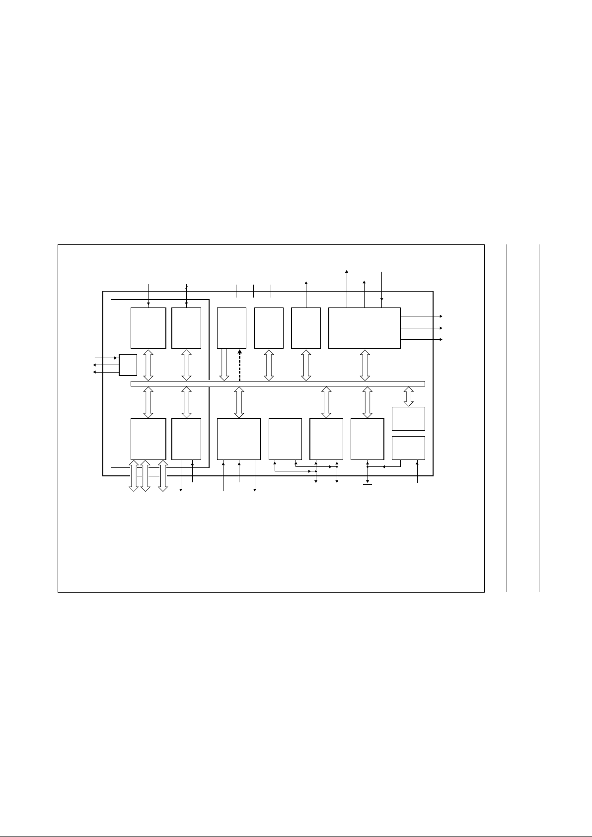
4 BLOCK DIAGRAM
handbook, full pagewidth
MBK981
XTAL1
XTAL2 ACO
TWO 16-BIT
TIMER/
EVENT
COUNTERS
(T0, T1)
CLK
(2)
MOUT2
MOUT1
MOUT0
(3)
PARALLEL
I/O PORTS
P0 P1 P3
(7)
TXD
(4)
T2COMP
(2)
SDA
(2)
SCL
(2)
RXD
(4)
T2
(2)
RST PORENABLE
T2EX
(2)
CPU
8
SERIAL
UART
PORT
DATA
MEMORY
RAM
DTMF
P87CL883
P87CL884
TONE
(1)
RX_MUTE
(6)
TX_MUTE
(6)
MIN
V
DD
V
PP
V
SS
MSK MODEM
8-bit
internal bus
PROGRAM
MEMORY
OTP/ROM
(5)
16-BIT
TIMER/EVENT
COUNTER WITH
CAPTURE/
COMPARE
(T2)
EEPROM
(1)
I
2
C-BUS
INTERFACE
WATCHDOG
TIMER
(T3)
POR
LVD
T0
(4)
INT2 to INT9
(2)
Fig.1 Block diagram.
(1) Only available on the P8xCL884.
(2) Alternative functions of Port 1.
(3) MOUT0 is the alternative function of P3.1.
(4) Alternative functions of Port 3; T0 is only available on the P8xCL883.
(5) In-circuit OTP programming.
(6) By software, any I/O pin can be used.
(7) Port 3: P3.0, P3.1 and P3.4; P3.4 is only available on the P8xCL883.
6
Philips Semiconductors Product specification
TELX microcontrollers for CT0
handset/basestation applications
P8xCL883; P8xCL884
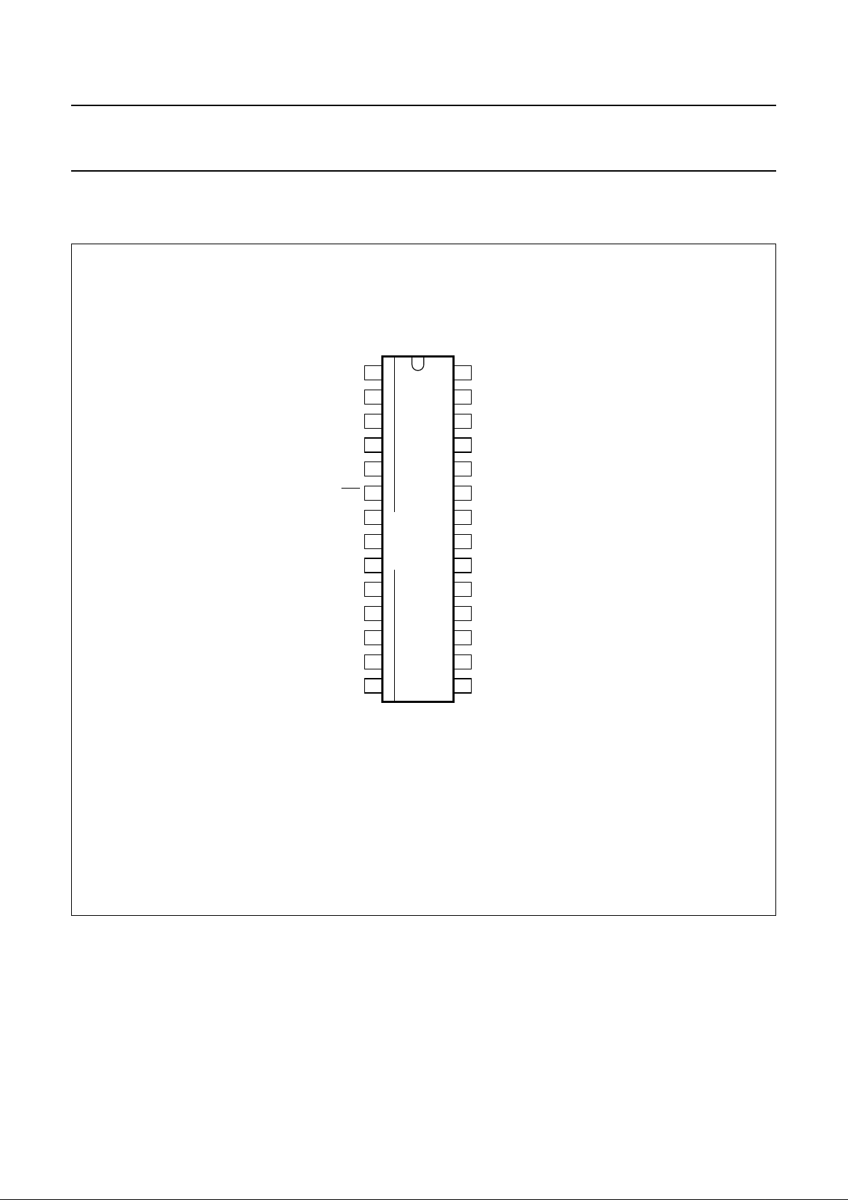
5 PINNING INFORMATION
5.1 Pinning
Fig.2 Pin configuration.
handbook, halfpage
MBK005
1
2
3
4
5
6
7
8
9
10
11
12
13
14
28
27
26
25
24
23
22
21
20
19
18
17
16
15
P0.5 PORENABLE/V
PP
P0.6
P0.7
P3.0/RXD/data
P3.1/TXD/clock/MOUT0
RST
MIN
MOUT1
MOUT2
XTAL1
XTAL2
P1.0/INT2/T2
P1.1/INT3/T2EX
V
DD
P0.4
P0.3
P0.2
P0.1
P0.0
P1.7/INT9/SDA
P1.6/INT8/SCL
P1.5/INT7
P1.4/INT6/CLK
P1.3/INT5
P1.2/INT4/T2COMP
V
SS
P3.4/T0 or TONE
(1)
P83CL883
P83CL884
P87CL883
P87CL884
(1) Pin 20: P3.4/T0 on the P8xCL883; TONE on the P8xCL884.
7
Philips Semiconductors Product specification
TELX microcontrollers for CT0
handset/basestation applications
P8xCL883; P8xCL884
5.2 Pin description
SYMBOL PIN DESCRIPTION
RST 6 Active LOW reset. A LOW level on this pin for two machine cycles while the
oscillator is running, resets the device. The RST pin is also an output which can be
used to reset other ICs.
MIN
7 Digital MSK modem input.
MOUT1
8 Digital MSK modem outputs.
MOUT2
9
XTAL1 10 Crystal input. Input to the Amplitude Controlled Oscillator. Also the input for an
externally generated clock source.
XTAL2 11 Crystal output. Output of the Amplitude Controlled Oscillator. To be left
unconnected when an external oscillator clock is used.
V
DD
14 Power supply.
V
SS
15 Ground.
P0.0 to P0.7
23 to 27,
1to3
Port 0. 8-bit bidirectional I/O port. Every port pin can be used as open-drain,
standard port, high-impedance input or push-pull output, according to Section 6.2.
P1.0/INT2/T2 12 Port 1. 8-bit bidirectional I/O port with alternative functions. Every port pin except
P1.6 and P1.7 (I
2
C-bus pins) can be used as open-drain, standard port,
high-impedance input or push-pull output, according to Section 6.2. Port P1.3 has
LED drive capability.
Port 1 also serves the alternative functions: INT2 to INT9 interrupts; Timer T2
external inputs T2 and T2EX; Timer T2 compare output T2COMP; external clock
output CLK; I
2
C-bus clock SCL and data in/outputs SDA.
P1.1/INT3/T2EX 13
P1.2/INT4/T2COMP 16
P1.3/INT5 17
P1.4/INT6/CLK 18
P1.5/INT7 19
P1.6/INT8/SCL 21
P1.7/INT9/SDA 22
P3.0/RXD/data 4 Port 3. 3 or 2-bit bidirectional I/O port with alternative functions. Every port pin can
be used as open-drain, standard port, high-impedance input or push-pull output,
according to Chapter 6.2.
Port 3 also serves the alternative functions: RXD/data is the serial port receiver
data input (asynchronous) or data I/O (synchronous); TXD/clock is the serial port
transmitter data output (asynchronous) or clock output (synchronous) or digital
MSK modem output MOUT0; T0 is an external input for Timer 0.
P3.4/T0 is only available on the P8xCL883.
P3.1/TXD/clock/
MOUT0
5
P3.4/T0 20
TONE
20 DTMF output; TONE is only available on the P8xCL884.
PORENABLE/V
PP
28 PORENABLE. Power-on reset circuit enable. If PORENABLE = 1, the internal
Power-on reset circuit is enabled. If external reset circuitry is used, it is
recommended to keep PORENABLE = 0 to reach lowest power consumption. This
pin is also used for the OTP programming voltage V
PP
.

8
Philips Semiconductors Product specification
TELX microcontrollers for CT0
handset/basestation applications
P8xCL883; P8xCL884
6 FUNCTIONAL DESCRIPTION
6.1 Special Function Registers (SFRs)
Table 1 List of SFRs
REGISTER
ADDRESS
(HEX)
RESET VALUE
(1)
80C51 core
ACC E0 0000 0000
B F0 0000 0000
DPL 82 0000 0000
DPH 83 0000 0000
PCH no SFR 0000 0000
PCL no SFR 0000 0000
PCON 87 0000 0000
PRESC F3 0000 0000
PSW D0 0000 0000
SP 81 0000 0111
T0/T1
TCON 88 0000 0000
TH0 8C 0000 0000
TH1 8D 0000 0000
TL0 8A 0000 0000
TL1 8B 0000 0000
TMOD 89 0000 0000
Port
ALTP A3 0000 0000
P0 80 1111 1111
P0CFGA 8E 1111 1111
P0CFGB 8F 0000 0000
P1 90 1111 1111
P1CFGA 9E 0011 1111
P1CFGB 9F 0000 0000
P3 B0 XXX1 XX11
P3CFGA BE XXX1 XX11
P3CFGB BF XXX0 XX00
P4 C1 XXXX XXX0
TIMER2
COMP2H AB 0000 0000
COMP2L AA 0000 0000
RCAP2H CB 0000 0000
RCAP2L CA 0000 0000
T2CON C8 0000 0000
TH2 CD 0000 0000
TL2 CC 0000 0000
EEPROM interface
EECON FB 0000 0000
DTMF
HGF A2 0000 0000
LGF A1 0000 0000
Interrupt logic
IEN0 A8 0000 0000
IEN1 E8 0000 0000
IEN2 F1 0000 0000
IP0 B8 0000 0000
IP1 F8 0000 0000
IP2 F9 0000 0000
ISE1 E1 0000 0000
IX1 E9 0000 0000
IRQ1 C0 0000 0000
LVD
LVDCON F2 0000 0000
POR/ACO
RSTAT E6 XXX0 1000
MSK
MCON D3 0000 0000
MBUF D1 XXXX XXXX
MSTAT D2 XX00 0000
UART
S0BUF 99 0000 0000
S0CON 98 0000 0000
I
2
C-bus interface
S1ADR DB 0000 0000
S1CON D8 0000 0000
S1DAT DA 0000 0000
S1STA D9 1111 1000
REGISTER
ADDRESS
(HEX)
RESET VALUE
(1)

9
Philips Semiconductors Product specification
TELX microcontrollers for CT0
handset/basestation applications
P8xCL883; P8xCL884
Note
1. Where: X = undefined state or not implemented bit.
6.2 I/O facilities
6.2.1 PORTS
The P8xCL883/P8xCL884 have 19 and 18 I/O lines
respectively, treated as 19 and 18 individually addressable
bits or as three parallel 8-bit addressable ports.
The alternative functions are detailed below:
Port 0 Offers no alternative functions.
Port 1 Used for a number of special functions:
• P1.0 to P1.7 provides the inputs for the external
interrupts INT2 to INT9
• P1.2/T2COMP for external activation and
Compare/Auto-reload output function of Timer 2
• P1.4/CLK for the clock output
• P1.6/SCL and P1.7/SDA for the I
2
C-bus interface
are real open-drain outputs or high-impedance;
no other port configurations are available.
Port 2 Not available.
Port 3 Pins can be configured individually to provide:
• P3.0/RXD/data and P3.1/TXD/clock/MOUT0
which are serial port receiver input and
transmitter output (UART)
• P3.4/T0 as counter input; available only in
P8xCL883.
To enable a Port pin alternative function, the Port bit latch
in its SFR must contain a logic 1.
WDT
WDCON A5 1010 0101
WDTIM FF 0000 0000
OTP interface
OAH D5 X00X XXXX
OAL D4 XXXX XXXX
ODATA D6 XXXX XXXX
OISYS DC 000X 0000
OTEST D7 0000 0000
Reserved locations; do not write
reserved E7, FD −
REGISTER
ADDRESS
(HEX)
RESET VALUE
(1)
Each port consists of a latch (Special Function Registers
P0 to P3), an output driver and input buffer. All ports have
internal pull-ups. Figure 3b shows that the strong
transistor ‘p1’ is turned on for only one oscillator period
after a LOW-to-HIGH transition in the port latch. When on,
it turns on ‘p3’ (a weak pull-up) through the inverter IN1.
This inverter and transistor ‘p3’ form a latch which holds
the logic 1.
Port P1.3 has LED drive capability.
6.2.2 P
ORT I/O CONFIGURATION
I/O port output configurations are determined by the
settings in port configuration SFRs. There are 2 SFRs for
each port: PnCFGA and PnCFGB, where ‘n’ indicates the
specific port number (0 to 3). One bit in each of the 2 SFRs
relates to the output setting for the corresponding port pin,
allowing any combination of the 2 output types to be mixed
on those port pins. For example, the output type of P1.3, is
controlled by the setting of bit 3 in the SFRs P1CFGA and
P1CFGB.
The port pins may be individually configured via SFRs with
one of the following modes (P1.6 and P1.7 can be
open-drain or high-impedance but never have any diodes
against V
DD
). These modes are also shown in Fig.3.
Mode 0 Open-drain; quasi-bidirectional I/O with
n-channel open-drain output. Use as an output
requires the connection of an external pull-up
resistor; e.g. Port 0 for external memory
accesses (EA = 0) or access above the built-in
memory boundary. The ESD protection diodes
against V
DD
and V
SS
are still present; see Fig.3b.
Except for the I
2
C-bus pins P1.6 and P1.7, ports
which are configured as open-drain still have a
protection diode to V
DD
.
Mode 1 Standard port; quasi-bidirectional I/O with
pull-up. The strong pull-up ‘p1’ is turned on for
only two oscillator periods after a LOW-to-HIGH
transition in the port latch. After these two
oscillator periods the port is only weakly driven
through ‘p2’ and ‘very weakly’ driven through ‘p3’
(see Fig.3b).
Mode 2 High-impedance; this mode turns off all output
drivers on a port. Thus, the pin will not source or
sink current and may be used as an input-only pin
with no internal drivers for an external device to
overcome (see Fig.3c).
Mode 3 Push-pull; output with drive capability in both
polarities. Under this mode, pins can only be
used as outputs (see Fig.3d).

10
Philips Semiconductors Product specification
TELX microcontrollers for CT0
handset/basestation applications
P8xCL883; P8xCL884
Tables 2 and 3 show the configuration register settings for
the 4 port output types.
The electrical characteristics of each output type can be
found in Chapter 8. The default port configuration after
reset is given in Table 3.
Table 2 Port Configuration Registers PnCFGA and PnCFGB (n = 0 to 3) settings
Note
1. Mode changes may cause glitches to occur during transitions. When modifying both registers, WRITE instructions
should be carried out consecutively.
Table 3 Special Function Registers for port configurations/data
Notes
1. This means that P0, P1.0 to P1.5 and P3 are initialized in Mode 1 (quasi-bidirectional, driving a weak HIGH) and the
I
2
C-bus ports P1.6 and P1.7 are initialized in Mode 0 (open-drain, not driven).
2. Port pin P3.4 is only available on P8xCL883.
MODE
(1)
PnCFGA PnCFGB
PORT OUTPUT MODE
NORMAL PORTS I
2
C-BUS PORTS (P1.6 AND P1.7)
Mode 0 0 0 open-drain open-drain
Mode 1 1 0 quasi-bidirectional open-drain
Mode 2 0 1 high-impedance high-impedance
Mode 3 1 1 push-pull open-drain
REGISTER NAME REGISTER MNEMONIC SFR ADDRESS (HEX) STATE AFTER RESET
Port P0 output data
(1)
P0 80 1111 1111
Port P0 configuration A P0CFGA 8E 1111 1111
Port P0 configuration B P0CFGB 8F 0000 0000
Port P1 output data
(1)
P1 90 1111 1111
Port P1 configuration A P1CFGA 9E 0011 1111
Port P1 configuration B P1CFGB 9F 0000 0000
Port P3 output data
(1)
P3 B0 XXX1 XX11
(2)
Port P3 configuration A P3CFGA BE XXX1 XX11
(2)
Port P3 configuration B P3CFGB BF XXX0 XX00
(2)
 Loading...