


Philips P89C51RB2HBA, P89C51RB2HBBD, P89C51RC2HBP, P89C51RC2HBA, P89C51RC2HFA Technical data
...
|
|
|
|
|
|
|
|
|
|
|
|
|
|
|
|
|
|
|
|
|
P89C51RB2 |
INTEGRATED CIRCUITS |
|||||||||||||||||||
|
|
|
|
|
|
|
|
|
|
|
|
|
|
|
|
|
|
|
|
|
|
|
|
|
|
|
|
|
|
|
|
|
|
|
|
|
|
|
|
|
|
|
|
|
|
|
|
|
|
|
|
|
|
|
|
|
|
|
|
|
|
|
|
|
|
|
|
|
|
|
|
|
|
|
|
|
|
|
|
|
|
|
|
|
|
|
|
|
|
|
|
|
|
|
|
|
|
|
|
|
|
|
|
|
|
|
|
|
|
|
|
|
|
|
|
|
|
|
|
|
|
|
|
|
|
P89C51RB2Hxx
P89C51RC2Hxx
P89C51RD2Hxx
80C51 8-bit Flash microcontroller family
16KB/32KB/64KB ISP/IAP Flash with 512B/512B/1KB RAM
Product data |
|
Supersedes data of 2001 Jun 27 |
2002 May 24 |
P s
on o s

Philips Semiconductors Preliminary data
80C51 8-bit Flash microcontroller family |
P89C51RB2/P89C51RC2/ |
16KB/32KB/64KB ISP/IAP Flash with 512B/512B/1KB RAM |
P89C51RD2Hxx |
|
|
DESCRIPTION . . . . . . . . . . . . . . . . . . . . . . . . . . . . . . . . . . . . . . . . . . . . . . . . . . . . . . . . . . . . . . . . . . . . . . . . . . . . . . . . . . . . . . . . . . |
1 |
FEATURES . . . . . . . . . . . . . . . . . . . . . . . . . . . . . . . . . . . . . . . . . . . . . . . . . . . . . . . . . . . . . . . . . . . . . . . . . . . . . . . . . . . . . . . . . . . . . |
1 |
ORDERING INFORMATION . . . . . . . . . . . . . . . . . . . . . . . . . . . . . . . . . . . . . . . . . . . . . . . . . . . . . . . . . . . . . . . . . . . . . . . . . . . . . . . |
2 |
BLOCK DIAGRAM . . . . . . . . . . . . . . . . . . . . . . . . . . . . . . . . . . . . . . . . . . . . . . . . . . . . . . . . . . . . . . . . . . . . . . . . . . . . . . . . . . . . . . . |
3 |
LOGIC SYMBOL . . . . . . . . . . . . . . . . . . . . . . . . . . . . . . . . . . . . . . . . . . . . . . . . . . . . . . . . . . . . . . . . . . . . . . . . . . . . . . . . . . . . . . . . . |
4 |
PINNING . . . . . . . . . . . . . . . . . . . . . . . . . . . . . . . . . . . . . . . . . . . . . . . . . . . . . . . . . . . . . . . . . . . . . . . . . . . . . . . . . . . . . . . . . . . . . . . . |
4 |
Plastic Dual In-Line Package . . . . . . . . . . . . . . . . . . . . . . . . . . . . . . . . . . . . . . . . . . . . . . . . . . . . . . . . . . . . . . . . . . . . . . . . . . . . |
4 |
Plastic Leaded Chip Carrier . . . . . . . . . . . . . . . . . . . . . . . . . . . . . . . . . . . . . . . . . . . . . . . . . . . . . . . . . . . . . . . . . . . . . . . . . . . . . |
4 |
Plastic Quad Flat Pack . . . . . . . . . . . . . . . . . . . . . . . . . . . . . . . . . . . . . . . . . . . . . . . . . . . . . . . . . . . . . . . . . . . . . . . . . . . . . . . . . |
4 |
PIN DESCRIPTIONS . . . . . . . . . . . . . . . . . . . . . . . . . . . . . . . . . . . . . . . . . . . . . . . . . . . . . . . . . . . . . . . . . . . . . . . . . . . . . . . . . . . . . |
5 |
SPECIAL FUNCTION REGISTERS . . . . . . . . . . . . . . . . . . . . . . . . . . . . . . . . . . . . . . . . . . . . . . . . . . . . . . . . . . . . . . . . . . . . . . . . . |
7 |
SPECIAL FUNCTION REGISTERS (CONTINUED) . . . . . . . . . . . . . . . . . . . . . . . . . . . . . . . . . . . . . . . . . . . . . . . . . . . . . . . . . . . |
8 |
OSCILLATOR CHARACTERISTICS . . . . . . . . . . . . . . . . . . . . . . . . . . . . . . . . . . . . . . . . . . . . . . . . . . . . . . . . . . . . . . . . . . . . . . . . |
8 |
RESET . . . . . . . . . . . . . . . . . . . . . . . . . . . . . . . . . . . . . . . . . . . . . . . . . . . . . . . . . . . . . . . . . . . . . . . . . . . . . . . . . . . . . . . . . . . . . . . . . |
8 |
LOW POWER MODES . . . . . . . . . . . . . . . . . . . . . . . . . . . . . . . . . . . . . . . . . . . . . . . . . . . . . . . . . . . . . . . . . . . . . . . . . . . . . . . . . . . |
9 |
Stop Clock Mode . . . . . . . . . . . . . . . . . . . . . . . . . . . . . . . . . . . . . . . . . . . . . . . . . . . . . . . . . . . . . . . . . . . . . . . . . . . . . . . . . . . . . . |
9 |
Idle Mode . . . . . . . . . . . . . . . . . . . . . . . . . . . . . . . . . . . . . . . . . . . . . . . . . . . . . . . . . . . . . . . . . . . . . . . . . . . . . . . . . . . . . . . . . . . . . |
9 |
Power-Down Mode . . . . . . . . . . . . . . . . . . . . . . . . . . . . . . . . . . . . . . . . . . . . . . . . . . . . . . . . . . . . . . . . . . . . . . . . . . . . . . . . . . . . |
9 |
POWER-ON FLAG . . . . . . . . . . . . . . . . . . . . . . . . . . . . . . . . . . . . . . . . . . . . . . . . . . . . . . . . . . . . . . . . . . . . . . . . . . . . . . . . . . . . . . . |
9 |
Design Consideration . . . . . . . . . . . . . . . . . . . . . . . . . . . . . . . . . . . . . . . . . . . . . . . . . . . . . . . . . . . . . . . . . . . . . . . . . . . . . . . . . . |
9 |
ONCEE Mode . . . . . . . . . . . . . . . . . . . . . . . . . . . . . . . . . . . . . . . . . . . . . . . . . . . . . . . . . . . . . . . . . . . . . . . . . . . . . . . . . . . . . . . . . |
9 |
Programmable Clock-Out . . . . . . . . . . . . . . . . . . . . . . . . . . . . . . . . . . . . . . . . . . . . . . . . . . . . . . . . . . . . . . . . . . . . . . . . . . . . . . . |
9 |
TIMER 2 OPERATION . . . . . . . . . . . . . . . . . . . . . . . . . . . . . . . . . . . . . . . . . . . . . . . . . . . . . . . . . . . . . . . . . . . . . . . . . . . . . . . . . . . . |
10 |
Timer 2 . . . . . . . . . . . . . . . . . . . . . . . . . . . . . . . . . . . . . . . . . . . . . . . . . . . . . . . . . . . . . . . . . . . . . . . . . . . . . . . . . . . . . . . . . . . . . . . |
10 |
Capture Mode . . . . . . . . . . . . . . . . . . . . . . . . . . . . . . . . . . . . . . . . . . . . . . . . . . . . . . . . . . . . . . . . . . . . . . . . . . . . . . . . . . . . . . . . . |
10 |
Auto-Reload Mode (Up or Down Counter) . . . . . . . . . . . . . . . . . . . . . . . . . . . . . . . . . . . . . . . . . . . . . . . . . . . . . . . . . . . . . . . . . |
10 |
Baud Rate Generator Mode . . . . . . . . . . . . . . . . . . . . . . . . . . . . . . . . . . . . . . . . . . . . . . . . . . . . . . . . . . . . . . . . . . . . . . . . . . . . . |
13 |
Summary of Baud Rate Equations . . . . . . . . . . . . . . . . . . . . . . . . . . . . . . . . . . . . . . . . . . . . . . . . . . . . . . . . . . . . . . . . . . . . . . . |
14 |
Timer/Counter 2 Set-up . . . . . . . . . . . . . . . . . . . . . . . . . . . . . . . . . . . . . . . . . . . . . . . . . . . . . . . . . . . . . . . . . . . . . . . . . . . . . . . . . |
14 |
Enhanced UART . . . . . . . . . . . . . . . . . . . . . . . . . . . . . . . . . . . . . . . . . . . . . . . . . . . . . . . . . . . . . . . . . . . . . . . . . . . . . . . . . . . . . . . |
15 |
Automatic Address Recognition . . . . . . . . . . . . . . . . . . . . . . . . . . . . . . . . . . . . . . . . . . . . . . . . . . . . . . . . . . . . . . . . . . . . . . . |
15 |
Interrupt Priority Structure . . . . . . . . . . . . . . . . . . . . . . . . . . . . . . . . . . . . . . . . . . . . . . . . . . . . . . . . . . . . . . . . . . . . . . . . . . . . . . . |
18 |
Reduced EMI Mode . . . . . . . . . . . . . . . . . . . . . . . . . . . . . . . . . . . . . . . . . . . . . . . . . . . . . . . . . . . . . . . . . . . . . . . . . . . . . . . . . . . . |
20 |
Reduced EMI Mode . . . . . . . . . . . . . . . . . . . . . . . . . . . . . . . . . . . . . . . . . . . . . . . . . . . . . . . . . . . . . . . . . . . . . . . . . . . . . . . . . . . . |
20 |
AUXR (8EH) . . . . . . . . . . . . . . . . . . . . . . . . . . . . . . . . . . . . . . . . . . . . . . . . . . . . . . . . . . . . . . . . . . . . . . . . . . . . . . . . . . . . . . . |
20 |
Dual DPTR . . . . . . . . . . . . . . . . . . . . . . . . . . . . . . . . . . . . . . . . . . . . . . . . . . . . . . . . . . . . . . . . . . . . . . . . . . . . . . . . . . . . . . . . . . . |
20 |
AUXR1 (A2H) . . . . . . . . . . . . . . . . . . . . . . . . . . . . . . . . . . . . . . . . . . . . . . . . . . . . . . . . . . . . . . . . . . . . . . . . . . . . . . . . . . . . . . |
20 |
DPTR Instructions . . . . . . . . . . . . . . . . . . . . . . . . . . . . . . . . . . . . . . . . . . . . . . . . . . . . . . . . . . . . . . . . . . . . . . . . . . . . . . . . . . . |
20 |
Programmable Counter Array (PCA) . . . . . . . . . . . . . . . . . . . . . . . . . . . . . . . . . . . . . . . . . . . . . . . . . . . . . . . . . . . . . . . . . . . . . . |
21 |
PCA Capture Mode . . . . . . . . . . . . . . . . . . . . . . . . . . . . . . . . . . . . . . . . . . . . . . . . . . . . . . . . . . . . . . . . . . . . . . . . . . . . . . . . . . |
24 |
16-bit Software Timer Mode . . . . . . . . . . . . . . . . . . . . . . . . . . . . . . . . . . . . . . . . . . . . . . . . . . . . . . . . . . . . . . . . . . . . . . . . . . |
24 |
High Speed Output Mode . . . . . . . . . . . . . . . . . . . . . . . . . . . . . . . . . . . . . . . . . . . . . . . . . . . . . . . . . . . . . . . . . . . . . . . . . . . . |
24 |
Pulse Width Modulator Mode . . . . . . . . . . . . . . . . . . . . . . . . . . . . . . . . . . . . . . . . . . . . . . . . . . . . . . . . . . . . . . . . . . . . . . . . . |
24 |
PCA Watchdog Timer . . . . . . . . . . . . . . . . . . . . . . . . . . . . . . . . . . . . . . . . . . . . . . . . . . . . . . . . . . . . . . . . . . . . . . . . . . . . . . . . |
27 |
Expanded Data RAM Addressing . . . . . . . . . . . . . . . . . . . . . . . . . . . . . . . . . . . . . . . . . . . . . . . . . . . . . . . . . . . . . . . . . . . . . . . . |
29 |
HARDWARE WATCHDOG TIMER (ONE-TIME ENABLED WITH RESET-OUT FOR P89C51RB2/RC2/RD2HXX) . . . . |
30 |
Using the WDT . . . . . . . . . . . . . . . . . . . . . . . . . . . . . . . . . . . . . . . . . . . . . . . . . . . . . . . . . . . . . . . . . . . . . . . . . . . . . . . . . . . . . . . . |
30 |
2002 May 24 |
i |

Philips Semiconductors Preliminary data
80C51 8-bit Flash microcontroller family |
P89C51RB2/P89C51RC2/ |
16KB/32KB/64KB ISP/IAP Flash with 512B/512B/1KB RAM |
P89C51RD2Hxx |
|
|
ABSOLUTE MAXIMUM RATINGS . . . . . . . . . . . . . . . . . . . . . . . . . . . . . . . . . . . . . . . . . . . . . . . . . . . . . . . . . . . . . . . . . . . . . . . . . |
31 |
DC ELECTRICAL CHARACTERISTICS . . . . . . . . . . . . . . . . . . . . . . . . . . . . . . . . . . . . . . . . . . . . . . . . . . . . . . . . . . . . . . . . . . . . |
32 |
AC ELECTRICAL CHARACTERISTICS (6 CLOCK MODE) . . . . . . . . . . . . . . . . . . . . . . . . . . . . . . . . . . . . . . . . . . . . . . . . . . . |
33 |
AC ELECTRICAL CHARACTERISTICS (12 CLOCK MODE) . . . . . . . . . . . . . . . . . . . . . . . . . . . . . . . . . . . . . . . . . . . . . . . . . . |
34 |
EXPLANATION OF THE AC SYMBOLS . . . . . . . . . . . . . . . . . . . . . . . . . . . . . . . . . . . . . . . . . . . . . . . . . . . . . . . . . . . . . . . . . . . . |
35 |
FLASH EPROM MEMORY . . . . . . . . . . . . . . . . . . . . . . . . . . . . . . . . . . . . . . . . . . . . . . . . . . . . . . . . . . . . . . . . . . . . . . . . . . . . . . . . |
40 |
GENERAL DESCRIPTION . . . . . . . . . . . . . . . . . . . . . . . . . . . . . . . . . . . . . . . . . . . . . . . . . . . . . . . . . . . . . . . . . . . . . . . . . . . . . . . . |
40 |
FEATURES ± IN-SYSTEM PROGRAMMING (ISP) AND IN-APPLICATION PROGRAMMING (IAP) . . . . . . . . . . . . . . . . |
40 |
CAPABILITIES OF THE PHILIPS 89C51RX2HXX FLASH-BASED MICROCONTROLLERS . . . . . . . . . . . . . . . . . . . . . . . |
40 |
Flash organization . . . . . . . . . . . . . . . . . . . . . . . . . . . . . . . . . . . . . . . . . . . . . . . . . . . . . . . . . . . . . . . . . . . . . . . . . . . . . . . . . . . . . |
40 |
Flash Programming and Erasure . . . . . . . . . . . . . . . . . . . . . . . . . . . . . . . . . . . . . . . . . . . . . . . . . . . . . . . . . . . . . . . . . . . . . . . . . |
40 |
Boot ROM . . . . . . . . . . . . . . . . . . . . . . . . . . . . . . . . . . . . . . . . . . . . . . . . . . . . . . . . . . . . . . . . . . . . . . . . . . . . . . . . . . . . . . . . . . . . |
40 |
Power-On Reset Code Execution . . . . . . . . . . . . . . . . . . . . . . . . . . . . . . . . . . . . . . . . . . . . . . . . . . . . . . . . . . . . . . . . . . . . . . . . |
41 |
Hardware Activation of the Boot Loader . . . . . . . . . . . . . . . . . . . . . . . . . . . . . . . . . . . . . . . . . . . . . . . . . . . . . . . . . . . . . . . . . . . |
41 |
In-System Programming (ISP) . . . . . . . . . . . . . . . . . . . . . . . . . . . . . . . . . . . . . . . . . . . . . . . . . . . . . . . . . . . . . . . . . . . . . . . . . . . |
42 |
Using the In-System Programming (ISP) . . . . . . . . . . . . . . . . . . . . . . . . . . . . . . . . . . . . . . . . . . . . . . . . . . . . . . . . . . . . . . . . . . |
42 |
In Application Programming Method . . . . . . . . . . . . . . . . . . . . . . . . . . . . . . . . . . . . . . . . . . . . . . . . . . . . . . . . . . . . . . . . . . . . . . |
46 |
Using the Watchdog Timer (WDT) . . . . . . . . . . . . . . . . . . . . . . . . . . . . . . . . . . . . . . . . . . . . . . . . . . . . . . . . . . . . . . . . . . . . . |
46 |
Security . . . . . . . . . . . . . . . . . . . . . . . . . . . . . . . . . . . . . . . . . . . . . . . . . . . . . . . . . . . . . . . . . . . . . . . . . . . . . . . . . . . . . . . . . . . . . . |
48 |
REVISION HISTORY . . . . . . . . . . . . . . . . . . . . . . . . . . . . . . . . . . . . . . . . . . . . . . . . . . . . . . . . . . . . . . . . . . . . . . . . . . . . . . . . . . . . . |
52 |
2002 May 24 |
ii |

Philips Semiconductors Product data
80C51 8-bit Flash microcontroller family |
P89C51RB2/P89C51RC2/ |
16KB/32KB/64KB ISP/IAP Flash with 512B/512B/1KB RAM |
P89C51RD2Hxx |
|
|
|
|
DESCRIPTION
The P89C51RB2/RC2/RD2Hxx device contains a non-volatile 16KB/32KB/64KB Flash program memory that is both parallel programmable and serial In-System and In-Application Programmable. In-System Programming (ISP) allows the user to download new code while the microcontroller sits in the application. In-Application Programming (IAP) means that the microcontroller fetches new program code and reprograms itself while in the system. This allows for remote programming over a modem link.
A default serial loader (boot loader) program in ROM allows serial
In-System programming of the Flash memory via the UART without the need for a loader in the Flash code. For In-Application Programming, the user program erases and reprograms the Flash memory by use of standard routines contained in ROM.
This device executes one machine cycle in 6 clock cycles, hence providing twice the speed of a conventional 80C51. An OTP configuration bit lets the user select conventional 12 clock timing if desired.
This device is a Single-Chip 8-Bit Microcontroller manufactured in advanced CMOS process and is a derivative of the 80C51 microcontroller family. The instruction set is 100% compatible with the 80C51 instruction set.
The device also has four 8-bit I/O ports, three 16-bit timer/event counters, a multi-source, four-priority-level, nested interrupt structure, an enhanced UART and on-chip oscillator and timing circuits.
The added features of the P89C51RB2/RC2/RD2Hxx makes it a powerful microcontroller for applications that require pulse width modulation, high-speed I/O and up/down counting capabilities such as motor control.
FEATURES
•80C51 Central Processing Unit
•On-chip Flash Program Memory with In-System Programming
(ISP) and In-Application Programming (IAP) capability
•Boot ROM contains low level Flash programming routines for downloading via the UART
•Can be programmed by the end-user application (IAP)
•Parallel programming with 87C51 compatible hardware interface to programmer
•Six clocks per machine cycle operation (standard)
•12 clocks per machine cycle operation (optional)
•Speed up to 20 MHz with 6 clock cycles per machine cycle
(40 MHz equivalent performance); up to 33 MHz with 12 clocks per machine cycle
•Fully static operation
•RAM expandable externally to 64 kbytes
•Four interrupt priority levels
•Seven interrupt sources
•Four 8-bit I/O ports
•Full-duplex enhanced UART
±Framing error detection
±Automatic address recognition
•Power control modes
±Clock can be stopped and resumed
±Idle mode
±Power down mode
•Programmable clock out
•Second DPTR register
•Asynchronous port reset
•Low EMI (inhibit ALE)
•Programmable Counter Array (PCA)
±PWM
±Capture/compare
2002 May 24 |
1 |
853-2349 28312 |

Philips Semiconductors Product data
80C51 8-bit Flash microcontroller family |
|
P89C51RB2/P89C51RC2/ |
||||||
16KB/32KB/64KB ISP/IAP Flash with 512B/512B/1KB RAM |
|
P89C51RD2Hxx |
||||||
|
|
|
|
|
|
|
|
|
ORDERING INFORMATION |
|
|
|
|
|
|
||
|
|
|
|
|
|
|
|
|
|
PART ORDER |
MEMORY |
TEMPERATURE |
VOLTAGE |
FREQUENCY (MHz) |
|
||
|
FLASH |
RAM |
RANGE (°C) |
6 CLOCK |
12 CLOCK |
DWG # |
||
|
NUMBER |
RANGE |
||||||
|
AND PACKAGE |
|
||||||
|
|
|
MODE |
MODE |
|
|||
|
|
|
|
|
|
|||
|
|
|
|
|
|
|
||
1 |
P89C51RB2HBA |
16 kB |
512 B |
0 to +70, PLCC |
4.5±5.5 V |
0 to 20 MHz |
0 to 33 MHz |
SOT187-2 |
|
|
|
|
|
|
|
|
|
2 |
P89C51RB2HBBD |
16 kB |
512 B |
0 to +70, LQFP |
4.5±5.5 V |
0 to 20 MHz |
0 to 33 MHz |
SOT389-1 |
|
|
|
|
|
|
|
|
|
3 |
P89C51RC2HBP |
32 kB |
512 B |
0 to +70, PDIP |
4.5±5.5 V |
0 to 20 MHz |
0 to 33 MHz |
SOT129-1 |
|
|
|
|
|
|
|
|
|
4 |
P89C51RC2HBA |
32 kB |
512 B |
0 to +70, PLCC |
4.5±5.5 V |
0 to 20 MHz |
0 to 33 MHz |
SOT187-2 |
|
|
|
|
|
|
|
|
|
5 |
P89C51RC2HFA |
32 kB |
512 B |
±40 to +85, PLCC |
4.75±5.25 V |
0 to 20 MHz |
0 to 33 MHz |
SOT187-2 |
|
|
|
|
|
|
|
|
|
6 |
P89C51RC2HBBD |
32 kB |
512 B |
0 to +70, LQFP |
4.5±5.5 V |
0 to 20 MHz |
0 to 33 MHz |
SOT389-1 |
|
|
|
|
|
|
|
|
|
7 |
P89C51RC2HFBD |
32 kB |
512 B |
±40 to +85, LQFP |
4.75±5.25 V |
0 to 20 MHz |
0 to 33 MHz |
SOT389-1 |
|
|
|
|
|
|
|
|
|
8 |
P89C51RD2HBP |
64 kB |
1 kB |
0 to +70, PDIP |
4.5±5.5 V |
0 to 20 MHz |
0 to 33 MHz |
SOT129-1 |
|
|
|
|
|
|
|
|
|
9 |
P89C51RD2HBA |
64 kB |
1 kB |
0 to +70, PLCC |
4.5±5.5 V |
0 to 20 MHz |
0 to 33 MHz |
SOT187-2 |
|
|
|
|
|
|
|
|
|
10 |
P89C51RD2HBBD |
64 kB |
1 kB |
0 to +70, LQFP |
4.5±5.5 V |
0 to 20 MHz |
0 to 33 MHz |
SOT389-1 |
|
|
|
|
|
|
|
|
|
2002 May 24 |
2 |

Philips Semiconductors Product data
80C51 8-bit Flash microcontroller family |
P89C51RB2/P89C51RC2/ |
16KB/32KB/64KB ISP/IAP Flash with 512B/512B/1KB RAM |
P89C51RD2Hxx |
|
|
BLOCK DIAGRAM
|
|
|
|
P0.0±P0.7 |
P2.0±P2.7 |
|
|
|
|
|
|
PORT 0 |
PORT 2 |
|
|
|
|
|
|
DRIVERS |
DRIVERS |
|
|
VCC |
|
|
|
|
|
|
|
VSS |
|
|
|
|
|
|
|
|
RAM ADDR |
RAM |
PORT 0 |
PORT 2 |
FLASH |
|
|
|
REGISTER |
|
LATCH |
LATCH |
|
|
|
|
|
|
|
|
|
|
8 |
|
B |
|
ACC |
|
|
STACK |
|
|
REGISTER |
|
|
|
POINTER |
|
|
|
|
|
|
|
|
||
|
|
|
|
|
|
|
PROGRAM |
|
|
|
|
|
TMP1 |
|
ADDRESS |
|
|
|
|
TMP2 |
|
REGISTER |
|
|
|
|
|
ALU |
|
|
BUFFER |
|
|
|
|
|
|
|
|
|
|
|
|
|
SFRs |
|
|
|
|
|
|
|
TIMERS |
|
PC |
|
|
|
|
|
|
|
|
|
|
|
|
PSW |
P.C.A. |
|
INCRE- |
|
|
|
|
|
|
MENTER |
|
|
|
|
|
|
|
|
|
|
|
|
|
|
|
8 |
16 |
|
|
|
|
|
|
|
PROGRAM |
|
|
|
|
|
|
|
COUNTER |
PSEN |
|
INSTRUCTION |
REGISTER |
|
|
|
|
ALE |
TIMING |
|
|
|
DPTR'S |
||
EAVPP |
AND |
|
|
|
MULTIPLE |
||
CONTROL |
|
|
|
|
|||
RST |
|
|
|
|
|
||
|
PD |
|
|
PORT 1 |
|
PORT 3 |
|
|
|
|
|
LATCH |
|
LATCH |
|
|
OSCILLATOR |
|
|
|
|
||
|
|
|
|
PORT 1 |
|
PORT 3 |
|
|
|
|
|
DRIVERS |
|
DRIVERS |
|
|
XTAL1 |
|
XTAL2 |
|
|
|
|
|
|
|
|
P1.0±P1.7 |
|
P3.0±P3.7 |
|
|
|
|
|
|
|
|
SU01065 |
2002 May 24 |
|
|
|
|
3 |
|
|
Philips Semiconductors Product data
80C51 8-bit Flash microcontroller family |
P89C51RB2/P89C51RC2/ |
16KB/32KB/64KB ISP/IAP Flash with 512B/512B/1KB RAM |
P89C51RD2Hxx |
|
|
LOGIC SYMBOL
|
|
VCC |
VSS |
|
|
|
XTAL1 |
|
|
|
|
|
0 |
ADDRESS AND |
|
|
|
PORT |
DATA BUS |
|
|
|
|
|
|
|
XTAL2 |
|
|
|
|
|
|
T2 |
|
|
|
1 |
T2EX |
|
|
RST |
|
|
|
|
PORT |
|
|
|
|
EA/VPP |
|
|
|
|
|
|
|
|
|
PSEN |
|
|
FUNCTIONSSECONDARY |
ALE/PROG |
2PORT |
|
|
RxD |
3PORT |
|
||
|
|
|
|
|
|
TxD |
|
|
|
|
INT0 |
|
|
|
|
INT1 |
|
|
ADDRESS BUS |
|
T0 |
|
|
|
|
|
|
|
|
|
T1 |
|
|
|
|
WR |
|
|
|
|
RD |
|
|
|
|
|
|
|
SU01302 |
PINNING
Plastic Dual In-Line Package
|
T2/P1.0 |
|
|
|
|
|
|
VCC |
||||
|
1 |
|
|
|
40 |
|
||||||
T2EX/P1.1 |
|
|
|
|
|
|
|
|
|
|
||
2 |
|
|
|
39 |
|
P0.0/AD0 |
||||||
|
ECI/P1.2 |
|
|
|
|
|
|
|
|
|
|
|
|
3 |
|
|
|
38 |
|
P0.1/AD1 |
|||||
|
|
|
|
|
|
|
|
|
|
|
|
|
CEX0/P1.3 |
4 |
|
|
|
37 |
|
P0.2/AD2 |
|||||
CEX1/P1.4 |
|
|
|
|
|
|
|
|
|
|
||
|
|
|
|
|
|
|
|
|
|
|||
5 |
|
|
|
36 |
|
P0.3/AD3 |
||||||
|
|
|
|
|
|
|
|
|
|
|
|
|
CEX2/P1.5 |
6 |
|
|
|
35 |
|
P0.4/AD4 |
|||||
|
|
|
|
|
|
|
|
|
|
|
|
|
CEX3/P1.6 |
7 |
|
|
|
34 |
|
P0.5/AD5 |
|||||
|
|
|
|
|
|
|
|
|
|
|
|
|
CEX4/P1.7 |
8 |
|
|
|
33 |
|
P0.6/AD6 |
|||||
|
|
|
|
|
|
|
|
|
|
|
|
|
|
|
RST |
9 |
|
|
|
32 |
|
P0.7/AD7 |
|||
|
|
|
|
|
DUAL |
|
|
|
|
|
|
|
|
|
|
|
|
|
|
|
|
|
|
||
|
RxD/P3.0 |
10 |
|
31 |
|
EA/VPP |
||||||
|
|
|
|
IN-LINE |
|
|
|
|
|
|
||
|
TxD/P3.1 |
11 |
PACKAGE |
30 |
|
|
|
|
||||
|
|
ALE/PROG |
||||||||||
|
|
|
|
|
|
|
|
|
|
|
|
|
|
|
|
12 |
|
|
|
29 |
|
|
|
|
|
|
INT0/P3.2 |
|
|
|
|
PSEN |
||||||
|
|
|
|
|
|
|
|
|
|
|
|
|
|
|
|
13 |
|
|
|
28 |
|
P2.7/A15 |
|||
|
INT1/P3.3 |
|
|
|
||||||||
|
|
|
|
|
|
|
|
|
|
|
|
|
|
T0/P3.4 |
14 |
|
|
|
27 |
|
P2.6/A14 |
||||
|
|
|
|
|
|
|
|
|
|
|
|
|
|
T1/P3.5 |
15 |
|
|
|
26 |
|
P2.5/A13 |
||||
|
|
|
|
|
|
|
|
|
|
|
|
|
|
|
|
16 |
|
|
|
25 |
|
P2.4/A12 |
|||
|
WR/P3.6 |
|
|
|
||||||||
|
|
|
|
|
|
|
|
|
|
|
|
|
|
|
|
17 |
|
|
|
24 |
|
P2.3/A11 |
|||
|
RD/P3.7 |
|
|
|
||||||||
|
|
|
|
|
|
|
|
|
|
|
|
|
|
XTAL2 |
18 |
|
|
|
23 |
|
P2.2/A10 |
||||
|
|
|
|
|
|
|
|
|
|
|
|
|
|
XTAL1 |
19 |
|
|
|
22 |
|
P2.1/A9 |
||||
|
|
|
|
|
|
|
|
|
|
|
|
|
|
|
VSS |
20 |
|
|
|
21 |
|
P2.0/A8 |
|||
|
|
|
|
|
|
|
|
|
|
|
|
|
Plastic Leaded Chip Carrier
6 |
1 |
40 |
7 |
|
39 |
|
LCC |
|
17 |
|
29 |
18 |
|
28 |
Pin |
Function |
Pin |
Function |
Pin |
Function |
||||||||
1 |
NIC* |
16 |
P3.4/T0 |
31 |
P2.7/A15 |
||||||||
2 |
P1.0/T2 |
17 |
P3.5/T1 |
32 |
|
|
|
|
|||||
PSEN |
|||||||||||||
3 |
P1.1/T2EX |
18 |
|
|
|
|
|
|
|
|
|
||
P3.6/WR |
|
33 |
ALE/PROG |
||||||||||
4 |
P1.2/ECI |
19 |
|
|
|
34 |
NIC* |
||||||
P3.7/RD |
|
||||||||||||
5 |
P1.3/CEX0 |
20 |
XTAL2 |
35 |
|
|
|||||||
EA/VPP |
|||||||||||||
6 |
P1.4/CEX1 |
21 |
XTAL1 |
36 |
P0.7/AD7 |
||||||||
7 |
P1.5/CEX2 |
22 |
VSS |
37 |
P0.6/AD6 |
||||||||
8 |
P1.6/CEX3 |
23 |
NIC* |
38 |
P0.5/AD5 |
||||||||
9 |
P1.7/CEX4 |
24 |
P2.0/A8 |
39 |
P0.4/AD4 |
||||||||
10 |
RST |
25 |
P2.1/A9 |
40 |
P0.3/AD3 |
||||||||
11 |
P3.0/RxD |
26 |
P2.2/A10 |
41 |
P0.2/AD2 |
||||||||
12 |
NIC* |
27 |
P2.3/A11 |
42 |
P0.1/AD1 |
||||||||
13 |
P3.1/TxD |
28 |
P2.4/A12 |
43 |
P0.0/AD0 |
||||||||
14 |
|
|
|
29 |
P2.5/A13 |
44 |
VCC |
||||||
P3.2/INT0 |
|
||||||||||||
15 |
|
|
|
30 |
P2.6/A14 |
|
|
|
|
|
|||
P3.3/INT1 |
|
|
|
|
|
|
|||||||
* NO INTERNAL CONNECTION |
|
|
|
|
|
SU00023 |
|||||||
Plastic Quad Flat Pack
|
|
|
|
|
|
|
|
44 |
|
|
|
|
34 |
|
|
|
|||||
|
1 |
|
|
|
|
|
|
|
|
|
|
|
|
|
33 |
|
|||||
|
|
|
|
|
|
|
|
|
|
|
|
|
|
|
|
||||||
|
|
|
|
|
|
LQFP |
|
|
|
|
|||||||||||
|
|
|
|
|
|
|
|
||||||||||||||
|
|
|
|
|
|
|
|
||||||||||||||
|
|
|
|
|
|
|
|
|
|
|
|
|
|
|
|
|
|
||||
|
11 |
|
|
12 |
|
|
|
|
22 |
|
23 |
|
|||||||||
|
|
|
|
|
|
|
|
|
|||||||||||||
|
|
|
|
|
|
|
|
|
|||||||||||||
|
|
|
|
|
|
|
|
|
|||||||||||||
|
|
|
|
|
|
|
|
|
|
|
|
|
|
|
|||||||
Pin |
Function |
Pin |
Function |
|
|
|
|
Pin |
Function |
||||||||||||
1 |
P1.5/CEX2 |
16 |
VSS |
31 |
P0.6/AD6 |
||||||||||||||||
2 |
P1.6/CEX3 |
17 |
NIC* |
32 |
P0.5/AD5 |
||||||||||||||||
3 |
P1.7/CEX4 |
18 |
P2.0/A8 |
33 |
P0.4/AD4 |
||||||||||||||||
4 |
RST |
19 |
P2.1/A9 |
34 |
P0.3/AD3 |
||||||||||||||||
5 |
P3.0/RxD |
20 |
P2.2/A10 |
35 |
P0.2/AD2 |
||||||||||||||||
6 |
NIC* |
21 |
P2.3/A11 |
36 |
P0.1/AD1 |
||||||||||||||||
7 |
P3.1/TxD |
22 |
P2.4/A12 |
37 |
P0.0/AD0 |
||||||||||||||||
8 |
|
|
|
|
|
23 |
P2.5/A13 |
38 |
VCC |
||||||||||||
P3.2/INT0 |
|
||||||||||||||||||||
9 |
|
|
|
|
|
24 |
P2.6/A14 |
39 |
NIC* |
||||||||||||
P3.3/INT1 |
|
||||||||||||||||||||
10 |
P3.4/T0 |
25 |
P2.7/A15 |
40 |
P1.0/T2 |
||||||||||||||||
11 |
P3.5/T1 |
26 |
|
|
|
|
41 |
P1.1/T2EX |
|||||||||||||
PSEN |
|||||||||||||||||||||
12 |
|
|
|
|
27 |
|
|
|
|
42 |
P1.2/ECI |
||||||||||
P3.6/WR |
|
ALE/PROG |
|||||||||||||||||||
13 |
|
|
|
28 |
NIC* |
43 |
P1.3/CEX0 |
||||||||||||||
P3.7/RD |
|
||||||||||||||||||||
14 |
XTAL2 |
29 |
|
|
44 |
P1.4/CEX1 |
|||||||||||||||
EA/VPP |
|||||||||||||||||||||
15 |
XTAL1 |
30 |
P0.7/AD7 |
|
|
|
|
|
|
|
|||||||||||
* NO INTERNAL CONNECTION |
|
|
|
|
|
|
|
|
|
|
|
|
|
SU01400 |
|||||||
|
|
|
|
|
|
|
|
|
|
|
|
|
|
|
|
|
|
|
|
|
|
SU00021
2002 May 24 |
4 |

Philips Semiconductors Product data
80C51 8-bit Flash microcontroller family |
P89C51RB2/P89C51RC2/ |
16KB/32KB/64KB ISP/IAP Flash with 512B/512B/1KB RAM |
P89C51RD2Hxx |
|
|
PIN DESCRIPTIONS
MNEMONIC |
|
PIN NUMBER |
|
TYPE |
|
|
|
|
|
NAME AND FUNCTION |
||
|
|
|
|
|
|
|
|
|
|
|||
PDIP |
|
PLCC |
|
LQFP |
||||||||
|
|
|
|
|
|
|
|
|
|
|||
|
|
|
|
|
|
|
|
|
|
|
|
|
VSS |
20 |
|
22 |
|
16 |
I |
Ground: 0 V reference. |
|||||
VCC |
40 |
|
44 |
|
38 |
I |
Power Supply: This is the power supply voltage for normal, idle, and power-down |
|||||
|
|
|
|
|
|
|
operation. |
|||||
P0.0±0.7 |
39±32 |
|
43±36 |
|
37±30 |
I/O |
Port 0: Port 0 is an open-drain, bidirectional I/O port. Port 0 pins that have 1s |
|||||
|
|
|
|
|
|
|
written to them float and can be used as high-impedance inputs. Port 0 is also the |
|||||
|
|
|
|
|
|
|
multiplexed low-order address and data bus during accesses to external program |
|||||
|
|
|
|
|
|
|
and data memory. In this application, it uses strong internal pull-ups when emitting 1s. |
|||||
P1.0±P1.7 |
1±8 |
|
2±9 |
|
40±44, |
I/O |
Port 1: Port 1 is an 8-bit bidirectional I/O port with internal pull-ups on all pins. |
|||||
|
|
|
|
|
1±3 |
|
Port 1 pins that have 1s written to them are pulled high by the internal pull-ups and |
|||||
|
|
|
|
|
|
|
can be used as inputs. As inputs, port 1 pins that are externally pulled low will |
|||||
|
|
|
|
|
|
|
source current because of the internal pull-ups. (See DC Electrical Characteristics: |
|||||
|
|
|
|
|
|
|
IIL). |
|||||
|
|
|
|
|
|
|
Alternate functions for P89C51RB2/RC2/RD2Hxx Port 1 include: |
|||||
|
1 |
|
2 |
|
40 |
I/O |
|
T2 (P1.0): Timer/Counter 2 external count input/Clockout (see Programmable |
||||
|
|
|
|
|
|
|
|
Clock-Out) |
||||
|
2 |
|
3 |
|
41 |
I |
|
T2EX (P1.1): Timer/Counter 2 Reload/Capture/Direction Control |
||||
|
3 |
|
4 |
|
42 |
I |
|
ECI (P1.2): External Clock Input to the PCA |
||||
|
4 |
|
5 |
|
43 |
I/O |
|
CEX0 (P1.3): Capture/Compare External I/O for PCA module 0 |
||||
|
5 |
|
6 |
|
44 |
I/O |
|
CEX1 (P1.4): Capture/Compare External I/O for PCA module 1 |
||||
|
6 |
|
7 |
|
1 |
I/O |
|
CEX2 (P1.5): Capture/Compare External I/O for PCA module 2 |
||||
|
7 |
|
8 |
|
2 |
I/O |
|
CEX3 (P1.6): Capture/Compare External I/O for PCA module 3 |
||||
|
8 |
|
9 |
|
3 |
I/O |
|
CEX4 (P1.7): Capture/Compare External I/O for PCA module 4 |
||||
P2.0±P2.7 |
21±28 |
|
24±31 |
|
18±25 |
I/O |
Port 2: Port 2 is an 8-bit bidirectional I/O port with internal pull-ups. Port 2 pins that |
|||||
|
|
|
|
|
|
|
have 1s written to them are pulled high by the internal pull-ups and can be used as |
|||||
|
|
|
|
|
|
|
inputs. As inputs, port 2 pins that are externally being pulled low will source current |
|||||
|
|
|
|
|
|
|
because of the internal pull-ups. (See DC Electrical Characteristics: IIL). Port 2 |
|||||
|
|
|
|
|
|
|
emits the high-order address byte during fetches from external program memory |
|||||
|
|
|
|
|
|
|
and during accesses to external data memory that use 16-bit addresses (MOVX |
|||||
|
|
|
|
|
|
|
@DPTR). In this application, it uses strong internal pull-ups when emitting 1s. |
|||||
|
|
|
|
|
|
|
During accesses to external data memory that use 8-bit addresses (MOV @Ri), |
|||||
|
|
|
|
|
|
|
port 2 emits the contents of the P2 special function register. |
|||||
|
|
|
|
|
|
|
P2.7 must be a ªIº to program and erase the device. |
|||||
P3.0±P3.7 |
10±17 |
|
11, |
|
5, 7±13 |
I/O |
Port 3: Port 3 is an 8-bit bidirectional I/O port with internal pull-ups. Port 3 pins that |
|||||
|
|
|
13±19 |
|
|
|
have 1s written to them are pulled high by the internal pull-ups and can be used as |
|||||
|
|
|
|
|
|
|
inputs. As inputs, port 3 pins that are externally being pulled low will source current |
|||||
|
|
|
|
|
|
|
because of the pull-ups. (See DC Electrical Characteristics: IIL). Port 3 also serves |
|||||
|
|
|
|
|
|
|
the special features of the P89C51RB2/RC2/RD2Hxx, as listed below: |
|||||
|
10 |
|
11 |
|
5 |
I |
|
RxD (P3.0): Serial input port |
||||
|
11 |
|
13 |
|
7 |
O |
|
TxD (P3.1): Serial output port |
||||
|
12 |
|
14 |
|
8 |
I |
|
|
|
|
|
(P3.2): External interrupt |
|
|
|
|
INT0 |
||||||||
|
13 |
|
15 |
|
9 |
I |
|
|
|
|
(P3.3): External interrupt |
|
|
|
|
|
INT1 |
||||||||
|
14 |
|
16 |
|
10 |
I |
|
T0 (P3.4): Timer 0 external input |
||||
|
15 |
|
17 |
|
11 |
I |
|
T1 (P3.5): Timer 1 external input |
||||
|
16 |
|
18 |
|
12 |
O |
|
|
|
(P3.6): External data memory write strobe |
||
|
|
|
|
WR |
||||||||
|
17 |
|
19 |
|
13 |
O |
|
|
(P3.7): External data memory read strobe |
|||
|
|
|
|
RD |
||||||||
RST |
9 |
|
10 |
|
4 |
I |
Reset: A high on this pin for two machine cycles while the oscillator is running, |
|||||
|
|
|
|
|
|
|
resets the device. An internal resistor to VSS permits a power-on reset using only |
|||||
|
|
|
|
|
|
|
an external capacitor to VCC. |
|||||
ALE |
30 |
|
33 |
|
27 |
O |
Address Latch Enable: Output pulse for latching the low byte of the address |
|||||
|
|
|
|
|
|
|
during an access to external memory. In normal operation, ALE is emitted twice |
|||||
|
|
|
|
|
|
|
every machine cycle, and can be used for external timing or clocking. Note that one |
|||||
|
|
|
|
|
|
|
ALE pulse is skipped during each access to external data memory. ALE can be |
|||||
|
|
|
|
|
|
|
disabled by setting SFR auxiliary.0. With this bit set, ALE will be active only during a |
|||||
|
|
|
|
|
|
|
MOVX instruction. |
|||||
2002 May 24 |
5 |

Philips Semiconductors Product data
|
80C51 8-bit Flash microcontroller family |
|
|
P89C51RB2/P89C51RC2/ |
|||||||||||||||||||
|
16KB/32KB/64KB ISP/IAP Flash with 512B/512B/1KB RAM |
|
|
|
|
P89C51RD2Hxx |
|||||||||||||||||
|
|
|
|
|
|
|
|
|
|
|
|
|
|
|
|
|
|
|
|
|
|
|
|
|
|
|
|
|
|
|
|
|
|
|
|
|
|
|
|
|
|
|
|
|
|
|
|
|
MNEMONIC |
|
PIN NUMBER |
|
TYPE |
|
|
|
|
|
|
NAME AND FUNCTION |
|||||||||||
|
|
|
|
|
|
|
|
|
|
|
|
||||||||||||
PDIP |
|
PLCC |
|
LQFP |
|
|
|
|
|
|
|||||||||||||
|
|
|
|
|
|
|
|
|
|
|
|
|
|
|
|
|
|
|
|
|
|||
|
|
|
|
|
|
|
|
|
|
|
|
|
|
|
|
|
|||||||
|
|
|
|
29 |
|
32 |
|
26 |
O |
Program Store Enable: The read strobe to external program memory. When |
|||||||||||||
|
PSEN |
|
|
||||||||||||||||||||
|
|
|
|
|
|
|
|
|
|
executing code from the external program memory, |
PSEN |
is activated twice each |
|||||||||||
|
|
|
|
|
|
|
|
|
|
machine cycle, except that two |
PSEN |
activations are skipped during each access |
|||||||||||
|
|
|
|
|
|
|
|
|
|
to external data memory. |
PSEN |
is not activated during fetches from internal |
|||||||||||
|
|
|
|
|
|
|
|
|
|
program memory. |
|
|
|
|
|
|
|
|
|||||
|
|
|
|
|
|
|
|
|
|
|
|||||||||||||
|
|
|
|
31 |
|
35 |
|
29 |
I |
External Access Enable/Programming Supply Voltage: |
|
must be externally |
|||||||||||
|
EA/VPP |
|
|
EA |
|||||||||||||||||||
|
|
|
|
|
|
|
|
|
|
held low to enable the device to fetch code from external program memory |
|||||||||||||
|
|
|
|
|
|
|
|
|
|
locations. If |
EA |
is held high, the device executes from internal program memory. |
|||||||||||
|
|
|
|
|
|
|
|
|
|
The value on the |
EA |
pin is latched when RST is released and any subsequent |
|||||||||||
|
|
|
|
|
|
|
|
|
|
changes have no effect. This pin also receives the programming supply voltage |
|||||||||||||
|
|
|
|
|
|
|
|
|
|
(VPP) during Flash programming. |
|||||||||||||
|
XTAL1 |
19 |
|
21 |
|
15 |
I |
Crystal 1: Input to the inverting oscillator amplifier and input to the internal clock |
|||||||||||||||
|
|
|
|
|
|
|
|
|
|
generator circuits. |
|
|
|
|
|
|
|
|
|||||
|
|
|
|
|
|
|
|
|
|||||||||||||||
|
XTAL2 |
18 |
|
20 |
|
14 |
O |
Crystal 2: Output from the inverting oscillator amplifier. |
|||||||||||||||
NOTE: |
) must not be higher than V |
|
+ 0.5 V or less than V |
|
± 0.5 V. |
To avoid ªlatch-upº effect at power-on, the voltage on any pin (other than V |
CC |
SS |
|||
PP |
|
|
|||
2002 May 24 |
6 |

Philips Semiconductors Product data
80C51 8-bit Flash microcontroller family |
P89C51RB2/P89C51RC2/ |
16KB/32KB/64KB ISP/IAP Flash with 512B/512B/1KB RAM |
P89C51RD2Hxx |
|
|
SPECIAL FUNCTION REGISTERS
SYMBOL |
DESCRIPTION |
DIRECT |
|
BIT ADDRESS, SYMBOL, OR ALTERNATIVE PORT FUNCTION |
RESET |
||||||||||||||
ADDRESS |
MSB |
|
|
|
|
|
|
|
|
|
|
|
|
LSB |
VALUE |
||||
|
|
|
|
|
|
|
|
|
|
|
|
|
|
||||||
|
|
|
|
|
|
|
|
|
|
|
|
|
|
|
|
|
|
|
|
ACC* |
Accumulator |
E0H |
|
E7 |
|
E6 |
E5 |
E4 |
|
E3 |
|
E2 |
E1 |
E0 |
00H |
||||
|
|
|
|
|
|
|
|
|
|
|
|
|
|
|
|
|
|
|
|
AUXR# |
Auxiliary |
8EH |
± |
|
± |
|
± |
± |
± |
|
± |
|
EXTRAM |
AO |
xxxxxx00B |
||||
|
|
|
|
|
|
|
|
|
|
|
|
|
|
|
|
|
|
|
|
AUXR1# |
Auxiliary 1 |
A2H |
± |
|
± |
|
ENBOOT |
± |
|
GF2 |
0 |
|
± |
DPS |
xxxxxxx0B |
||||
|
|
|
|
|
|
|
|
|
|
|
|
|
|
|
|
|
|
|
|
B* |
B register |
F0H |
|
F7 |
|
F6 |
F5 |
F4 |
|
F3 |
|
F2 |
F1 |
F0 |
00H |
||||
CCAP0H# |
Module 0 Capture High |
FAH |
|
|
|
|
|
|
|
|
|
|
|
|
|
|
|
|
xxxxxxxxB |
CCAP1H# |
Module 1 Capture High |
FBH |
|
|
|
|
|
|
|
|
|
|
|
|
|
|
|
|
xxxxxxxxB |
CCAP2H# |
Module 2 Capture High |
FCH |
|
|
|
|
|
|
|
|
|
|
|
|
|
|
|
|
xxxxxxxxB |
CCAP3H# |
Module 3 Capture High |
FDH |
|
|
|
|
|
|
|
|
|
|
|
|
|
|
|
|
xxxxxxxxB |
CCAP4H# |
Module 4 Capture High |
FEH |
|
|
|
|
|
|
|
|
|
|
|
|
|
|
|
|
xxxxxxxxB |
CCAP0L# |
Module 0 Capture Low |
EAH |
|
|
|
|
|
|
|
|
|
|
|
|
|
|
|
|
xxxxxxxxB |
CCAP1L# |
Module 1 Capture Low |
EBH |
|
|
|
|
|
|
|
|
|
|
|
|
|
|
|
|
xxxxxxxxB |
CCAP2L# |
Module 2 Capture Low |
ECH |
|
|
|
|
|
|
|
|
|
|
|
|
|
|
|
|
xxxxxxxxB |
CCAP3L# |
Module 3 Capture Low |
EDH |
|
|
|
|
|
|
|
|
|
|
|
|
|
|
|
|
xxxxxxxxB |
CCAP4L# |
Module 4 Capture Low |
EEH |
|
|
|
|
|
|
|
|
|
|
|
|
|
|
|
|
xxxxxxxxB |
|
|
|
|
|
|
|
|
|
|
|
|
|
|
|
|
|
|
|
|
CCAPM0# |
Module 0 Mode |
DAH |
± |
|
ECOM |
CAPP |
CAPN |
|
MAT |
|
TOG |
PWM |
ECCF |
x0000000B |
|||||
|
|
|
|
|
|
|
|
|
|
|
|
|
|
|
|
|
|
|
|
CCAPM1# |
Module 1 Mode |
DBH |
± |
|
ECOM |
CAPP |
CAPN |
|
MAT |
|
TOG |
PWM |
ECCF |
x0000000B |
|||||
|
|
|
|
|
|
|
|
|
|
|
|
|
|
|
|
|
|
|
|
CCAPM2# |
Module 2 Mode |
DCH |
± |
|
ECOM |
CAPP |
CAPN |
|
MAT |
|
TOG |
PWM |
ECCF |
x0000000B |
|||||
|
|
|
|
|
|
|
|
|
|
|
|
|
|
|
|
|
|
|
|
CCAPM3# |
Module 3 Mode |
DDH |
± |
|
ECOM |
CAPP |
CAPN |
|
MAT |
|
TOG |
PWM |
ECCF |
x0000000B |
|||||
|
|
|
|
|
|
|
|
|
|
|
|
|
|
|
|
|
|
|
|
CCAPM4# |
Module 4 Mode |
DEH |
± |
|
ECOM |
CAPP |
CAPN |
|
MAT |
|
TOG |
PWM |
ECCF |
x0000000B |
|||||
|
|
|
|
|
|
|
|
|
|
|
|
|
|
|
|
|
|
|
|
|
|
|
|
DF |
|
DE |
DD |
DC |
|
DB |
|
DA |
D9 |
D8 |
|
||||
|
|
|
|
|
|
|
|
|
|
|
|
|
|
|
|
|
|
|
|
CCON*# |
PCA Counter Control |
D8H |
|
CF |
|
CR |
± |
CCF4 |
CCF3 |
CCF2 |
CCF1 |
CCF0 |
00x00000B |
||||||
CH# |
PCA Counter High |
F9H |
|
|
|
|
|
|
|
|
|
|
|
|
|
|
|
|
00H |
|
|
|
|
|
|
|
|
|
|
|
|
|
|
|
|
||||
CL# |
PCA Counter Low |
E9H |
|
|
|
|
|
|
|
|
|
|
|
|
|
|
|
|
00H |
|
|
|
|
|
|
|
|
|
|
|
|
|
|
|
|
|
|
|
|
CMOD# |
PCA Counter Mode |
D9H |
CIDL |
WDTE |
± |
± |
± |
|
CPS1 |
CPS0 |
ECF |
00xxx000B |
|||||||
DPTR: |
Data Pointer (2 bytes) |
|
|
|
|
|
|
|
|
|
|
|
|
|
|
|
|
|
|
|
|
|
|
|
|
|
|
|
|
|
|
|
|
|
|
|
|
||
DPH |
Data Pointer High |
83H |
|
|
|
|
|
|
|
|
|
|
|
|
|
|
|
|
00H |
DPL |
Data Pointer Low |
82H |
|
|
|
|
|
|
|
|
|
|
|
|
|
|
|
|
00H |
|
|
|
|
AF |
|
AE |
AD |
AC |
|
AB |
|
AA |
A9 |
A8 |
|
||||
|
|
|
|
|
|
|
|
|
|
|
|
|
|
|
|
|
|
|
|
IE* |
Interrupt Enable 0 |
A8H |
|
EA |
|
EC |
ET2 |
ES |
|
ET1 |
|
EX1 |
ET0 |
EX0 |
00H |
||||
|
|
|
|
|
|
|
|
|
|
|
|
|
|
|
|
|
|
|
|
|
|
|
|
BF |
|
BE |
BD |
BC |
|
BB |
|
BA |
B9 |
B8 |
|
||||
|
|
|
|
|
|
|
|
|
|
|
|
|
|
|
|
|
|
|
|
IP* |
Interrupt Priority |
B8H |
± |
|
PPC |
PT2 |
PS |
|
PT1 |
|
PX1 |
PT0 |
PX0 |
x0000000B |
|||||
|
|
|
|
|
|
|
|
|
|
|
|
|
|
|
|
|
|
|
|
|
|
|
|
B7 |
|
B6 |
B5 |
B4 |
|
B3 |
|
B2 |
B1 |
B0 |
|
||||
|
|
|
|
|
|
|
|
|
|
|
|
|
|
|
|
|
|
|
|
IPH# |
Interrupt Priority High |
B7H |
± |
|
PPCH |
PT2H |
PSH |
PT1H |
PX1H |
PT0H |
PX0H |
x0000000B |
|||||||
|
|
|
|
|
|
|
|
|
|
|
|
|
|
|
|
|
|
|
|
|
|
|
87 |
|
86 |
|
85 |
84 |
83 |
|
82 |
|
81 |
80 |
|
||||
|
|
|
|
|
|
|
|
|
|
|
|
|
|
|
|
|
|
|
|
P0* |
Port 0 |
80H |
AD7 |
AD6 |
AD5 |
AD4 |
|
AD3 |
|
AD2 |
AD1 |
AD0 |
FFH |
||||||
|
|
|
|
|
|
|
|
|
|
|
|
|
|
|
|
|
|
|
|
|
|
|
97 |
|
96 |
|
95 |
94 |
93 |
|
92 |
|
91 |
90 |
|
||||
|
|
|
|
|
|
|
|
|
|
|
|
|
|
|
|
|
|
|
|
P1* |
Port 1 |
90H |
CEX4 |
CEX3 |
CEX2 |
CEX1 |
CEX0 |
|
ECI |
T2EX |
T2 |
FFH |
|||||||
|
|
|
|
|
|
|
|
|
|
|
|
|
|
|
|
|
|
|
|
|
|
|
|
A7 |
|
A6 |
A5 |
A4 |
|
A3 |
|
A2 |
A1 |
A0 |
|
||||
|
|
|
|
|
|
|
|
|
|
|
|
|
|
|
|
|
|
|
|
P2* |
Port 2 |
A0H |
AD15 |
AD14 |
AD13 |
AD12 |
AD11 |
AD10 |
AD9 |
AD8 |
FFH |
||||||||
|
|
|
|
|
|
|
|
|
|
|
|
|
|
|
|
|
|
|
|
|
|
|
|
B7 |
|
B6 |
B5 |
B4 |
|
B3 |
|
B2 |
B1 |
B0 |
|
||||
|
|
|
|
|
|
|
|
|
|
|
|
|
|
|
|
|
|
|
|
P3* |
Port 3 |
B0H |
|
RD |
|
|
WR |
|
T1 |
T0 |
|
INT1 |
|
|
INT0 |
|
TxD |
RxD |
FFH |
PCON#1 |
|
|
|
|
|
|
|
|
|
|
|
|
|
||||||
Power Control |
87H |
SMOD1 |
SMOD0 |
± |
POF |
|
GF1 |
|
GF0 |
PD |
IDL |
00xxx000B |
|||||||
*SFRs are bit addressable.
# SFRs are modified from or added to the 80C51 SFRs.
± Reserved bits.
1. Reset value depends on reset source.
2002 May 24 |
7 |
Philips Semiconductors Product data
80C51 8-bit Flash microcontroller family |
P89C51RB2/P89C51RC2/ |
16KB/32KB/64KB ISP/IAP Flash with 512B/512B/1KB RAM |
P89C51RD2Hxx |
|
|
SPECIAL FUNCTION REGISTERS (CONTINUED)
SYMBOL |
DESCRIPTION |
DIRECT |
BIT ADDRESS, SYMBOL, OR ALTERNATIVE PORT FUNCTION |
RESET |
|||||||||||||||
ADDRESS |
MSB |
|
|
|
|
|
|
|
|
|
|
|
|
LSB |
VALUE |
||||
|
|
|
|
|
|
|
|
|
|
|
|
|
|
||||||
|
|
|
|
|
|
|
|
|
|
|
|
|
|
|
|
|
|
|
|
|
|
|
D7 |
D6 |
D5 |
D4 |
D3 |
D2 |
D1 |
D0 |
|
||||||||
|
|
|
|
|
|
|
|
|
|
|
|
|
|
|
|
|
|
|
|
PSW* |
Program Status Word |
D0H |
CY |
AC |
F0 |
RS1 |
RS0 |
OV |
F1 |
P |
00000000B |
||||||||
RCAP2H# |
Timer 2 Capture High |
CBH |
|
|
|
|
|
|
|
|
|
|
|
|
|
|
|
|
00H |
|
|
|
|
|
|
|
|
|
|
|
|
|
|
|
|
||||
RCAP2L# |
Timer 2 Capture Low |
CAH |
|
|
|
|
|
|
|
|
|
|
|
|
|
|
|
|
00H |
SADDR# |
Slave Address |
A9H |
|
|
|
|
|
|
|
|
|
|
|
|
|
|
|
|
00H |
SADEN# |
Slave Address Mask |
B9H |
|
|
|
|
|
|
|
|
|
|
|
|
|
|
|
|
00H |
SBUF |
Serial Data Buffer |
99H |
|
|
|
|
|
|
|
|
|
|
|
|
|
|
|
|
xxxxxxxxB |
|
|
|
9F |
9E |
9D |
9C |
9B |
9A |
99 |
|
98 |
|
|
||||||
|
|
|
|
|
|
|
|
|
|
|
|
|
|
|
|
|
|
|
|
SCON* |
Serial Control |
98H |
SM0/FE |
SM1 |
SM2 |
REN |
TB8 |
RB8 |
TI |
RI |
00H |
||||||||
SP |
Stack Pointer |
81H |
|
|
|
|
|
|
|
|
|
|
|
|
|
|
|
|
07H |
8F |
8E |
8D |
8C |
8B |
8A |
89 |
|
88 |
|
||||||||||
|
|
|
|
|
|
||||||||||||||
|
|
|
|
|
|
|
|
|
|
|
|
|
|
|
|
|
|
|
|
TCON* |
Timer Control |
88H |
TF1 |
TR1 |
TF0 |
TR0 |
IE1 |
IT1 |
IE0 |
IT0 |
00H |
||||||||
|
|
|
|
|
|
|
|
|
|
|
|
|
|
|
|
|
|
|
|
|
|
|
CF |
CE |
CD |
CC |
CB |
CA |
C9 |
C8 |
|
||||||||
|
|
|
|
|
|
|
|
|
|
|
|
|
|
|
|
|
|
|
|
T2CON* |
Timer 2 Control |
C8H |
TF2 |
EXF2 |
RCLK |
TCLK |
EXEN2 |
TR2 |
C/T2 |
|
CP/RL2 |
00H |
|||||||
T2MOD# |
Timer 2 Mode Control |
C9H |
± |
± |
|
± |
± |
± |
± |
|
T2OE |
DCEN |
xxxxxx00B |
||||||
TH0 |
Timer High 0 |
8CH |
|
|
|
|
|
|
|
|
|
|
|
|
|
|
|
|
00H |
|
|
|
|
|
|
|
|
|
|
|
|
|
|
|
|
||||
TH1 |
Timer High 1 |
8DH |
|
|
|
|
|
|
|
|
|
|
|
|
|
|
|
|
00H |
TH2# |
Timer High 2 |
CDH |
|
|
|
|
|
|
|
|
|
|
|
|
|
|
|
|
00H |
TL0 |
Timer Low 0 |
8AH |
|
|
|
|
|
|
|
|
|
|
|
|
|
|
|
|
00H |
TL1 |
Timer Low 1 |
8BH |
|
|
|
|
|
|
|
|
|
|
|
|
|
|
|
|
00H |
TL2# |
Timer Low 2 |
CCH |
|
|
|
|
|
|
|
|
|
|
|
|
|
|
|
|
00H |
|
|
|
|
|
|
|
|
|
|
|
|
|
|
|
|||||
TMOD |
Timer Mode |
89H |
GATE |
C/T |
|
M1 |
M0 |
GATE |
C/T |
M1 |
M0 |
00H |
|||||||
WDTRST |
Watchdog Timer Reset |
A6H |
|
|
|
|
|
|
|
|
|
|
|
|
|
|
|
|
|
*SFRs are bit addressable.
# SFRs are modified from or added to the 80C51 SFRs.
± Reserved bits.
OSCILLATOR CHARACTERISTICS
XTAL1 and XTAL2 are the input and output, respectively, of an inverting amplifier. The pins can be configured for use as an on-chip oscillator.
To drive the device from an external clock source, XTAL1 should be driven while XTAL2 is left unconnected. Minimum and maximum high and low times specified in the data sheet must be observed.
This device is configured at the factory to operate using 6 clock periods per machine cycle, referred to in this datasheet as ª6 clock modeº. (This yields performance equivalent to twice that of standard 80C51 family devices). It may be optionally configured on commercially-available EPROM programming equipment to operate at 12 clocks per machine cycle, referred to in this datasheet as
ª12 clock modeº. Once 12 clock mode has been configured, it cannot be changed back to 6 clock mode.
RESET
A reset is accomplished by holding the RST pin high for at least two machine cycles (12 oscillator periods in 6 clock mode, or 24 oscillator periods in 12 clock mode), while the oscillator is running. To ensure a good power-on reset, the RST pin must be high long enough to allow the oscillator time to start up (normally a few milliseconds) plus two machine cycles. At power-on, the voltage on VCC and RST must come up at the same time for a proper start-up. Ports 1, 2, and 3 will asynchronously be driven to their reset condition when a voltage above VIH1 (min.) is applied to RESET.
The value on the EA pin is latched when RST is deasserted and has no further effect.
2002 May 24 |
8 |

Philips Semiconductors Product data
80C51 8-bit Flash microcontroller family |
P89C51RB2/P89C51RC2/ |
16KB/32KB/64KB ISP/IAP Flash with 512B/512B/1KB RAM |
P89C51RD2Hxx |
|
|
LOW POWER MODES Stop Clock Mode
The static design enables the clock speed to be reduced down to 0 MHz (stopped). When the oscillator is stopped, the RAM and
Special Function Registers retain their values. This mode allows step-by-step utilization and permits reduced system power consumption by lowering the clock frequency down to any value. For lowest power consumption the Power Down mode is suggested.
Idle Mode
In the idle mode (see Table 1), the CPU puts itself to sleep while all of the on-chip peripherals stay active. The instruction to invoke the idle mode is the last instruction executed in the normal operating mode before the idle mode is activated. The CPU contents, the on-chip RAM, and all of the special function registers remain intact during this mode. The idle mode can be terminated either by any enabled interrupt (at which time the process is picked up at the interrupt service routine and continued), or by a hardware reset which starts the processor in the same manner as a power-on reset.
Power-Down Mode
To save even more power, a Power Down mode (see Table 1) can be invoked by software. In this mode, the oscillator is stopped and the instruction that invoked Power Down is the last instruction executed. The on-chip RAM and Special Function Registers retain their values down to 2.0 V and care must be taken to return VCC to the minimum specified operating voltages before the Power Down Mode is terminated.
Either a hardware reset or external interrupt can be used to exit from
Power Down. Reset redefines all the SFRs but does not change the on-chip RAM. An external interrupt allows both the SFRs and the on-chip RAM to retain their values.
To properly terminate Power Down, the reset or external interrupt should not be executed before VCC is restored to its normal operating level and must be held active long enough for the oscillator to restart and stabilize (normally less than 10 ms).
With an external interrupt, INT0 and INT1 must be enabled and configured as level-sensitive. Holding the pin low restarts the oscillator but bringing the pin back high completes the exit. Once the interrupt is serviced, the next instruction to be executed after RETI will be the one following the instruction that put the device into Power Down.
POWER-ON FLAG
The Power-On Flag (POF) is set by on-chip circuitry when the VCC level on the P89C51RB2/RC2/RD2Hxx rises from 0 to 5 V. The POF bit can be set or cleared by software allowing a user to determine if the reset is the result of a power-on or a warm start after powerdown. The VCC level must remain above 3 V for the POF to remain unaffected by the VCC level.
Design Consideration
•When the idle mode is terminated by a hardware reset, the device normally resumes program execution, from where it left off, up to two machine cycles before the internal reset algorithm takes control. On-chip hardware inhibits access to internal RAM in this event, but access to the port pins is not inhibited. To eliminate the
possibility of an unexpected write when Idle is terminated by reset, the instruction following the one that invokes Idle should not be one that writes to a port pin or to external memory.
ONCE Mode
The ONCE (ªOn-Circuit Emulationº) Mode facilitates testing and debugging of systems without the device having to be removed from the circuit. The ONCE Mode is invoked by:
1.Pull ALE low while the device is in reset and PSEN is high;
2.Hold ALE low as RST is deactivated.
While the device is in ONCE Mode, the Port 0 pins go into a float state, and the other port pins and ALE and PSEN are weakly pulled high. The oscillator circuit remains active. While the device is in this mode, an emulator or test CPU can be used to drive the circuit.
Normal operation is restored when a normal reset is applied.
Programmable Clock-Out
A 50% duty cycle clock can be programmed to come out on P1.0. This pin, besides being a regular I/O pin, has two alternate functions. It can be programmed:
1.to input the external clock for Timer/Counter 2, or
2.to output a 50% duty cycle clock ranging from 122 Hz to 8 MHz at a 16 MHz operating frequency (61 Hz to 4 MHz in 12 clock mode).
To configure the Timer/Counter 2 as a clock generator, bit C/T2 (in T2CON) must be cleared and bit T20E in T2MOD must be set. Bit
TR2 (T2CON.2) also must be set to start the timer.
The Clock-Out frequency depends on the oscillator frequency and the reload value of Timer 2 capture registers (RCAP2H, RCAP2L) as shown in this equation:
Oscillator Frequency
n (65536 RCAP2H, RCAP2L)
n = |
2 in 6 clock mode |
|
4 in 12 clock mode |
Where (RCAP2H,RCAP2L) = the content of RCAP2H and RCAP2L taken as a 16-bit unsigned integer.
In the Clock-Out mode Timer 2 roll-overs will not generate an interrupt. This is similar to when it is used as a baud-rate generator. It is possible to use Timer 2 as a baud-rate generator and a clock generator simultaneously. Note, however, that the baud-rate and the Clock-Out frequency will be the same.
Table 1. External Pin Status During Idle and Power-Down Mode
|
|
|
|
|
|
|
|
|
|
MODE |
PROGRAM MEMORY |
ALE |
|
PSEN |
PORT 0 |
PORT 1 |
PORT 2 |
PORT 3 |
|
Idle |
Internal |
1 |
|
1 |
|
Data |
Data |
Data |
Data |
|
|
|
|
|
|
|
|
|
|
Idle |
External |
1 |
|
1 |
|
Float |
Data |
Address |
Data |
|
|
|
|
|
|
|
|
|
|
Power-down |
Internal |
0 |
|
0 |
|
Data |
Data |
Data |
Data |
|
|
|
|
|
|
|
|
|
|
Power-down |
External |
0 |
|
0 |
|
Float |
Data |
Data |
Data |
|
|
|
|
|
|
|
|
|
|
2002 May 24 |
9 |

Philips Semiconductors Product data
80C51 8-bit Flash microcontroller family |
P89C51RB2/P89C51RC2/ |
16KB/32KB/64KB ISP/IAP Flash with 512B/512B/1KB RAM |
P89C51RD2Hxx |
|
|
TIMER 2 OPERATION
Timer 2
Timer 2 is a 16-bit Timer/Counter which can operate as either an event timer or an event counter, as selected by C/T2* in the special function register T2CON (see Figure 1). Timer 2 has three operating modes: Capture, Auto-reload (up or down counting), and Baud Rate Generator, which are selected by bits in the T2CON as shown in Table 2.
Capture Mode
In the capture mode there are two options which are selected by bit
EXEN2 in T2CON. If EXEN2=0, then timer 2 is a 16-bit timer or counter (as selected by C/T2* in T2CON) which, upon overflowing sets bit TF2, the timer 2 overflow bit. This bit can be used to generate an interrupt (by enabling the Timer 2 interrupt bit in the
IE register). If EXEN2= 1, Timer 2 operates as described above, but with the added feature that a 1- to -0 transition at external input T2EX causes the current value in the Timer 2 registers, TL2 and TH2, to be captured into registers RCAP2L and RCAP2H, respectively. In addition, the transition at T2EX causes bit EXF2 in T2CON to be set, and EXF2 like TF2 can generate an interrupt
(which vectors to the same location as Timer 2 overflow interrupt. The Timer 2 interrupt service routine can interrogate TF2 and EXF2 to determine which event caused the interrupt). The capture mode is illustrated in Figure 2 (There is no reload value for TL2 and TH2 in this mode. Even when a capture event occurs from T2EX, the counter keeps on counting T2EX pin transitions or osc/6 pulses (osc/12 in 12 clock mode).).
Counter Enable) which is located in the T2MOD register (see Figure 3). When reset is applied the DCEN=0 which means Timer 2 will default to counting up. If DCEN bit is set, Timer 2 can count up or down depending on the value of the T2EX pin.
Figure 4 shows Timer 2 which will count up automatically since
DCEN=0. In this mode there are two options selected by bit EXEN2 in T2CON register. If EXEN2=0, then Timer 2 counts up to 0FFFFH and sets the TF2 (Overflow Flag) bit upon overflow. This causes the
Timer 2 registers to be reloaded with the 16-bit value in RCAP2L and RCAP2H. The values in RCAP2L and RCAP2H are preset by software means.
If EXEN2=1, then a 16-bit reload can be triggered either by an overflow or by a 1-to-0 transition at input T2EX. This transition also sets the EXF2 bit. The Timer 2 interrupt, if enabled, can be generated when either TF2 or EXF2 are 1.
In Figure 5 DCEN=1 which enables Timer 2 to count up or down. This mode allows pin T2EX to control the direction of count. When a logic 1 is applied at pin T2EX Timer 2 will count up. Timer 2 will overflow at 0FFFFH and set the TF2 flag, which can then generate an interrupt, if the interrupt is enabled. This timer overflow also causes the 16-bit value in RCAP2L and RCAP2H to be reloaded into the timer registers TL2 and TH2.
When a logic 0 is applied at pin T2EX this causes Timer 2 to count down. The timer will underflow when TL2 and TH2 become equal to the value stored in RCAP2L and RCAP2H. Timer 2 underflow sets the TF2 flag and causes 0FFFFH to be reloaded into the timer registers TL2 and TH2.
Auto-Reload Mode (Up or Down Counter)
In the 16-bit auto-reload mode, Timer 2 can be configured (as either a timer or counter [C/T2* in T2CON]) then programmed to count up or down. The counting direction is determined by bit DCEN (Down
The external flag EXF2 toggles when Timer 2 underflows or overflows. This EXF2 bit can be used as a 17th bit of resolution if needed. The EXF2 flag does not generate an interrupt in this mode of operation.
|
|
|
|
|
|
(MSB) |
|
|
|
|
|
|
|
|
|
|
(LSB) |
|||
|
|
|
|
|
|
|
|
|
|
|
|
|
|
|
|
|
|
|
||
|
|
|
|
|
|
TF2 |
|
EXF2 |
RCLK |
TCLK |
EXEN2 |
TR2 |
|
|
2 |
|
|
|
|
|
|
|
|
|
|
C/T |
CP/RL2 |
|
|||||||||||||
|
|
|
|
|
|
|
|
|
|
|
|
|
|
|
|
|
|
|||
|
Symbol |
Position |
Name and Significance |
|
|
|
|
|
|
|
|
|
|
|
||||||
|
|
|
|
|
|
|
|
|
|
|
|
|
|
|
|
|
|
|
|
|
|
TF2 |
T2CON.7 |
Timer 2 overflow flag set by a Timer 2 overflow and must be cleared by software. TF2 will not be set |
|||||||||||||||||
|
|
|
|
|
|
|
when either RCLK or TCLK = 1. |
|
|
|
|
|
|
|
|
|
|
|||
|
EXF2 |
T2CON.6 |
Timer 2 external flag set when either a capture or reload is caused by a negative transition on T2EX and |
|||||||||||||||||
|
|
|
|
|
|
|
EXEN2 = 1. When Timer 2 interrupt is enabled, EXF2 = 1 will cause the CPU to vector to the Timer 2 |
|||||||||||||
|
|
|
|
|
|
|
interrupt routine. EXF2 must be cleared by software. EXF2 does not cause an interrupt in up/down |
|||||||||||||
|
|
|
|
|
|
|
counter mode (DCEN = 1). |
|
|
|
|
|
|
|
|
|
|
|
||
|
RCLK |
T2CON.5 |
Receive clock flag. When set, causes the serial port to use Timer 2 overflow pulses for its receive clock |
|||||||||||||||||
|
|
|
|
|
|
|
in modes 1 and 3. RCLK = 0 causes Timer 1 overflow to be used for the receive clock. |
|||||||||||||
|
TCLK |
T2CON.4 |
Transmit clock flag. When set, causes the serial port to use Timer 2 overflow pulses for its transmit clock |
|||||||||||||||||
|
|
|
|
|
|
|
in modes 1 and 3. TCLK = 0 causes Timer 1 overflows to be used for the transmit clock. |
|||||||||||||
|
EXEN2 |
T2CON.3 |
Timer 2 external enable flag. When set, allows a capture or reload to occur as a result of a negative |
|||||||||||||||||
|
|
|
|
|
|
|
transition on T2EX if Timer 2 is not being used to clock the serial port. EXEN2 = 0 causes Timer 2 to |
|||||||||||||
|
|
|
|
|
|
|
ignore events at T2EX. |
|
|
|
|
|
|
|
|
|
|
|
||
|
TR2 |
T2CON.2 |
Start/stop control for Timer 2. A logic 1 starts the timer. |
|
|
|
|
|
|
|
|
|||||||||
|
|
|
|
|
T2CON.1 |
Timer or counter select. (Timer 2) |
|
|
|
|
|
|
|
|
|
|
||||
|
C/T2 |
|
|
|
|
|
|
|
|
|
|
|||||||||
|
|
|
|
|
|
|
|
0 = Internal timer (OSC/6 in 6-clock mode or OSC/12 in 12-clock mode) |
||||||||||||
|
|
|
|
|
|
|
|
1 = External event counter (falling edge triggered). |
|
|
|
|
|
|
|
|
||||
|
|
|
2 |
T2CON.0 |
Capture/Reload flag. When set, captures will occur on negative transitions at T2EX if EXEN2 = 1. When |
|||||||||||||||
|
CP/RL |
|||||||||||||||||||
|
|
|
|
|
|
|
cleared, auto-reloads will occur either with Timer 2 overflows or negative transitions at T2EX when |
|||||||||||||
|
|
|
|
|
|
|
EXEN2 = 1. When either RCLK = 1 or TCLK = 1, this bit is ignored and the timer is forced to auto-reload |
|||||||||||||
|
|
|
|
|
|
|
on Timer 2 overflow. |
|
|
|
|
|
|
|
|
|
|
|
||
|
|
|
|
|
|
|
|
|
|
|
|
|
|
|
|
|
|
|
SU01251 |
|
|
|
|
|
|
|
|
|
|
|
|
|
|
|
|
|
|
|
|
|
|
Figure 1. Timer/Counter 2 (T2CON) Control Register
2002 May 24 |
10 |

Philips Semiconductors Product data
80C51 8-bit Flash microcontroller family |
P89C51RB2/P89C51RC2/ |
16KB/32KB/64KB ISP/IAP Flash with 512B/512B/1KB RAM |
P89C51RD2Hxx |
|
|
Table 2. Timer 2 Operating Modes
RCLK + TCLK |
CP/RL2 |
|
TR2 |
|
MODE |
0 |
0 |
|
1 |
16-bit Auto-reload |
|
0 |
1 |
|
1 |
16-bit Capture |
|
1 |
X |
|
1 |
Baud rate generator |
|
X |
X |
|
0 |
(off) |
|
OSC |
n* |
|
|
|
|
|
C/T2 = 0 |
|
|
|
|
|
|
|
TL2 |
TH2 |
TF2 |
|
|
|
(8 BITS) |
(8 BITS) |
|
|
|
|
|
||
|
C/T2 = 1 |
|
|
|
|
T2 Pin |
|
|
Control |
|
|
|
|
|
|
|
|
|
|
TR2 |
Capture |
|
|
|
|
|
|
|
|
|
Transition |
|
|
|
Timer 2 |
|
Detector |
|
|
|
Interrupt |
|
|
|
RCAP2L |
RCAP2H |
|
T2EX Pin |
|
|
|
|
EXF2 |
|
Control |
|
|
|
|
|
EXEN2 |
|
|
|
SU01252 |
|
|
|
|
|
|
* n = 6 in 6-clock mode, or 12 in 12-clock mode. |
|
|
|
|
|
Figure 2. Timer 2 in Capture Mode
T2MOD |
Address = 0C9H |
|
|
|
|
|
|
|
Reset Value = XXXX XX00B |
|||||
|
Not Bit Addressable |
|
|
|
|
|
|
|
|
|
|
|||
|
|
|
|
|
|
|
|
|
|
|
|
|
|
|
|
|
|
Ð |
|
Ð |
Ð |
|
Ð |
Ð |
Ð |
T2OE |
DCEN |
|
|
|
|
|
|
|
|
|
|
|
|
|
|
|
|
|
|
Bit |
7 |
|
6 |
5 |
|
4 |
3 |
2 |
1 |
0 |
|
|
|
Symbol |
Function |
|
|
|
|
|
|
|
|
|
|
|
|
|
|
|
|
|
|
|
|
|
|
|
|
|
|
||
Ð |
Not implemented, reserved for future use.* |
|
|
|
|
|
|
|
||||||
T2OE |
Timer 2 Output Enable bit. |
|
|
|
|
|
|
|
|
|
||||
DCEN |
Down Count Enable bit. When set, this allows Timer 2 to be configured as an up/down counter. |
|||||||||||||
* User software should not write 1s to reserved bits. These bits may be used in future 8051 family products to invoke new features. In that case, the reset or inactive value of the new bit will be 0, and its active value will be 1. The value read from a reserved bit is
indeterminate.
SU00729
Figure 3. Timer 2 Mode (T2MOD) Control Register
2002 May 24 |
11 |
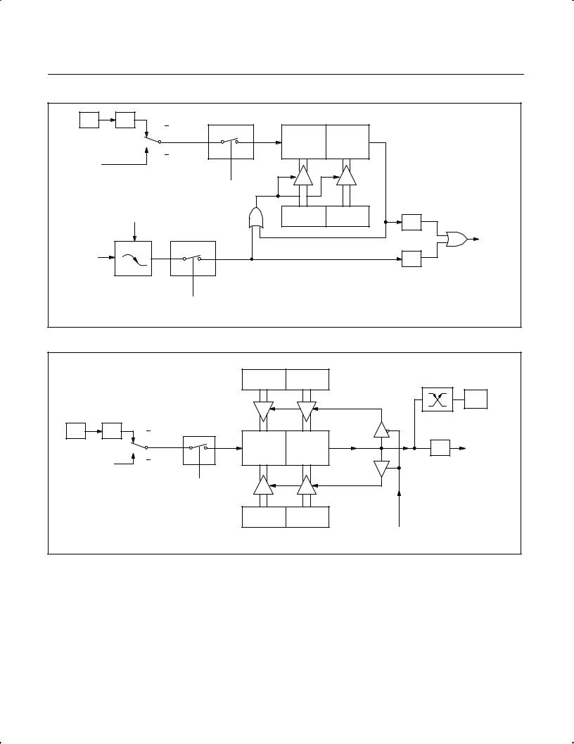
Philips Semiconductors |
Product data |
|
|
|
|
80C51 8-bit Flash microcontroller family |
|
P89C51RB2/P89C51RC2/ |
||
16KB/32KB/64KB ISP/IAP Flash with 512B/512B/1KB RAM |
P89C51RD2Hxx |
|||
OSC |
n* |
|
|
|
|
C/T2 = 0 |
|
|
|
|
|
|
TL2 |
TH2 |
|
|
|
(8 BITS) |
(8 BITS) |
|
C/T2 = 1 |
|
|
|
T2 PIN |
|
CONTROL |
|
|
|
|
|
|
|
|
TR2 |
RELOAD |
|
|
|
|
|
|
|
|
TRANSITION |
|
|
|
|
DETECTOR |
|
RCAP2L |
RCAP2H |
|
|
|
|
TF2 |
|
|
|
|
TIMER 2 |
|
|
|
|
INTERRUPT |
T2EX PIN |
|
|
|
EXF2 |
|
CONTROL |
|
|
|
|
EXEN2 |
|
|
SU01253 |
* n = 6 in 6-clock mode, or 12 in 12-clock mode. |
|
|
|
|
Figure 4. Timer 2 in Auto-Reload Mode (DCEN = 0)
|
|
(DOWN COUNTING RELOAD VALUE) |
|
|
|
|
|
FFH |
FFH |
TOGGLE |
|
|
|
|
|
|
|
|
|
|
|
|
EXF2 |
OSC |
n* |
C/T2 = 0 |
|
|
|
|
|
|
|
OVERFLOW |
|
|
|
TL2 |
TH2 |
TF2 |
INTERRUPT |
|
T2 PIN |
C/T2 = 1 |
|
|
|
|
|
CONTROL |
|
|
|
|
|
TR2 |
|
COUNT |
|
|
|
|
|
|
|
|
|
|
|
DIRECTION |
|
|
|
|
|
1 = UP |
|
|
|
|
|
0 = DOWN |
|
|
|
RCAP2L |
RCAP2H |
|
|
|
|
(UP COUNTING RELOAD VALUE) |
T2EX PIN |
|
|
* n = 6 in 6-clock mode, or 12 in 12-clock mode. |
|
|
SU01254 |
||
Figure 5. Timer 2 Auto Reload Mode (DCEN = 1)
2002 May 24 |
12 |
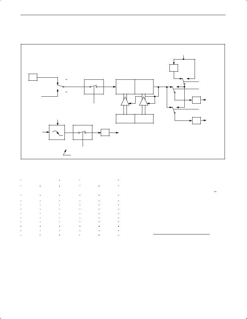
Philips Semiconductors Product data
80C51 8-bit Flash microcontroller family |
P89C51RB2/P89C51RC2/ |
16KB/32KB/64KB ISP/IAP Flash with 512B/512B/1KB RAM |
P89C51RD2Hxx |
|
|
Timer 1
Overflow
|
|
|
|
2 |
|
|
|
OSC |
|
|
|
|
ª0º |
ª1º |
|
|
|
|
|
|
|
|
|
|
C/T2 = 0 |
|
|
|
|
|
SMOD |
|
|
|
|
ª1º |
ª0º |
|
|
|
|
TL2 |
TH2 |
|
|
||
|
|
|
|
|
|
||
|
|
(8-bits) |
(8-bits) |
|
|
|
RCLK |
|
C/T2 = 1 |
|
|
|
|
|
|
T2 Pin |
Control |
|
|
|
|
|
|
|
|
|
|
|
16 |
|
|
|
|
|
|
|
|
RX Clock |
|
|
TR2 |
|
Reload |
ª1º |
ª0º |
|
|
|
|
|
|
|
TCLK |
||
|
|
|
|
|
|
||
|
|
|
|
|
|
|
|
|
Transition |
|
|
|
|
|
|
|
Detector |
RCAP2L |
RCAP2H |
|
|
16 |
|
|
|
|
|
TX Clock |
|||
|
|
|
|
|
|
||
T2EX Pin |
EXF2 |
Timer 2 |
|
|
|
|
|
|
|
Interrupt |
|
|
|
|
|
Control
EXEN2
Note availability of additional external interrupt.
SU01213
Figure 6. Timer 2 in Baud Rate Generator Mode
Table 3. Timer 2 Generated Commonly Used
Baud Rates
Baud Rate |
|
Timer 2 |
|||
|
|
Osc Freq |
|
|
|
12 clock |
6 clock |
RCAP2H |
RCAP2L |
||
|
|||||
mode |
mode |
|
|||
|
|
|
|||
|
|
|
|
|
|
375 k |
750 k |
12 MHz |
FF |
FF |
|
9.6 k |
19.2 k |
12 MHz |
FF |
D9 |
|
2.8 k |
5.6 k |
12 MHz |
FF |
B2 |
|
2.4 k |
4.8 k |
12 MHz |
FF |
64 |
|
1.2 k |
2.4 k |
12 MHz |
FE |
C8 |
|
300 |
600 |
12 MHz |
FB |
1E |
|
110 |
220 |
12 MHz |
F2 |
AF |
|
300 |
600 |
6 MHz |
FD |
8F |
|
110 |
220 |
6 MHz |
F9 |
57 |
|
|
|
|
|
|
|
The baud rates in modes 1 and 3 are determined by Timer 2's overflow rate given below:
Modes 1 and 3 Baud Rates + Timer 2 Overflow Rate 16
The timer can be configured for either ªtimerº or ªcounterº operation. In many applications, it is configured for ªtimerº operation (C/T2*=0). Timer operation is different for Timer 2 when it is being used as a baud rate generator.
Usually, as a timer it would increment every machine cycle (i.e.,
1/6 the oscillator frequency in 6 clock mode, 1/12 the oscillator frequency in 12 clock mode). As a baud rate generator, it increments at the oscillator frequency in 6 clock mode (OSC/2 in 12 clock mode). Thus the baud rate formula is as follows:
Modes 1 and 3 Baud Rates =
Oscillator Frequency
[ n * [65536 (RCAP2H, RCAP2L)]]
Baud Rate Generator Mode
Bits TCLK and/or RCLK in T2CON (Table 3) allow the serial port transmit and receive baud rates to be derived from either Timer 1 or Timer 2. When TCLK= 0, Timer 1 is used as the serial port transmit baud rate generator. When TCLK= 1, Timer 2 is used as the serial port transmit baud rate generator. RCLK has the same effect for the serial port receive baud rate. With these two bits, the serial port can have different receive and transmit baud rates ± one generated by Timer 1, the other by Timer 2.
Figure 6 shows the Timer 2 in baud rate generation mode. The baud rate generation mode is like the auto-reload mode,in that a rollover in
TH2 causes the Timer 2 registers to be reloaded with the 16-bit value in registers RCAP2H and RCAP2L, which are preset by software.
* n = |
16 in 6 clock mode |
|
32 in 12 clock mode |
Where: (RCAP2H, RCAP2L)= The content of RCAP2H and
RCAP2L taken as a 16-bit unsigned integer.
The Timer 2 as a baud rate generator mode shown in Figure 6, is valid only if RCLK and/or TCLK = 1 in T2CON register. Note that a rollover in TH2 does not set TF2, and will not generate an interrupt.
Thus, the Timer 2 interrupt does not have to be disabled when Timer 2 is in the baud rate generator mode. Also if the EXEN2
(T2 external enable flag) is set, a 1-to-0 transition in T2EX
(Timer/counter 2 trigger input) will set EXF2 (T2 external flag) but will not cause a reload from (RCAP2H, RCAP2L) to (TH2,TL2).
Therefore when Timer 2 is in use as a baud rate generator, T2EX can be used as an additional external interrupt, if needed.
2002 May 24 |
13 |

Philips Semiconductors Product data
80C51 8-bit Flash microcontroller family |
P89C51RB2/P89C51RC2/ |
16KB/32KB/64KB ISP/IAP Flash with 512B/512B/1KB RAM |
P89C51RD2Hxx |
|
|
When Timer 2 is in the baud rate generator mode, one should not try to read or write TH2 and TL2. As a baud rate generator, Timer 2 is incremented every state time (osc/2) or asynchronously from pin T2; under these conditions, a read or write of TH2 or TL2 may not be accurate. The RCAP2 registers may be read, but should not be written to, because a write might overlap a reload and cause write and/or reload errors. The timer should be turned off (clear TR2) before accessing the Timer 2 or RCAP2 registers.
Table 3 shows commonly used baud rates and how they can be obtained from Timer 2.
Summary of Baud Rate Equations
Timer 2 is in baud rate generating mode. If Timer 2 is being clocked through pin T2(P1.0) the baud rate is:
Baud Rate + Timer 2 Overflow Rate
16
If Timer 2 is being clocked internally, the baud rate is:
Baud Rate + |
|
|
fOSC |
[ n * |
[65536 (RCAP2H, RCAP2L)]] |
||
|
* n = |
16 in |
6 clock mode |
|
|
32 in |
12 clock mode |
Where fOSC= Oscillator Frequency
To obtain the reload value for RCAP2H and RCAP2L, the above equation can be rewritten as:
RCAP2H, RCAP2L + 65536 |
|
fOSC |
|
|
|
n * |
Baud Rate |
|
|
Timer/Counter 2 Set-up
Except for the baud rate generator mode, the values given for T2CON do not include the setting of the TR2 bit. Therefore, bit TR2 must be set, separately, to turn the timer on. see Table 4 for set-up of Timer 2 as a timer. Also see Table 5 for set-up of Timer 2 as a counter.
Table 4. Timer 2 as a Timer
|
|
T2CON |
|
MODE |
|
|
|
INTERNAL CONTROL |
|
EXTERNAL CONTROL |
|
|
|
||
|
(Note 1) |
|
(Note 2) |
|
|
|
|
16-bit Auto-Reload |
00H |
|
08H |
|
|
|
|
16-bit Capture |
01H |
|
09H |
|
|
|
|
Baud rate generator receive and transmit same baud rate |
34H |
|
36H |
|
|
|
|
Receive only |
24H |
|
26H |
|
|
|
|
Transmit only |
14H |
|
16H |
|
|
|
|
Table 5. Timer 2 as a Counter
|
|
|
TMOD |
|
|
MODE |
|
|
|
|
INTERNAL CONTROL |
|
EXTERNAL CONTROL |
|
|
|
|
||
|
|
(Note 1) |
|
(Note 2) |
|
|
|
|
|
16-bit |
|
02H |
|
0AH |
|
|
|
|
|
Auto-Reload |
|
03H |
|
0BH |
|
|
|
|
|
NOTES:
1.Capture/reload occurs only on timer/counter overflow.
2.Capture/reload occurs on timer/counter overflow and a 1-to-0 transition on T2EX (P1.1) pin except when Timer 2 is used in the baud rate generator mode.
2002 May 24 |
14 |
 Loading...