


PCF8584U-10

DATA SH EET
Product specification
Supersedes data of 1997 Mar 19
File under Integrated Circuits, IC12
1997 Oct 21
INTEGRATED CIRCUITS
PCF8584
I
2
C-bus controller

1997 Oct 21 2
Philips Semiconductors Product specification
I2C-bus controller
PCF8584
CONTENTS
1 FEATURES
2 GENERAL DESCRIPTION
3 ORDERING INFORMATION
4 BLOCK DIAGRAM
5 PINNING
6 FUNCTIONAL DESCRIPTION
6.1 General
6.2 Interface Mode Control (IMC)
6.3 Set-up registers S0', S2 and S3
6.4 Own address register S0'
6.5 Clock register S2
6.6 Interrupt vector S3
6.7 Data shift register/read buffer S0
6.8 Control/status register S1
6.8.1 Register S1 control section
6.8.1.1 PIN (Pending Interrupt Not)
6.8.1.2 ESO (Enable Serial Output)
6.8.1.3 ES1 and ES2
6.8.1.4 ENI
6.8.1.5 STA and STO
6.8.1.6 ACK
6.8.2 Register S1 status section
6.8.2.1 PIN bit
6.8.2.2 STS
6.8.2.3 BER
6.8.2.4 LRB/AD0
6.8.2.5 AAS
6.8.2.6 LAB
6.8.2.7 BB
6.9 Multi-master operation
6.10 Reset
6.11 Comparison to the MAB8400 I2C-bus interface
6.11.1 Deleted functions
6.11.2 added functions
6.12 Special function modes
6.12.1 Strobe
6.12.2 Long-distance mode
6.12.3 Monitor mode
7 SOFTWARE FLOWCHART EXAMPLES
7.1 Initialization
7.2 Implementation
8I
2
C-BUS TIMING DIAGRAMS
9 LIMITING VALUES
10 HANDLING
11 DC CHARACTERISTICS
12 I2C-BUS TIMING SPECIFICATIONS
13 PARALLEL INTERFACE TIMING
14 APPLICATION INFORMATION
14.1 Application Notes
15 PACKAGE OUTLINES
16 SOLDERING
16.1 Introduction
16.2 DIP
16.2.1 Soldering by dipping or by wave
16.2.2 Repairing soldered joints
16.3 SO
16.3.1 Reflow soldering
16.3.2 Wave soldering
16.3.3 Repairing soldered joints
17 DEFINITIONS
18 LIFE SUPPORT APPLICATIONS
19 PURCHASE OF PHILIPS I2C COMPONENTS
1997 Oct 21 3
Philips Semiconductors Product specification
I2C-bus controller
PCF8584
1 FEATURES
• Parallel-bus to I2C-bus protocol converter and interface
• Compatible with most parallel-bus
microcontrollers/microprocessors including 8049, 8051,
6800, 68000 and Z80
• Both master and slave functions
• Automatic detection and adaption to bus interface type
• Programmable interrupt vector
• Multi-master capability
• I2C-bus monitor mode
• Long-distance mode (4-wire)
• Operating supply voltage 4.5 to 5.5 V
• Operating temperature range: −40 to +85 °C.
2 GENERAL DESCRIPTION
The PCF8584 is an integrated circuit designed in CMOS
technology which serves as an interface between most
standard parallel-bus microcontrollers/microprocessors
and the serial I2C-bus. The PCF8584 provides both master
and slave functions.
Communication with the I2C-bus is carried out on a
byte-wise basis using interrupt or polled handshake.
It controls all the I2C-bus specific sequences, protocol,
arbitration and timing. The PCF8584 allows parallel-bus
systems to communicate bidirectionally with the I
2
C-bus.
3 ORDERING INFORMATION
TYPE
NUMBER
PACKAGE
NAME DESCRIPTION VERSION
PCF8584P DIP20 plastic dual in-line package; 20 leads (300 mil) SOT146-1
PCF8584T SO20 plastic small outline package; 20 leads; body width 7.5 mm SOT163-1
1997 Oct 21 4
Philips Semiconductors Product specification
I2C-bus controller
PCF8584
4 BLOCK DIAGRAM
Fig.1 Block diagram.
(1) X = don’t care.
(2) Pin mnemonics between parenthesis indicate the 68000 mode pin designations.
(3) These pin mnemonics represent the long-distance mode pin designations.
handbook, full pagewidth
MBD908 - 1
DB6DB7 DB5 DB4 DB3 DB2 DB1 DB0
1415 13 12 11 9 8 7
READ BUFFER
SHIFT REGISTER
DATA SHIFT REGISTER S0 AND READ BUFFER
write
only
8
MSB
MSB LSB
COMPARATOR S0, S0'
OWN ADDRESS S0'
X
8
INTERRUPT VECTOR S3
8
CLOCK REGISTER S2
8
S20S21S22S23S24000
CLOCK REGISTER S2
8
ACKSTOSTAENIES2ES1ES0PIN
REGISTER S1
CONTROL STATUS
BBLABAAS
AD0/
LRB
BERSTS0PIN
write only
read only
REGISTER ACCESS CONTROL
BUS BUFFER CONTROL
INTERRUPT CONTROL
RESET/STROBE CONTROL
INT
SCL OUT
IACK
SDA IN
CLK
541
VV
DD SS
20 10
DATA CONTROL
DIGITAL
FILTER
SDA/
SDA OUT
2
SCL CONTROL
DIGITAL
FILTER
SCL/
SCL IN
3
PCF8584
RESET/ CS A0
19 17 6
STROBE
(O.C.)
WR (R/W)18RD (DTACK)
16
CLOCK PRESCALER
SCL MULTIPLEXER
BUS BUSY LOGIC
ARBITRATION LOGIC
X
PARALLEL BUS
CONTROL STATUS REGISTER S1
read
only
(1)
(1)
(3)
(3)
(2) (2)
(3) (3)
PARALLEL BUS CONTROL
default: 00H 80XX
0FH 68XXX

1997 Oct 21 5
Philips Semiconductors Product specification
I2C-bus controller
PCF8584
5 PINNING
SYMBOL PIN I/O DESCRIPTION
CLK 1 I clock input from microcontroller clock generator (internal pull-up)
SDA or
SDA OUT
2 I/O I2C-bus serial data input/output (open-drain). Serial data output in long-distance
mode.
SCL or SCL IN 3 I/O I
2
C-serial clock input/output (open-drain). Serial clock input in long-distance mode.
IACK or
SDA IN
4 I Interrupt acknowledge input (internal pull-up); when this signal is asserted the
interrupt vector in register S3 will be available at the bus Port if the ENI flag is set.
Serial data input in long-distance mode.
INT or
SCL OUT
5 O Interrupt output (open-drain); this signal is enabled by the ENI flag in register S1.
It is asserted when the PIN flag is reset. (PIN is reset after 1 byte is transmitted or
received over the I2C-bus). Serial clock output in long-distance mode.
A0 6 I Register select input (internal pull-up); this input selects between the control/status
register and the other registers. Logic 1 selects register S1, logic 0 selects one of
the other registers depending on bits loaded in ESO, ES1 and ES2 of register S1.
DB0 7 I/O bidirectional 8-bit bus Port 0
DB1 8 I/O bidirectional 8-bit bus Port 1
DB2 9 I/O bidirectional 8-bit bus Port 2
V
SS
10 − ground
DB3 11 I/O bidirectional 8-bit bus Port 3
DB4 12 I/O bidirectional 8-bit bus Port 4
DB5 13 I/O bidirectional 8-bit bus Port 5
DB6 14 I/O bidirectional 8-bit bus Port 6
DB7 15 I/O bidirectional 8-bit bus Port 7
RD (DTACK) 16 I/(O) RD is the read control input for MAB8049, MAB8051 or Z80-types. DTACK is the
data transfer control output for 68000-types (open-drain).
CS 17 I chip select input (internal pull-up)
WR (R/W) 18 I WR is the write control input for MAB8048, MAB8051, or Z80-types
(internal pull-up). R/W control input for 68000-types.
RESET/
STROBE
19 I/O Reset input (open-drain); this input forces the I2C-bus controller into a predefined
state; all flags are reset, except PIN, which is set. Also functions as strobe output.
V
DD
20 − supply voltage

1997 Oct 21 6
Philips Semiconductors Product specification
I2C-bus controller
PCF8584
6 FUNCTIONAL DESCRIPTION
6.1 General
The PCF8584 acts as an interface device between
standard high-speed parallel buses and the serial I
2
C-bus.
On the I2C-bus, it can act either as master or slave.
Bidirectional data transfer between the I2C-bus and the
parallel-bus microcontroller is carried out on a byte-wise
basis, using either an interrupt or polled handshake.
Interface to either 80XX-type (e.g. 8048, 8051, Z80) or
68000-type buses is possible. Selection of bus type is
automatically performed (see Section 6.2).
Fig.2 Pin configuration.
handbook, halfpage
CLK
SDA or SDA OUT
SCL or SCL IN
A0
DB0
DB1
DB2
V
SS
V
DD
DB7
DB6
DB5
DB4
DB3
1
2
3
4
5
6
7
8
9
10
20
19
18
17
16
15
14
13
12
11
PCF8584
MLA012 - 1
IACK or SDA IN
INT or SCL OUT
RESET / STROBE
CS
RD (DTACK)
WR (R/W)
(1)
(1)
(1) Pin mnemonics between parenthesis indicate the 68000 mode
pin designations.
Table 1 Control signals utilized by the PCF8584 for
microcontroller/microprocessor interfacing
The structure of the PCF8584 is similar to that of the
I
2
C-bus interface section of the Philips’
MABXXXX/PCF84(C)XX-series of microcontrollers, but
with a modified control structure. The PCF8584 has five
internal register locations. Three of these (own address
register S0', clock register S2 and interrupt vector S3) are
used for initialization of the PCF8584. Normally they are
only written once directly after resetting of the PCF8584.
The remaining two registers function as double registers
(data buffer/shift register S0, and control/status
register S1) which are used during actual data
transmission/reception. By using these double registers,
which are separately write and read accessible, overhead
for register access is reduced. Register S0 is a
combination of a shift register and data buffer.
Register S0 performs all serial-to-parallel interfacing with
the I2C-bus.
Register S1 contains I2C-bus status information required
for bus access and/or monitoring.
6.2 Interface Mode Control (IMC)
Selection of either an 80XX mode or 68000 mode
interface is achieved by detection of the first
WR-CS signal
sequence. The concept takes advantage of the fact that
the write control input is common for both types of
interfaces. An 80XX-type interface is default. If a
HIGH-to-LOW transition ofWR (R/W) is detected while CS
is HIGH, the 68000-type interface mode is selected and
theDTACK output is enabled. Care must be taken thatWR
and CS are stable after reset.
TYPE R/
W WR R DTACK IACK
8048/
8051
no yes yes no no
68000 yes no no yes yes
Z80 no yes yes no yes
1997 Oct 21 7
Philips Semiconductors Product specification
I2C-bus controller
PCF8584
Fig.3 68000/80XX timing sequence utilized by the Interface Mode Control (IMC).
handbook, full pagewidth
FILTER
t = 16CLK
RESET
STROBE
D
EN
D
EN
ENRD
SIO DIVIDER
(S21 and S20)
DIVIDER
(S24, S23, S22)
/2, 3, 4, 5, 8
I2C-bus
(1.5 MHz)
CS A0
SCL
INT IACK CLK
(50 : 50)
WR/
R/W
RD/
DTACK
MBE706
handbook, full pagewidth
mode select
mode locked
R/W
CS
DTACK
mode select
WR
CS
MBE707
(1)
(2)
(1) Bus timing; 68000 mode write cycle.
(2) Bus timing; 80XX mode.
1997 Oct 21 8
Philips Semiconductors Product specification
I2C-bus controller
PCF8584
6.3 Set-up registers S0', S2 and S3
Registers S0', S2 and S3 are used for initialization of the
PCF8584 (see Fig.5 ‘Initialization sequence’ flowchart).
6.4 Own address register S0'
When the PCF8584 is addressed as slave, this register
must be loaded with the 7-bit I
2
C-bus address to which the
PCF8584 is to respond. During initialization, the own
address register S0' must be written to, regardless
whether it is later used. The Addressed As Slave (AAS) bit
in status register S1 is set when this address is received
(the value in S0 is compared with the value in S0'). Note
that the S0 and S0' registers are offset by one bit; hence,
programming the own address register S0' with a value of
55H will result in the value AAH being recognized as the
PCF8584’s slave address (see Fig.1).
Programming of S0' is accomplished via the parallel-bus
when A0 is LOW, with the appropriate bit combinations set
in control status register S1 (S1 is written when
pin A0 = HIGH). Bit combinations for accessing all
registers are given in Table 5. After reset, S0' has default
address 00H (PCF8584 is thus initially in monitor mode,
see Section 6.12.3).
6.5 Clock register S2
Register S2 provides control over chip clock frequency
and SCL clock frequency. S20 and S21 provide a selection
of 4 different I
2
C-bus SCL frequencies which are shown in
Table 2. Note that these SCL frequencies are only
obtained when bits S24, S23 and S22 are programmed to
the correct input clock frequency (f
clk
).
Table 2 Register S2 selection of SCL frequency
S22, S23 and S24 are used for control of the internal clock
prescaler. Due to the possibility of varying microcontroller
clock signals, the prescaler can be programmed to adapt
to 5 different clock rates, thus providing a constant internal
clock. This is required to provide a stable time base for the
SCL generator and the digital filters associated with the
I
2
C-bus signals SCL and SDA. Selection for adaption to
external clock rates is shown in Table 3.
BIT
APPROXIMATE SCL
FREQUENCY f
SCL
(kHz)
S21 S20
00 90
01 45
10 11
1 1 1.5
Programming of S2 is accomplished via the parallel-bus
when A0 = LOW, with the appropriate bit combinations set
in control status register S1 (S1 is written when
A0 = HIGH). Bit combinations for accessing all registers
are given in Table 5.
Table 3 Register S2 selection of clock frequency
Note
1. X = don’t care.
6.6 Interrupt vector S3
The interrupt vector register provides an 8-bit
user-programmable vector for vectored-interrupt
microcontrollers. The vector is sent to the bus port
(DB7 to DB0) when an interrupt acknowledge signal is
asserted and the ENI (enable interrupt) flag is set. Default
vector values are:
• Vector is ‘00H’ in 80XX mode
• Vector is ‘0FH’ in 68000 mode.
On reset the PCF8584 is in the 80XX mode, thus the
default interrupt vector is ‘00H’.
6.7 Data shift register/read buffer S0
Register S0 acts as serial shift register and read buffer
interfacing to the I
2
C-bus. All read and write operations
to/from the I2C-bus are done via this register. S0 is a
combination of a shift register and a data buffer; parallel
data is always written to the shift register, and read from
the data buffer. I2C-bus data is always shifted in or out of
shift register S0.
INTERNAL CLOCK FREQUENCY
S24 S23 S22 f
clk
(MHz)
0X
(1)
X
(1)
3
1 0 0 4.43
1016
1108
11112
1997 Oct 21 9
Philips Semiconductors Product specification
I2C-bus controller
PCF8584
In receiver mode the data from the shift register is copied to the read buffer during the acknowledge phase. Further
reception of data is inhibited (SCL held LOW) until the S0 read buffer is read (see Section 6.8.1.1).
In the transmitter mode data is transmitted to the I2C-bus as soon as it is written to the S0 shift register if the serial I/O is
enabled (ESO = 1).
Remarks:
1. A minimum of 6 clock cycles must elapse between consecutive parallel-bus accesses to the PCF8584 when the
I2C-bus controller operates at 8 or 12 MHz. This may be reduced to 3 clock cycles for lower operating frequencies.
2. To start a read operation immediately after a write, it is necessary to read the S0 read buffer in order to invoke
reception of the first byte (‘dummy read’ of the address). Immediately after the acknowledgement, this first byte will
be transferred from the shift register to the read buffer. The next read will then transfer the correct value of the first
byte to the microcontroller bus (see Fig.7).
6.8 Control/status register S1
Register S1 controls I
2
C-bus operation and provides I2C-bus status information. Register S1 is accessed by a HIGH
signal on register select input A0. For more efficient communication between microcontroller/processor and the I2C-bus,
register S1 has separate read and write functions for all bit positions (see Fig.3). The write-only section provides register
access control and control over I2C-bus signals, while the read-only section provides I2C-bus status information.
Table 4 Control/status register S1
Notes
1. For further information see Section 6.8.1.
2. For further information see Section 6.8.2.
3. Logic 1 if not-initialized.
CONTROL/STATUS BITS MODE
Control
(1)
PIN ESO ES1 ES2 ENI STA STO ACK write only
Status
(2)
PIN 0
(3)
STS BER AD0/LRB AAS LAB BB read only
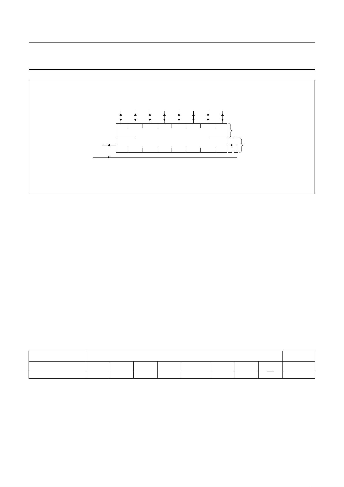
Fig.4 Data shift register/bus buffer S0.
ndbook, full pagewidth
DB7 DB6 DB5 DB4 DB3 DB2 DB1 DB0
Read Buffer
Data Shift Register S0 and Read Buffer
Shift register
Read
only
Write
only
to/from
I
2
C-Bus SDA line
to/from microcontroller parallel bus
MBE705
1997 Oct 21 10
Philips Semiconductors Product specification
I2C-bus controller
PCF8584
6.8.1 REGISTER S1 CONTROL SECTION
The write-only section of S1 enables access to registers S0, S0', S1, S2 and S3, and controls I2C-bus operation; see
Table 4.
6.8.1.1 PIN (Pending Interrupt Not)
When the PIN bit is written with a logic 1, all status bits are reset to logic 0. This may serve as a software reset function
(see Figs 5 to 9). PIN is the only bit in S1 which may be both read and written to. PIN is mostly used as a status bit for
synchronizing serial communication, see Section 6.8.2.
6.8.1.2 ESO (Enable Serial Output)
ESO enables or disables the serial I2C-bus I/O. When ESO is LOW, register access for initialization is possible. When
ESO is HIGH, I2C-bus communication is enabled; communication with serial shift register S0 is enabled and the S1 bus
status bits are made available for reading.
Table 5 Register access control; ESO = 0 (serial interface off) and ESO = 1 (serial interface on)
Notes
1. With ESO = 0, bits ENI, STA, STO and ACK of S1 can be read for test purposes.
2. ‘X’ if ENI = 0.
6.8.1.3 ES1 and ES2
ES1 and ES2 control selection of other registers for initialization and control of normal operation. After these bits are
programmed for access to the desired register (shown in Table 5), the register is selected by a logic LOW level on
register select pin A0.
6.8.1.4 ENI
This bit enables the external interrupt output INT, which is generated when the PIN bit is active (logic 0).
This bit must be set to logic 0 before entering the long-distance mode, and remain at logic 0 during operation in
long-distance mode.
INTERNAL REGISTER ADDRESSING 2-WIRE MODE
A0 ES1 ES2
IACK FUNCTION
ESO = 0; serial interface off (see note 1)
10X1
(2)
R/W S1: control
0001
(2)
R/W S0': (own address)
0011
(2)
R/W S3: (interrupt vector)
0101
(2)
R/W S2: (clock register)
ESO = 1; serial interface on
1 0 X 1 W S1: control
1 0 X 1 R S1; status
0001R/WS0: (data)
0011R/WS3: (interrupt vector)
X 0 X 0 R S3: (interrupt vector ACK cycle))
1997 Oct 21 11
Philips Semiconductors Product specification
I2C-bus controller
PCF8584
6.8.1.5 STA and STO
These bits control the generation of the I2C-bus START condition and transmission of slave address and R/W bit,
generation of repeated START condition, and generation of the STOP condition (see Table 7).
Table 6 Register access control; ESO = 1 (serial interface on) and ES1 = 1; long-distance (4-wire) mode; note 1
Note
1. Trying to read from or write to registers other than S0 and S1 (setting ESO = 0) brings the PCF8584 out of the
long-distance mode.
Table 7 Instruction table for serial bus control
Notes
1. In master receiver mode, the last byte must be terminated with ACK bit HIGH (‘negative acknowledge’).
2. If both STA and STO are set HIGH simultaneously in master mode, a STOP condition followed by a START
condition + address will be generated. This allows ‘chaining’ of transmissions without relinquishing bus control.
3. All other STA and STO mode combinations not mentioned in Table 7 are NOPs.
6.8.1.6 ACK
This bit must be set normally to a logic 1. This causes the I2C-bus controller to send an acknowledge automatically after
each byte (this occurs during the 9th clock pulse). The bit must be reset (to logic 0) when the I2C-bus controller is
operating in master/receiver mode and requires no further data to be sent from the slave transmitter. This causes a
negative acknowledge on the I2C-bus, which halts further transmission from the slave device.
6.8.2 R
EGISTER S1 STATUS SECTION
The read-only section of S1 enables access to I2C-bus status information; see Table 4.
INTERNAL REGISTER ADDRESSING: LONG-DISTANCE (4-WIRE) MODE
A0 ES1 ES2
IACK FUNCTION
1 1 X 1 W S1: control
1 1 X X R S1; status
0 1 X X R/W S0; (data)
STA STO
PRESENT
MODE
FUNCTION OPERATION
1 0 SLV/REC START transmit START + address, remain
MST/TRM if R/
W=0;
go to MST/REC if R/W=1
1 0 MST/TRM REPEAT
START
same as for SLV/REC
0 1 MST/REC;
MST/TRM
STOP READ;
STOP WRITE
transmit STOP go to SLV/REC mode; note 1
1 1 MST DATA
CHAINING
send STOP, START and address after last
master frame without STOP sent; note 2
0 0 ANY NOP no operation; note 3

1997 Oct 21 12
Philips Semiconductors Product specification
I2C-bus controller
PCF8584
6.8.2.1 PIN bit
‘Pending Interrupt Not’ (MSB of register S1) is a status flag
which is used to synchronize serial communication and is
set to logic 0 whenever the PCF8584 requires servicing.
The PIN bit is normally read in polled applications to
determine when an I2C-bus byte transmission/reception is
completed. The PIN bit may also be written, see
Section 6.8.1.
Each time a serial data transmission is initiated (by setting
the STA bit in the same register), the PIN bit will be set to
logic 1 automatically (inactive). When acting as
transmitter, PIN is also set to logic 1 (inactive) each time
S0 is written. In receiver mode, the PIN bit is automatically
set to logic 1 (inactive) each time the data register S0 is
read.
After transmission or reception of one byte on the I
2
C-bus
(9 clock pulses, including acknowledge), the PIN bit will be
automatically reset to logic 0 (active) indicating a complete
byte transmission/reception. When the PIN bit is
subsequently set to logic 1 (inactive), all status bits will be
reset to logic 0. PIN is also set to zero on a BER (bus error)
condition.
In polled applications, the PIN bit is tested to determine
when a serial transmission/reception has been completed.
When the ENI bit (bit 4 of write-only section of register S1)
is also set to logic 1 the hardware interrupt is enabled.
In this case, the PIN flag also triggers an external interrupt
(active LOW) via the INT output each time PIN is reset to
logic 0 (active).
When acting as slave transmitter or slave receiver, while
PIN = 0, the PCF8584 will suspend I2C-bus transmission
by holding the SCL line LOW until the PIN bit is set to
logic 1 (inactive). This prevents further data from being
transmitted or received until the current data byte in S0 has
been read (when acting as slave receiver) or the next data
byte is written to S0 (when acting as slave transmitter).
PIN bit summary:
• The PIN bit can be used in polled applications to test
when a serial transmission has been completed. When
the ENI bit is also set, the PIN flag sets the external
interrupt via the INT output.
• Setting the STA bit (start bit) will set PIN = 1 (inactive).
• In transmitter mode, after successful transmission of
one byte on the I2C-bus the PIN bit will be automatically
reset to logic 0 (active) indicating a complete byte
transmission.
• In transmitter mode, PIN is set to logic 1 (inactive) each
time register S0 is written.
• In receiver mode, PIN is set to logic 0 (active) on
completion of each received byte. Subsequently, the
SCL line will be held LOW until PIN is set to logic 1.
• In receiver mode, when register S0 is read, PIN is set to
logic 1 (inactive).
• In slave receiver mode, an I
2
C-bus STOP condition will
set PIN = 0 (active).
• PIN = 0 if a bus error (BER) occurs.
6.8.2.2 STS
When in slave receiver mode, this flag is asserted when an
externally generated STOP condition is detected (used
only in slave receiver mode).
6.8.2.3 BER
Bus error; a misplaced START or STOP condition has
been detected. Resets BB (to logic 1; inactive), sets
PIN = 0 (active).
6.8.2.4 LRB/AD0
‘Last Received Bit’ or ‘Address 0 (General Call) bit’. This
status bit serves a dual function, and is valid only while
PIN = 0:
1. LRB holds the value of the last received bit over the
I2C-bus while AAS = 0 (not addressed as slave).
Normally this will be the value of the slave
acknowledgement; thus checking for slave
acknowledgement is done via testing of the LRB.
2. AD0; when AAS = 1 (‘Addressed As Slave’ condition),
the I2C-bus controller has been addressed as a slave.
Under this condition, this bit becomes the ‘AD0’ bit and
will be set to logic 1 if the slave address received was
the ‘general call’ (00H) address, or logic 0 if it was the
I2C-bus controller’s own slave address.
6.8.2.5 AAS
‘Addressed As Slave’ bit. Valid only when PIN = 0. When
acting as slave receiver, this flag is set when an incoming
address over the I2C-bus matches the value in own
address register S0' (shifted by one bit, see Section 6.4),
or if the I2C-bus ‘General Call’ address (00H) has been
received (‘General Call’ is indicated when AD0 status bit is
also set to logic 1, see Section 6.8.2.4).
6.8.2.6 LAB
‘Lost Arbitration’ Bit. This bit is set when, in multi-master
operation, arbitration is lost to another master on the
I2C-bus.
 Loading...