


PCF1175CT-F2

DATA SH EET
Product specification
Supersedes data of September 1993
File under Integrated Circuits, IC16
1997 Apr 16
INTEGRATED CIRCUITS
PCF1175C
4-digit duplex LCD car clock
1997 Apr 16 2
Philips Semiconductors Product specification
4-digit duplex LCD car clock PCF1175C
FEATURES
• Internal voltage regulator is electrically programmable
for various LCD voltages
• Time calibration is electrically programmable
(no trimming capacitor required)
• LCD voltage adjusts with temperature for good contrast
• 4.19 MHz oscillator
• 12-hour or 24-hour mode
• Operating ambient temperature: −40 to +85 °C
• 28-lead plastic SMD (SO28)
• 1 Hz set mode.
GENERAL DESCRIPTION
The PCF1175C is a single chip, 4.19 MHz CMOS car clock
circuit providing hours, minutes and seconds functions.
It is designed to drive a 4-digit duplex liquid crystal display
(LCD).
Two external single-pole, single-throw switches will
accomplish all time setting functions. Time calibration and
voltage regulator are electrically programmable via an
on-chip EEPROM. The circuit is battery-operated via an
internal voltage regulator and an external resistor.
ORDERING INFORMATION
Notes
1. See Fig.1 and Chapter “Package outline” for pin layout and package details.
2. See Chapter “Chip dimensions and bonding pad locations” for pad layout and package details.
TYPE
NUMBER
PACKAGE
NAME DESCRIPTION VERSION
PCF1175CT SO28 plastic small outline package; 28 leads; body width 7.5 mm
(1)
SOT136-1
PCF1175CU − uncased chip in tray
(2)
−
PCF1175CU/10 − chip-on-film frame carrier (FFC)
(2)
−

1997 Apr 16 3
Philips Semiconductors Product specification
4-digit duplex LCD car clock PCF1175C
PINNING
SYMBOL PIN DESCRIPTION
S1 1 hour adjustment input
DATA 2 EEPROM data input
OSC IN 3 oscillator input
OSC OUT 4 oscillator output
V
SS
5 negative supply voltage
MODE 6 12/24-hour mode select input
V
PP
7 programming voltage input
TS 8 test speed-up mode input
ENABLE 9 enable input (for S1 and S2)
V
DD
10 positive supply voltage
FLASH 11 colon option input
SEL 12 EEPROM select input
S2 13 minute adjustment input
B4/C4 14 segment driver
G4/D4 15 segment driver
F4/E4 16 segment driver
B3/C3 17 segment driver
G3/AD3 18 segment driver
F3/E3 19 segment driver
A4/COL 20 segment driver
B2/C2 21 segment driver
G2/D2 22 segment driver
F2/E2 23 segment driver
B1/C1 24 segment driver
A2/ADEG1 25 segment driver
AM/PM 26 segment driver
BP2 27 backplane 2
BP1 28 backplane 1
Fig.1 Pin configuration, PCF1175CT, (SO28).
1
2
3
4
5
6
7
8
9
10
11
12
13
28
27
26
25
24
23
22
21
20
19
18
17
16
1514
PCF1175CT
S1
DATA
OSC OUT
SS
MODE
PP
TS
ENABLE
DD
FLASH
SEL
S2
B4/C4
V
V
V
OSC IN
G4/D4
F4/E4
B3/C3
G3/AD3
F3/E3
A4/COL
B2/C2
G2/D2
F2/E2
B1/C1
A2/ADEG1
AM/PM
BP2
BP1
MSB222
1997 Apr 16 4
Philips Semiconductors Product specification
4-digit duplex LCD car clock PCF1175C
FUNCTIONAL DESCRIPTION AND TESTING
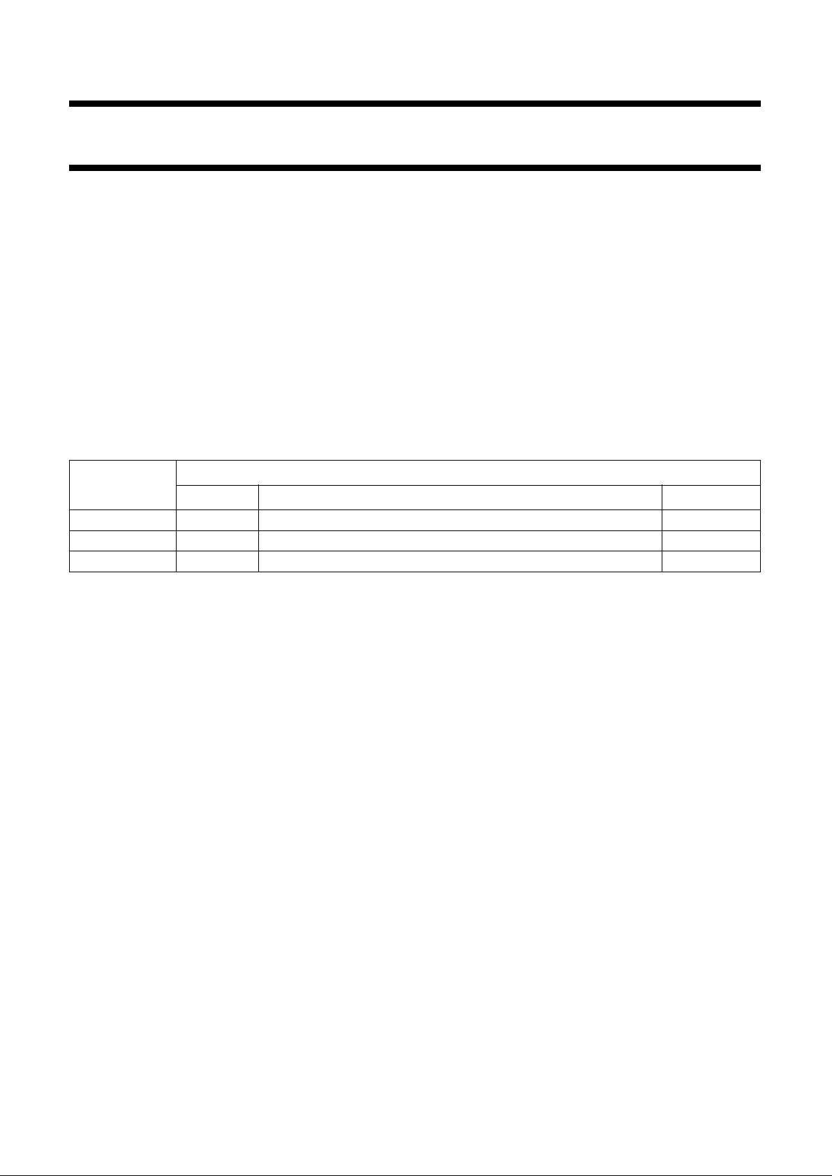
Outputs
The circuit outputs 1 : 2 multiplexed data (duplex) to the
LCD. Generation of BP1 and BP2 (three-level backplane
signals) and the output signals are shown in Fig.4.
The average voltages across the segments are:
1. V
ON(RMS)
= 0.79 V
DD
2. V
OFF(RMS)
= 0.35 VDD.
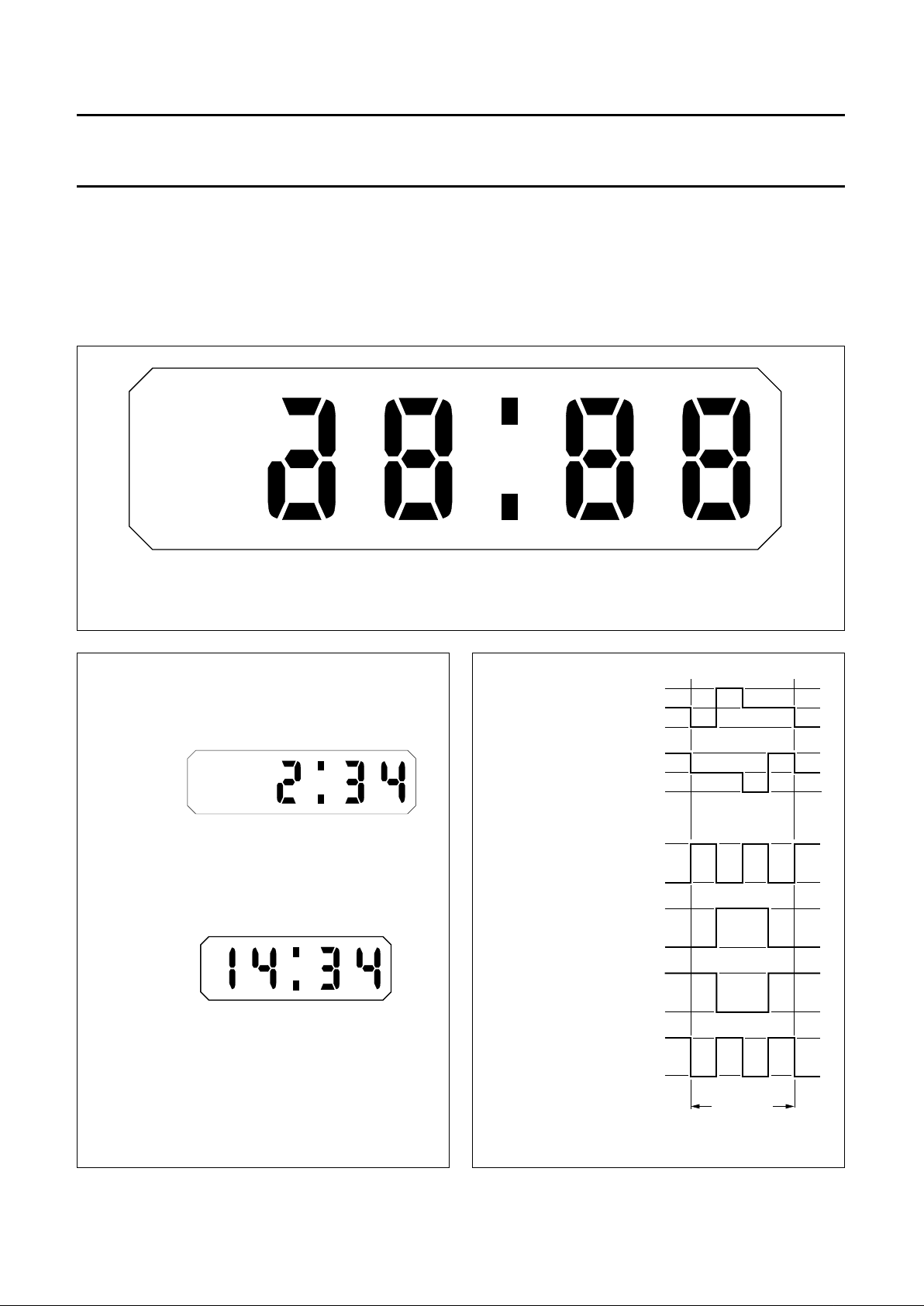
Fig.2 Segment designation of LCD.
MSA992
A2
G2
D2
F2
E2
B2
C2
P1 (P3)
P2 (P4)
A3
G3
D3
F3
E3
B3
C3
A4
G4
D4
F4
E4
B4
C4
AM
PM
A1
G1
D1
E1
B1
C1
Fig.3 Typical displays.
a. 12-hour mode.
b. 24-hour mode.
PM
TIME
MSA993
(a)
MSA994
TIME
(b)
Fig.4 Backplane and output signals.
MSB226
V
DD
VDD/2
0
BP1
V
DD
VDD/2
0
BP2
V
DD
0
SEGMENT1SEGMENT
2
ON ON
V
DD
0
OFF ON
V
DD
0
ON OFF
V
DD
0
OFF OFF
15.625 ms
1997 Apr 16 5
Philips Semiconductors Product specification
4-digit duplex LCD car clock PCF1175C
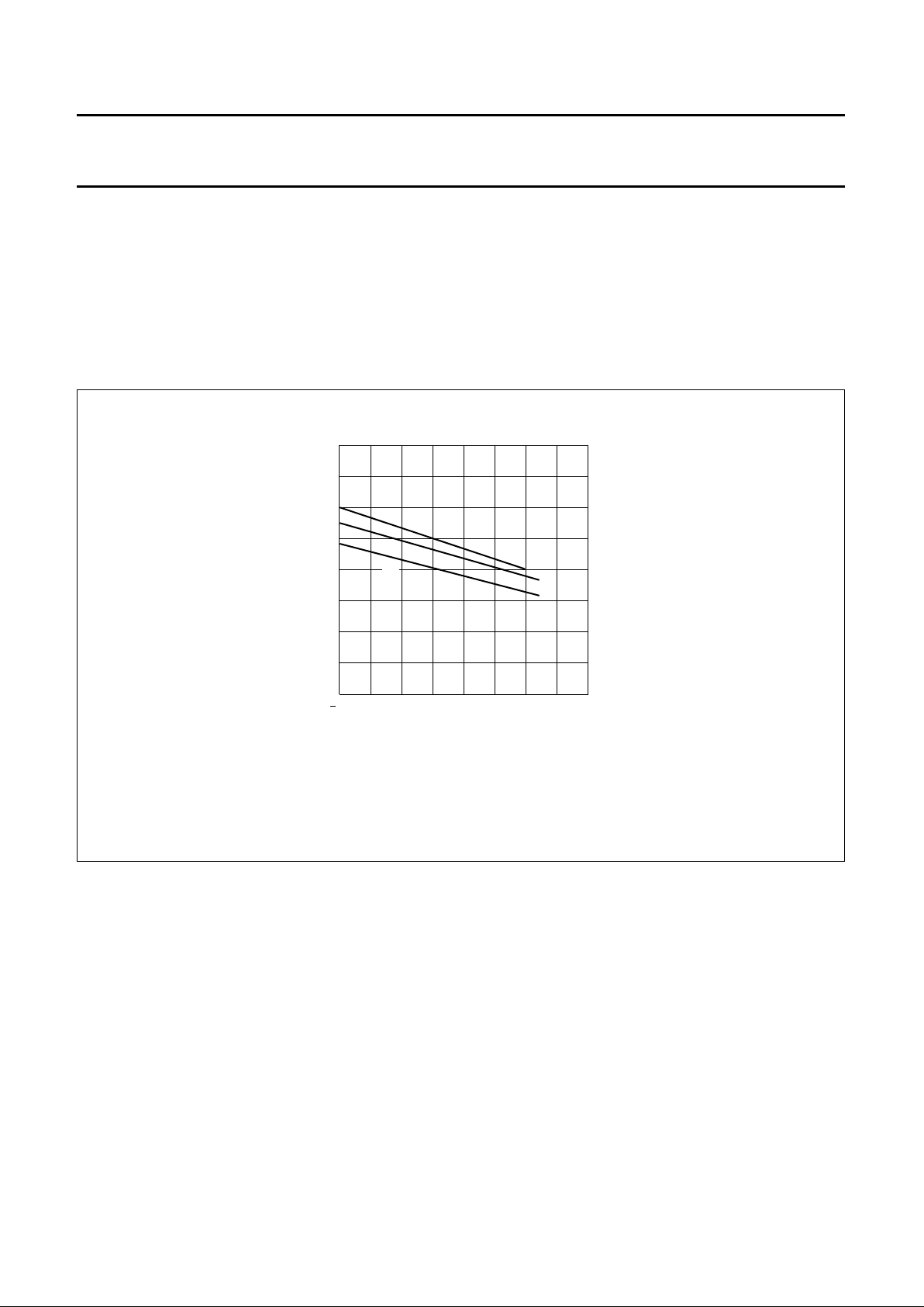
LCD voltage (see Fig.5)
The adjustable voltage regulator controls the supply
voltage (see Section “LCD voltage programming”) in
relation to temperature for good contrast, for example
when VDD= 4.5 V at +25 °C, then:
VDD= 3 to 4 V at +85 °C.
VDD= 5 to 6 V at −40 °C.
Fig.5 Regulated voltage as a function of temperature (typical).
(1) Programmed to 4.0 V at 25 °C (value within the specified operating range).
(2) Programmed to 4.5 V at 25 °C (value within the specified operating range).
(3) Programmed to 5.0 V at 25 °C (value within the specified operating range).
40 0 40 120
−8
−6
−2
0
−4
MSA995
80
T ( C)
o
V
SS
(V)
(2)
(1)
(3)

1997 Apr 16 6
Philips Semiconductors Product specification
4-digit duplex LCD car clock PCF1175C
12/24-hour mode
Operation in 12-hour or 24-hour mode is selected by
connecting MODE to VDD or VSS respectively. If MODE is
left open-circuit and a reset occurs, the mode will change
from 12-hour to 24-hour mode or vice versa.
Power-on
After connecting the supply, the start-up mode is:
MODE connected to V
DD
: 12-hour mode, 1:00 AM.
MODE connected to VSS: 12-hour mode, 0:00.
MODE left open-circuit: 24-hour mode, 0:00 or 1:00.
Colon
If FLASH is connected to V
DD
the colon pulses at 1 Hz.
If FLASH is connected to VSS the colon is static.
Time setting
Switch inputs S1 and S2 have a pull-up resistor to facilitate
the use of single-pole, single-throw contacts. A debounce
circuit is incorporated to protect against contact bounce
and parasitic voltages.
Set enable
Inputs S1 and S2 are enabled by connecting ENABLE to
V
DD
or disabled by connecting to VSS.
Set hours
When S1 is connected to V
SS
the hours displayed
advances by one and after one second continues with one
advance per second until S1 is released (auto-increment).
Set minutes
When S2 is connected to V
SS
the time displayed in
minutes advances by one and after one second continues
with one advance per second until S2 is released
(auto-increment). In addition to minute correction, the
seconds counter is reset to zero.
Segment test/reset
When S1 and S2 are connected to V
SS
, all LCD segments
are switched ON. Releasing switches S1 and S2 resets the
display. No reset occurs when DATA is connected to V
SS
(overlapping S1 and S2).
Test mode
When TS is connected to V
DD
, the device is in normal
operating mode. When connecting TS to VSS all counters
(seconds, minutes and hours) are stopped, allowing quick
testing of the display via S1 and S2 (debounce and
auto-increment times are 64 times faster). TS has a
pull-up resistor but for reasons of safety it should be
connected to VDD.
EEPROM
V
PP
has a pull-up resistor but for reasons of safety it should
be connected to VDD.
LCD voltage programming
To enable LCD voltage programming, SEL is set to
open-circuit and a level of V
DD
− 5 V is applied to VPP (see
Fig.6). The first pulse (tE) applied to the DATA input clears
the EEPROM to give the lowest voltage output. Further
pulses (tL) will increment the output voltage by steps of
typically 150 mV (T
amb
=25°C). For programming,
measure VDD− VSS and apply a store pulse (tW) when the
required value is reached. If the maximum number of steps
(n = 31) is reached and an additional pulse is applied the
voltage will return to the lowest value.
Time calibration
To compensate for the tolerance in the quartz crystal
frequency which has been positively offset (nominal
deviation +60 × 10
−6
) by capacitors at the oscillator input
and output, a number (n) of 262144 Hz are inhibited every
second of operation.
 Loading...