


Philips P87C576EHBB, P87C576EFPN, P87C576EFLKA, P87C576EFFFA, P87C576EFBB Datasheet
...INTEGRATED CIRCUITS
83C576/87C576
80C51 8-bit microcontroller family
8K/256 OTP/ROM, 6 channel 10-bit A/D,
4 comparators, failure detect circuitry, watchdog timer
Product specification |
1998 Jun 04 |
Supersedes data of 1998 Jan 06
IC20 Data Handbook
m n r

Philips Semiconductors Product specification
80C51 8-bit microcontroller family
8K/256 OTP/ROM, 6 channel 10-bit A/D, 4 comparators, |
83C576/87C576 |
failure detect circuitry, watchdog timer |
|
|
|
FEATURES
•80C51 based architecture
±8k × 8 ROM (83C576)
±8k × 8 EPROM (87C576)
±256 × 8 RAM
±10-bit, 6 channel A/D
±Three 16-bit counter/timers
±2 PWM outputs
±Programmable Counter Array
±Universal Peripheral Interface
±Enhanced UART
±Oscillator fail detect
±Low active reset
±4 analog comparators
±Watchdog timer
±Low VCC detect
±Power-on detect
•Memory addressing capability
± 64k ROM and 64k RAM
•Power control modes:
±Idle mode
±Power-down mode
•CMOS and TTL compatible
•6 to 16MHz
•Extended temperature ranges
•OTP available
•That can be programmed in circuit
•Software Reset
•15 source, 2 level interrupt structure
•Lower EMI noise
•Programmable I/O pins
•Serial on-board programming
•Schmitt trigger inputs on Port 1
DESCRIPTION
The Philips 83C576/87C576 is a high-performance microcontroller fabricated with Philips high-density CMOS technology. The Philips CMOS technology combines the high speed and density characteristics of HMOS with the low power attributes of CMOS. Philips epitaxial substrate minimizes latch-up sensitivity.
The 8XC576 contains an 8k × 8 ROM (83C576) EPROM (87C576), a 256 × 8 RAM, 32 I/O lines, three 16-bit counter/timers, a Programmable Counter Array (PCA), a 10-bit, 6 channel A/D,
2 PWM outputs, an 8-bit UPI interface, a fifteen-source, two-priority level nested interrupt structure, an enhanced UART, four analog comparators, power-fail detect and oscillator fail detect circuits, and on-chip oscillator and clock circuits.
In addition, the 8XC576 has a low active reset, and a software reset. There is also a fully configurable watchdog timer, and internal power on clear circuit. The part includes idle mode and power-down mode states for reduced power consumption.
ORDERING INFORMATION
ROM |
EPROM1 |
|
TEMPERATURE RANGE °C AND PACKAGE |
FREQ |
DRAWING |
|
(MHz) |
NUMBER |
|||
|
|
|
|
||
|
|
|
|
|
|
P83C576EBPN |
P87C576EBPN |
OTP |
0 to +70, 40-Pin Plastic Dual In-line Package |
16 |
SOT129-1 |
|
|
|
|
|
|
P83C576EBAA |
P87C576EBAA |
OTP |
0 to +70, 44-Pin Plastic Leaded Chip Carrier |
16 |
SOT187-2 |
|
|
|
|
|
|
P83C576EBBB |
P87C576EBBB |
OTP |
0 to +70, 44-Pin Plastic Quad Flat Pack |
16 |
SOT307-2 |
|
|
|
|
|
|
P83C576EFP N |
P87C576EBPN |
OTP |
±40 to +85, 40-Pin Plastic Dual In-line Package |
16 |
SOT129-1 |
|
|
|
|
|
|
P83C576EFA A |
P87C576EFA A |
OTP |
±40 to +85, 44-Pin Plastic Leaded Chip Carrier |
16 |
SOT187-2 |
|
|
|
|
|
|
P83C576EFB B |
P87C576EFBB |
OTP |
±40 to +85, 44-Pin Plastic Quad Flat Pack |
16 |
SOT307-2 |
|
|
|
|
|
|
P83C576EHPN |
P87C576EHPN |
OTP |
±40 to +125, 40-Pin Plastic Dual In-line Package |
16 |
SOT129-1 |
|
|
|
|
|
|
P83C576EHAA |
P87C576EHAA |
OTP |
±40 to +125, 44-Pin Plastic Leaded Chip Carrier |
16 |
SOT187-2 |
|
|
|
|
|
|
P83C576EHBB |
P87C576EHBB |
OTP |
±40 to +125, 44-Pin Plastic Quad Flat Pack |
16 |
SOT307-2 |
|
|
|
|
|
|
NOTE:
1. OTP - One Time Programmable EPROM.
1998 Jun 04 |
2 |
853-2067 19495 |

Philips Semiconductors Product specification
80C51 8-bit microcontroller family
8K/256 OTP/ROM, 6 channel 10-bit A/D, 4 comparators, |
83C576/87C576 |
failure detect circuitry, watchdog timer |
|
|
|
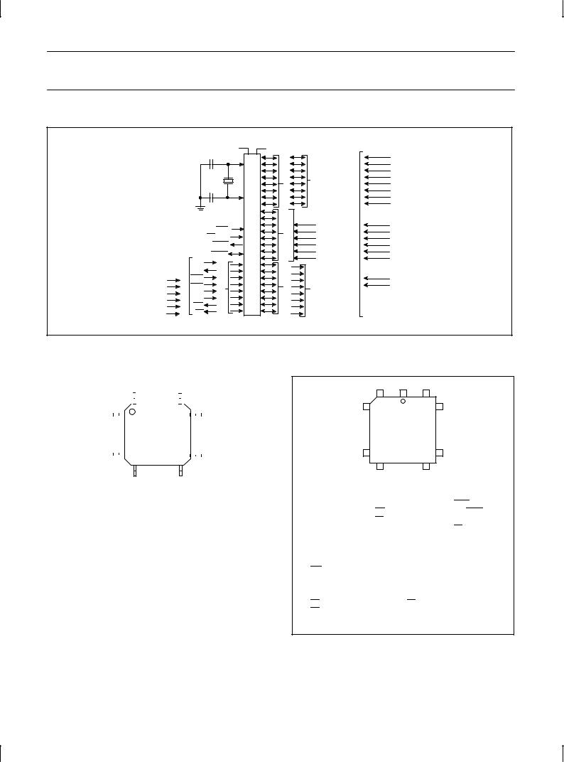
BLOCK DIAGRAM
|
|
|
|
P0.0-P0.7 |
P2.0-P2.7 |
|
|
|
|
|
UPI |
PORT 0 |
PORT 2 |
|
|
|
|
|
CONTROL |
DRIVERS |
DRIVERS |
|
|
|
LOW |
|
POWER |
|
|
|
|
VCC |
VOLTAGE |
|
ON |
|
|
|
|
|
DETECT |
|
DETECT |
|
|
|
|
VSS |
A |
|
B |
|
|
|
|
|
|
|
|
|
|
||
|
RAM ADDR |
RAM |
PORT 0 |
PORT 2 |
|
ROM/ |
|
|
REGISTER |
LATCH |
LATCH |
|
EPROM |
||
|
|
|
|||||
|
B |
|
ACC |
|
|
STACK |
PROGRAM |
|
REGISTER |
|
|
|
POINTER |
ADDRESS |
|
|
|
|
|
|
REGISTER |
||
|
|
|
|
|
|
|
|
|
|
|
|
TMP2 |
TMP1 |
|
BUFFER |
|
|
|
|
ALU |
|
|
PC |
|
|
|
|
|
|
INCRE- |
|
|
WATCHDOG |
|
|
|
|
|
MENTER |
|
TIMER |
|
|
|
|
|
|
|
|
|
B |
PSW |
SFRs |
|
|
|
|
|
|
TIMERS |
|
PROGRAM |
|
|
|
|
A |
|
PCA |
|
|
|
|
|
|
|
COUNTER |
||
PSEN |
|
INSTRUCTION |
REGISTER |
|
|
|
|
ALE |
TIMING |
|
|
|
DPTR |
||
EA |
AND |
|
|
|
|
||
CONTROL |
|
|
|
|
|||
RST |
|
|
|
|
|
||
|
PD |
|
CLK AND OSC |
PORT 1 |
|
PORT 3 |
|
|
|
|
FAILURE |
LATCH |
10-BIT |
LATCH |
PWM |
|
|
|
DETECT |
|
|
||
|
OSCILLATOR |
|
ANALOG TO DIGITAL |
|
|
||
|
|
CONVERTER |
|
|
|||
|
|
|
|
|
|
|
|
|
|
|
|
PORT 1 |
|
PORT 3 |
COMPARATOR |
|
|
|
|
DRIVERS |
|
DRIVERS |
BLOCK |
|
XTAL1 |
|
XTAL2 |
|
|
|
|
|
|
|
|
|
+AVCC |
P3.0-P3.7 |
|
|
|
|
|
P1.0-P1.5 |
|
|
|
|
|
|
|
|
±AVSS |
|
SU00255B |
1998 Jun 04 |
|
|
|
|
3 |
|
|
Philips Semiconductors |
Product specification |
80C51 8-bit microcontroller family
8K/256 OTP/ROM, 6 channel 10-bit A/D, 4 comparators, failure detect circuitry, watchdog timer
LOGIC SYMBOL
|
|
|
VCC |
VSS |
|
|
|
|
XTAL1 |
|
|
|
|
|
|
0 |
ADDRESS AND |
|
|
|
|
PORT |
DATA BUS |
|
|
|
XTAL2 |
1PORT |
FUNCTIONSSECONDARY |
|
|
|
|
|
|
|
|
|
RST |
|
|
|
|
|
EA/VPP |
|
|
|
|
|
PSEN |
|
|
|
FUNCTIONSSECONDARY |
ALE/PROG |
2PORT |
|
|
|
RxD |
3PORT |
|
||
|
|
TxD |
|
|
|
CMP3+ |
|
INT0 |
|
|
|
|
INT1 |
|
|
|
|
CMP2+ |
|
|
|
ADDRESS BUS |
|
CMP1+ |
|
T0 |
|
|
|
|
|
|
|
||
|
T1 |
|
|
|
|
CMPR± |
|
|
|
|
|
|
WR |
|
|
|
|
CMP0+ |
|
|
|
|
|
|
RD |
|
|
|
|
CMP0± |
|
|
|
|
|
|
|
|
|
|
|
83C576/87C576
DB0
DB1
DB2
DB3
DB4
DB5
DB6
DB7
ADIN0
ADIN1
ADIN2
ADIN3
ADIN4
ADIN5
 PWM1/ECI
 CEX4/PWM0
T2/CS#
T2EX/A0
 CEX3/CMP3
 CEX2/CMP2
 CEX1/CMP1
 CEX0/CMP0
SU00254A
PIN CONFIGURATIONS |
|
44-pin Plastic Quad Flat Pack |
Plastic Leaded Chip Carrier |
|
|
|
|
|
|
|
|
44 |
34 |
|
|
|
|
|||||||||||
|
1 |
|
|
|
|
|
|
|
|
|
|
|
|
|
|
|
|
33 |
|
|||||
|
|
|
|
|
|
|
|
|
|
|
|
|
|
|
|
|
|
|||||||
|
|
|
|
|
|
|
|
|
|
|
|
|
|
|
|
|
|
|||||||
|
|
|
|
|
|
|
|
|
|
|
|
|
|
|
|
|
|
|||||||
|
|
|
|
|
|
|
|
PQFP |
|
|||||||||||||||
|
|
|
|
|
|
|
|
|
|
|
|
|
|
|
|
|||||||||
|
11 |
|
12 |
22 |
|
23 |
|
|||||||||||||||||
|
|
|
|
|||||||||||||||||||||
|
|
|
|
|||||||||||||||||||||
|
|
|
|
|||||||||||||||||||||
|
|
|
|
|
|
|
|
|
|
|
||||||||||||||
Pin |
|
Function |
Pin |
Function |
Pin |
Function |
||||||||||||||||||
1 |
ADIN3/P1.3 |
16 |
|
VSS |
31 |
P0.6/AD6/DB6 |
||||||||||||||||||
2 |
ADIN4/P1.4 |
17 |
|
NC* |
32 |
P0.5/AD5/DB5 |
||||||||||||||||||
3 |
ADIN5/P1.5 |
18 |
|
P2.0/A8/CEX0/CMP0 |
33 |
P0.4/AD4/DB4 |
||||||||||||||||||
4 |
|
|
|
|
|
|
|
19 |
|
P2.1/A9/CEX1/CMP1 |
34 |
P0.3/AD3/DB3 |
||||||||||||
RST |
||||||||||||||||||||||||
5 |
RxD/P3.0 |
20 |
|
P2.2/A10/CEX2/CMP2 |
35 |
P0.2/AD2/DB2 |
||||||||||||||||||
6 |
NC* |
21 |
|
|
P2.3/A11/CEX3/CMP3 |
36 |
P0.1/AD1/DB1 |
|||||||||||||||||
7 |
TXD/P3.1 |
22 |
|
|
P2.4/A12/T2EX/A0 |
37 |
P0.0/AD0/DB0 |
|||||||||||||||||
8 |
|
|
|
INT0/P3.2/CMP3+ |
23 |
|
P2.5/A13/T2/CS |
|
|
38 |
VCC |
|||||||||||||
|
|
|
|
|||||||||||||||||||||
9 |
|
|
|
INT1/P3.3/CMP2+ |
24 |
|
P2.6/A14/CEX4/PWM0 |
39 |
NC* |
|||||||||||||||
10 |
|
T0/P3.4/CMP1+ |
25 |
|
P2.7/A15/PWM1/ECI |
40 |
+VREF/AVCC |
|||||||||||||||||
11 |
|
T1/P3.5/CMPR± |
26 |
|
PSEN |
|
|
41 |
±VREF/AVSS |
|||||||||||||||
12 |
|
|
|
WR/P3.6/CMP0+ |
27 |
|
|
|
|
|
|
42 |
ADIN0/P1.0 |
|||||||||||
|
|
|
ALE/PROG |
|||||||||||||||||||||
13 |
|
|
RD/P3.7CMP0± |
28 |
|
NC* |
43 |
ADIN1/P1.1 |
||||||||||||||||
|
|
|||||||||||||||||||||||
14 |
|
XTAL2 |
29 |
|
|
|
|
44 |
ADIN2/P1.2 |
|||||||||||||||
|
|
EA/VPP |
||||||||||||||||||||||
15 |
|
XTAL1 |
30 |
|
P0.7/AD7/DB7 |
|
|
|||||||||||||||||
* NO INTERNAL CONNECTION |
|
|
|
|
|
|
|
|
|
|
|
|
SU00253B |
|||||||||||
|
|
|
|
|
|
|
|
|
|
|
|
|
|
|
|
|
|
|
|
|
|
|
|
|
|
|
|
6 |
1 |
40 |
|
|
|
7 |
|
|
|
|
39 |
|
|
|
|
|
LCC |
|
|
|
|
17 |
|
|
|
|
29 |
|
|
|
|
18 |
|
28 |
|
|
Pin |
Function |
Pin |
Function |
|
Pin |
Function |
|
1 |
NC* |
16 |
T0/P3.4/CMP1+ |
|
31 |
P2.7/A15/PWM1/ECI |
|
2 |
+VREF/AVCC |
17 |
T1/P3.5/CMPR± |
|
32 |
PSEN |
|
3 |
±VREF/AVSS |
18 |
WR/P3.6/CMP0+ |
|
33 |
ALE/PROG |
|
4 |
ADIN0/P1.0 |
19 |
RD/P3.7/CMP0± |
|
34 |
NC* |
|
5 |
ADIN1/P1.1 |
20 |
XTAL2 |
|
|
35 |
EA/VPP |
6 |
ADIN2/P1.2 |
21 |
XTAL1 |
|
|
36 |
P0.7/AD7/DB7 |
7 |
ADIN3/P1.3 |
22 |
VSS |
|
|
37 |
P0.6/AD6/DB6 |
8 |
ADIN4/P1.4 |
23 |
NC* |
|
|
38 |
P0.5/AD5/DB5 |
9 |
ADIN5/P1.5 |
24 |
P2.0/A8/CEX0/CMP0 |
39 |
P0.4/AD4/DB4 |
||
10 |
RST |
25 |
P2.1/A9/CEX1/CMP1 |
40 |
P0.3/AD3/DB3 |
||
11 |
RxD/P3.0 |
26 |
P2.2/A10/CEX2/CMP2 |
41 |
P0.2/AD2/DB2 |
||
12 |
NC* |
27 |
P2.3/A11/CEX3/CMP3 |
42 |
P0.1/AD1/DB1 |
||
13 |
TxD/P3.1 |
28 |
P2.4/A12/T2EX/A0 |
|
43 |
P0.0/AD0/DB0 |
|
14 |
INT0/P3.2/CMP3+ |
29 |
P2.5/A13/T2/CS |
|
44 |
VCC |
|
15 |
INT1/P3.3/CMP2+ |
30 |
P2.6/A14/CEX4/PWM0 |
|
|
||
* NO INTERNAL CONNECTION |
SU00252A |
|
1998 Jun 04 |
4 |

Philips Semiconductors Product specification
80C51 8-bit microcontroller family
8K/256 OTP/ROM, 6 channel 10-bit A/D, 4 comparators, |
|
83C576/87C576 |
||||||||
failure detect circuitry, watchdog timer |
|
|
|
|
|
|||||
|
|
|
|
|
|
|
|
|
|
|
PIN DESCRIPTIONS |
|
|
|
|
|
|
|
|
||
|
|
|
|
|
|
|
|
|
|
|
|
PIN NUMBER |
|
|
|
|
|
|
|
||
|
|
|
|
|
|
|
|
|
||
MNEMONIC |
DIP |
LCC |
QFP |
TYPE |
|
NAME AND FUNCTION |
|
|||
|
|
|
|
|
|
|
|
|
|
|
VSS |
20 |
22 |
16 |
I |
|
Ground: 0V reference. |
|
|
||
VCC |
40 |
44 |
38 |
I |
|
Power Supply: This is the power supply voltage for normal, idle, and power-down operation. |
||||
P0.0-0.7 |
39-32 |
43-36 |
37-30 |
I/O |
|
Port 0: Port 0 is a bidirectional I/O port. Port 0 is also the multiplexed low-order address and |
||||
|
|
|
|
|
|
data bus during accesses to external program and data memory (see Note 5). In this |
||||
|
|
|
|
|
|
application, it uses strong internal pull-ups when emitting 1s. Port 0 also receives code bytes |
||||
|
|
|
|
|
|
during parallel EPROM programming and outputs code bytes during verification. External |
||||
|
|
|
|
|
|
pull-ups are required during program verification. During reset, the port register is loaded |
||||
|
|
|
|
|
|
with 1's. Port 0 has 4 output modes selected on a per bit basis by writing to the P0M1 and |
||||
|
|
|
|
|
|
P0M2 Special Function Registers as follows: |
||||
|
|
|
|
|
|
P0M1.x |
|
P0M2.x |
Mode Description |
|
|
|
|
|
|
|
0 |
0 |
|
Open drain (default). See Note 1. |
|
|
|
|
|
|
|
0 |
1 |
|
Weak pullup. See Note 2. |
|
|
|
|
|
|
|
1 |
0 |
|
High impedance. See Note 3. |
|
|
|
|
|
|
|
1 |
1 |
|
Push-pull. See Note 4. |
|
|
|
|
|
|
|
Port 0 is also the data I/O port for the Universal Peripheral Interface (UPI). When the UPI is |
||||
|
|
|
|
|
|
enabled, port 0 must be configured as High-Z by the user. Input/Output through P0 is |
||||
|
|
|
|
|
|
controlled by pin CS, WR, RD, and A0. Output is push-pull when enabled. |
||||
P1.0-P1.5 |
3-8 |
5-9 |
42-44 |
I/O |
|
Port 1: Port 1 is a 6-bit bidirectional I/O port with Schmitt trigger inputs. Port 1 receives the control |
||||
|
|
|
1-3 |
|
|
signals during program memory verification and parallel EPROM programming. During reset, port |
||||
|
|
|
|
|
|
1 is configured as a high impedance analog input port. Digital push-pull outputs are enabled by |
||||
|
|
|
|
|
|
writing 1's to the P1M1 register. The programmer must take care to prevent digital outputs from |
||||
|
|
|
|
|
|
switching while an A/D conversion is in progress. Port 1 has 3 output modes selected on a per bit |
||||
|
|
|
|
|
|
basis by writing to the P1M1 and P1M2 special function registers as follows: |
||||
|
|
|
|
|
|
P1M1.X |
|
P1M2.X |
Mode Description |
|
|
|
|
|
|
|
0 |
0 |
|
A/D only. (High impedance) |
|
|
|
|
|
|
|
0 |
1 |
|
Digital input only. High impedance (default). |
|
|
|
|
|
|
|
1 |
|
X |
|
Push-pull. |
|
|
|
|
|
|
Port 1 pins also serve alternate functions as follows: |
||||
|
3 |
4 |
42 |
I/O |
|
P1.0/ADIN0 |
|
|
||
|
4 |
5 |
43 |
I/O |
|
P1.1/ADIN1 |
|
|
||
|
5 |
6 |
44 |
I/O |
|
P1.2/ADIN2 |
|
|
||
|
6 |
7 |
1 |
I/O |
|
P1.3/ADIN3 |
|
|
||
|
7 |
8 |
2 |
I/O |
|
P1.4/ADIN4 |
|
|
||
|
8 |
9 |
3 |
I/O |
|
P1.5/ADIN5 |
|
|
||
P2.0-P2.7 |
21-28 |
24-31 |
18-25 |
I/O |
|
Port 2: Port 2 is an 8-bit bidirectional I/O port. Port 2 emits the high-order address byte |
||||
|
|
|
|
|
|
during accesses to external program and data memory that use 16-bit addresses (MOVX |
||||
|
|
|
|
|
|
@DPTR) (see Note 5). In this application, it uses strong internal pull-ups when emitting 1s. |
||||
|
|
|
|
|
|
Port 2 receives the high-order address byte during program verification and parallel EPROM |
||||
|
|
|
|
|
|
programming. During reset, the port 2 pullups are turned on synchronously, and the port |
||||
|
|
|
|
|
|
register is loaded with 1's. Port 2 has the following output modes which can be selected on a |
||||
|
|
|
|
|
|
per bit basis by writing to P2M1 and P2M0: |
||||
|
|
|
|
|
|
P2M1.X |
|
P2M2.X |
Mode Description |
|
|
|
|
|
|
|
0 |
0 |
|
Open drain. See Note 1. |
|
|
|
|
|
|
|
0 |
1 |
|
Weak pullup (default). See Note 2. |
|
|
|
|
|
|
|
1 |
0 |
|
High impedance. See Note 3. |
|
|
|
|
|
|
|
1 |
1 |
|
Push-pull. See Note 4. |
|
|
|
|
|
|
|
Port 2 pins serve alternate functions as follows: |
||||
|
21 |
24 |
18 |
|
|
P2.0 |
CEX0 |
PCA module 0 external I/O |
||
|
|
|
|
|
|
|
CMP0 |
comparator 0 output |
||
|
22 |
25 |
19 |
|
|
P2.1 |
CEX1 |
PCA module 1 external I/O |
||
|
|
|
|
|
|
|
CMP1 |
comparator 1 output |
||
|
23 |
26 |
20 |
|
|
P2.2 |
CEX2 |
PCA module 2 external I/O |
||
|
|
|
|
|
|
|
CMP2 |
comparator 2 output |
||
|
24 |
27 |
21 |
|
|
P2.3 |
CEX3 |
PCA module 3 external I/O |
||
|
|
|
|
|
|
|
CMP3 |
comparator 3 output |
||
|
25 |
28 |
22 |
|
|
P2.4 |
T2EX |
timer 2 capture input |
||
|
|
|
|
|
|
|
A0 |
UPI address input |
||
|
26 |
29 |
23 |
|
|
P2.5 |
T2 |
timer 2 external I/O Ð clock-out (programmable) |
||
|
|
|
|
|
|
|
CS |
|
UPI chip select input |
|
|
27 |
30 |
24 |
|
|
P2.6 |
CEX4 |
PCA module 4 external I/O |
||
|
|
|
|
|
|
|
PWM0 |
Pulse width modulator 0 output |
||
|
28 |
31 |
25 |
|
|
P2.7 |
ECI |
PCA count input |
||
|
|
|
|
|
|
|
PWM1 Pulse width modulator 1 output |
|||
1998 Jun 04 |
5 |

Philips Semiconductors Product specification
80C51 8-bit microcontroller family
|
8K/256 OTP/ROM, 6 channel 10-bit A/D, 4 comparators, |
|
|
|
|
83C576/87C576 |
||||||||||||||||||||||||
|
failure detect circuitry, watchdog timer |
|
|
|
|
|
|
|
|
|
|
|
|
|
|
|
|
|
|
|
||||||||||
|
|
|
|
|
|
|
|
|
|
|
|
|
|
|
|
|
|
|
|
|
|
|
|
|
|
|
|
|
|
|
PIN DESCRIPTIONS (Continued) |
|
|
|
|
|
|
|
|
|
|
|
|
|
|
|
|
|
|
|
|||||||||||
|
|
|
|
|
|
|
|
|
|
|
|
|
|
|
|
|
|
|
|
|
|
|
|
|
|
|
|
|
|
|
|
|
|
|
|
|
|
PIN NUMBER |
|
|
|
|
|
|
|
|
|
|
|
|
|
|
|
|
|
|
|
|
|
||
|
|
|
|
|
|
|
|
|
|
|
|
|
|
|
|
|
|
|
|
|
|
|
|
|
|
|
|
|
||
|
MNEMONIC |
DIP |
LCC |
QFP |
TYPE |
|
NAME AND FUNCTION |
|
|
|
|
|
||||||||||||||||||
|
+VREF/AVCC |
1 |
2 |
40 |
I |
|
|
A/D positive power supply |
||||||||||||||||||||||
|
±VREF/AVSS |
2 |
3 |
41 |
I |
|
|
A/D 0V reference |
|
|
|
|
|
|
||||||||||||||||
|
P3.0-P3.7 |
10-17 |
11, |
5, |
I/O |
|
Port 3: Port 3 is an 8-bit bidirectional I/O port. Port 3 pins that have 1s written to them can |
|||||||||||||||||||||||
|
|
|
|
|
|
|
|
13-19 |
7-13 |
|
|
be used as inputs but will source current when externally pulled low (see DC Electrical |
||||||||||||||||||
|
|
|
|
|
|
|
|
|
|
|
|
Characteristics: IIL). During reset all pins will be synchronously driven high and will remain |
||||||||||||||||||
|
|
|
|
|
|
|
|
|
|
|
|
high until written to by software. Port 3 has the following output modes which can be |
||||||||||||||||||
|
|
|
|
|
|
|
|
|
|
|
|
selected on a per bit basis by writing to P3M1 and P3M2: |
||||||||||||||||||
|
|
|
|
|
|
|
|
|
|
|
|
|
P3M1.X |
|
|
P3M2.X |
Mode Description |
|||||||||||||
|
|
|
|
|
|
|
|
|
|
|
|
0 |
|
|
|
|
0 |
|
|
Open drain. See Note 1. |
||||||||||
|
|
|
|
|
|
|
|
|
|
|
|
0 |
|
|
|
|
1 |
|
|
Weak pullup (default). See Note 2. |
||||||||||
|
|
|
|
|
|
|
|
|
|
|
|
1 |
|
|
|
|
0 |
|
|
High impedance. See Note 3. |
||||||||||
|
|
|
|
|
|
|
|
|
|
|
|
1 |
|
|
|
|
1 |
|
|
Push-pull. See Note 4. |
||||||||||
|
|
|
|
|
|
|
|
|
|
|
|
Port 3 pins serve alternate functions as follows: |
||||||||||||||||||
|
|
|
|
|
|
|
10 |
11 |
5 |
I |
|
|
P3.0 |
RxD |
Serial receive port |
|||||||||||||||
|
|
|
|
|
|
|
11 |
13 |
7 |
O |
|
|
P3.1 |
TxD |
Serial transmit port (enabled only when transmitting serial data) |
|||||||||||||||
|
|
|
|
|
|
|
12 |
14 |
8 |
I |
|
|
P3.2 |
|
|
|
|
|
|
|
External interrupt 0 |
|||||||||
|
|
|
|
|
|
|
|
INT0 |
||||||||||||||||||||||
|
|
|
|
|
|
|
|
|
|
|
|
|
|
|
|
|
|
CMP3+ |
Comparator 3 positive input |
|||||||||||
|
|
|
|
|
|
|
13 |
15 |
9 |
I |
|
|
P3.3 |
|
|
|
|
|
|
External interrupt 1 |
||||||||||
|
|
|
|
|
|
|
|
INT1 |
||||||||||||||||||||||
|
|
|
|
|
|
|
|
|
|
|
|
|
|
|
|
|
|
CMP2+ |
Comparator 2 positive input |
|||||||||||
|
|
|
|
|
|
|
14 |
16 |
10 |
I |
|
|
P3.4 |
T0 |
Timer/counter 0 input |
|||||||||||||||
|
|
|
|
|
|
|
|
|
|
|
|
|
|
|
|
|
|
CMP1+ |
Comparator 1 positive input |
|||||||||||
|
|
|
|
|
|
|
15 |
17 |
11 |
I |
|
|
P3.5 |
T1 |
Timer/counter 1 input |
|||||||||||||||
|
|
|
|
|
|
|
|
|
|
|
|
|
|
|
|
|
|
CMPR± |
Common reference to comparators 1, 2, 3 |
|||||||||||
|
|
|
|
|
|
|
16 |
18 |
12 |
O |
|
|
P3.6 |
|
|
|
|
|
External data memory write strobe |
|||||||||||
|
|
|
|
|
|
|
|
WR |
||||||||||||||||||||||
|
|
|
|
|
|
|
|
|
|
|
|
|
|
|
|
|
|
CMP0+ |
Comparator 0 positive input |
|||||||||||
|
|
|
|
|
|
|
17 |
19 |
13 |
O |
|
|
P3.7 |
|
|
|
|
External data memory read strobe |
||||||||||||
|
|
|
|
|
|
|
|
RD |
||||||||||||||||||||||
|
|
|
|
|
|
|
|
|
|
|
|
|
|
|
|
|
|
CMP0± Comparator 0 negative input |
||||||||||||
|
|
|
|
|
|
|
9 |
10 |
4 |
I |
|
Reset: A low on this pin synchronously resets all port pins to a high state. The pin must be |
||||||||||||||||||
|
RST |
|
||||||||||||||||||||||||||||
|
|
|
|
|
|
|
|
|
|
|
|
held low with the oscillator running for 24 oscillator cycles to initialize the internal registers. |
||||||||||||||||||
|
|
|
|
|
|
|
|
|
|
|
|
An internal diffused resistor to VCC permits a power on reset using only an external |
||||||||||||||||||
|
|
|
|
|
|
|
|
|
|
|
|
capacitor to VSS. RST has a Schmitt trigger input stage to provide additional noise immunity |
||||||||||||||||||
|
|
|
|
|
|
|
|
|
|
|
|
with a slow rising input voltage. |
||||||||||||||||||
|
|
|
|
|
|
30 |
33 |
27 |
I/O |
|
Address Latch Enable/Program Pulse: Output pulse for latching the low byte of the address |
|||||||||||||||||||
|
ALE/PROG |
|
|
|||||||||||||||||||||||||||
|
|
|
|
|
|
|
|
|
|
|
|
during an access to external memory. In normal operation, ALE is emitted at a constant rate |
||||||||||||||||||
|
|
|
|
|
|
|
|
|
|
|
|
of 1/6 the oscillator frequency, and can be used for external timing or clocking. Note that |
||||||||||||||||||
|
|
|
|
|
|
|
|
|
|
|
|
one ALE pulse is skipped during each access to external data memory. ALE is switched off |
||||||||||||||||||
|
|
|
|
|
|
|
|
|
|
|
|
if the bit 0 in the AUXR register (8EH) is set. This pin is also the program pulse input |
||||||||||||||||||
|
|
|
|
|
|
|
|
|
|
|
|
|
(PROG) |
during parallel EPROM programming. (See also Internal Reset on page 24.) |
||||||||||||||||
|
|
|
|
29 |
32 |
26 |
O |
|
Program Store Enable: The read strobe to external program memory. When the device is |
|||||||||||||||||||||
|
PSEN |
|
||||||||||||||||||||||||||||
|
|
|
|
|
|
|
|
|
|
|
|
executing code from the external program memory, |
PSEN |
is activated twice each machine |
||||||||||||||||
|
|
|
|
|
|
|
|
|
|
|
|
cycle, except that two |
PSEN |
activations are skipped during each access to external data |
||||||||||||||||
|
|
|
|
|
|
|
|
|
|
|
|
memory. |
PSEN |
is not activated during fetches from internal program memory. |
||||||||||||||||
|
|
|
31 |
35 |
29 |
I |
|
External Access Enable/Programming Supply Voltage: |
|
must be externally held low |
||||||||||||||||||||
|
EA/VPP |
|
EA |
|||||||||||||||||||||||||||
|
|
|
|
|
|
|
|
|
|
|
|
to enable the device to fetch code from external program memory locations 0000H to |
||||||||||||||||||
|
|
|
|
|
|
|
|
|
|
|
|
1FFFH. If |
EA |
is held high, the device executes from internal program memory unless the |
||||||||||||||||
|
|
|
|
|
|
|
|
|
|
|
|
program counter contains an address greater than 1FFFH. This pin also receives the |
||||||||||||||||||
|
|
|
|
|
|
|
|
|
|
|
|
12.75V programming supply voltage (VPP) during EPROM programming. If this pin is at VPP |
||||||||||||||||||
|
|
|
|
|
|
|
|
|
|
|
|
voltage during reset the device enters the in-circuit programming mode. |
||||||||||||||||||
|
XTAL1 |
19 |
21 |
15 |
I |
|
Crystal 1: Input to the inverting oscillator amplifier and input to the internal clock generator |
|||||||||||||||||||||||
|
|
|
|
|
|
|
|
|
|
|
|
circuits. |
|
|
|
|
|
|
|
|
|
|
|
|
|
|||||
|
XTAL2 |
18 |
20 |
14 |
O |
|
Crystal 2: Output from the inverting oscillator amplifier. |
|||||||||||||||||||||||
NOTES:
1.When Open Drain mode is selected, ports 0 and 2 have weak pulldowns to guarantee positive leakage current (see DC electrical characteristic IIH).
2.When Weak Pullup mode is selected, ports bits that have 1's written to them can be used as inputs but will source current when externally pulled low (see DC electrical characteristic IIL).
3.When High Impedance mode is selected, all pullups and pulldowns are turned off. The only current sourced or sunk by the pin is the parasitic leakage current (see DC electrical characteristic IL2 or ILC, as applicable.
4.When Push-Pull mode is selected, strong pullups are on continuously when emitting 1's (see DC electrical characteristic VOH).
5.When Open-Drain, Weak Pull-up, or Push-pull mode is selected.
1998 Jun 04 |
6 |

Philips Semiconductors Product specification
80C51 8-bit microcontroller family
|
8K/256 OTP/ROM, 6 channel 10-bit A/D, 4 comparators, |
|
|
|
83C576/87C576 |
|
|||||||
|
failure detect circuitry, watchdog timer |
|
|
|
|
|
|
|
|
|
|
||
|
|
|
|
|
|
|
|
|
|
|
|
|
|
|
Table 1. |
87C576 Special Function Registers |
|
|
|
|
|
|
|
|
|||
|
|
|
|
|
|
|
|
|
|
|
|
|
|
|
SYMBOL |
DESCRIPTION |
DIRECT |
BIT ADDRESS, SYMBOL, OR ALTERNATIVE PORT FUNCTION |
RESET |
|
|||||||
|
ADDRESS |
MSB |
|
|
|
|
|
|
LSB |
VALUE |
|
||
|
|
|
|
|
|
|
|
|
|
||||
|
|
|
|
|
|
|
|
|
|
|
|
|
|
|
ACC* |
Accumulator |
E0H |
E7 |
E6 |
E5 |
E4 |
E3 |
E2 |
E1 |
E0 |
00H |
|
|
ADC0H# |
A/D Channel 0 MSB |
AAH |
|
|
|
|
|
|
|
|
00H |
|
|
ADC1H# |
A/D Channel 1 MSB |
ABH |
|
|
|
|
|
|
|
|
00H |
|
|
ADC2H# |
A/D Channel 2 MSB |
ACH |
|
|
|
|
|
|
|
|
00H |
|
|
ADC3H# |
A/D Channel 3 MSB |
ADH |
|
|
|
|
|
|
|
|
00H |
|
|
ADC4H# |
A/D Channel 4 MSB |
AEH |
|
|
|
|
|
|
|
|
00H |
|
|
ADC5H# |
A/D Channel 5 MSB |
AFH |
|
|
|
|
|
|
|
|
00H |
|
|
ADC0L# |
A/D Channel 0 2-LSBits |
9AH |
|
|
|
|
|
|
|
|
00H |
|
|
ADC1L# |
A/D Channel 1 2-LSBits |
9BH |
|
|
|
|
|
|
|
|
00H |
|
|
ADC2L# |
A/D Channel 2 2-LSBits |
9CH |
|
|
|
|
|
|
|
|
00H |
|
|
ADC3L# |
A/D Channel 3 2-LSBits |
9DH |
|
|
|
|
|
|
|
|
00H |
|
|
ADC4L# |
A/D Channel 4 2-LSBits |
9EH |
|
|
|
|
|
|
|
|
00H |
|
|
ADC5L# |
A/D Channel 5 2-LSBits |
9FH |
|
|
|
|
|
|
|
|
00H |
|
|
|
|
|
|
|
|
|
|
|
|
|
|
|
|
ADCON# |
A/D Control |
B1H |
ADF |
ADCE |
AD8M |
AMOD1 |
AMOD0 |
ASCA2 |
ASCA1 |
ASCA0 |
00H |
|
|
ADCS# |
A/D Channel Select |
B2H |
|
|
|
|
|
|
|
|
00H |
|
|
|
|
|
|
|
|
|
|
|
||||
|
|
|
|
|
|
|
|
|
|
|
|
|
|
|
AUXR# |
Auxiliary |
8EH |
± |
± |
± |
± |
SRST |
TXI |
LO |
AO |
xxxx0000B |
|
|
|
|
|
|
|
|
|
|
|
|
|
|
|
|
B* |
B register |
F0H |
F7 |
F6 |
F5 |
F4 |
F3 |
F2 |
F1 |
F0 |
00H |
|
|
CCAP0H# |
Module 0 Capture High |
FAH |
|
|
|
|
|
|
|
|
xxxxxxxxB |
|
|
CCAP1H# |
Module 1 Capture High |
FBH |
|
|
|
|
|
|
|
|
xxxxxxxxB |
|
|
CCAP2H# |
Module 2 Capture High |
FCH |
|
|
|
|
|
|
|
|
xxxxxxxxB |
|
|
CCAP3H# |
Module 3 Capture High |
FDH |
|
|
|
|
|
|
|
|
xxxxxxxxB |
|
|
CCAP4H# |
Module 4 Capture High |
FEH |
|
|
|
|
|
|
|
|
xxxxxxxxB |
|
|
CCAP0L# |
Module 0 Capture Low |
EAH |
|
|
|
|
|
|
|
|
xxxxxxxxB |
|
|
CCAP1L# |
Module 1 Capture Low |
EBH |
|
|
|
|
|
|
|
|
xxxxxxxxB |
|
|
CCAP2L# |
Module 2 Capture Low |
ECH |
|
|
|
|
|
|
|
|
xxxxxxxxB |
|
|
CCAP3L# |
Module 3 Capture Low |
EDH |
|
|
|
|
|
|
|
|
xxxxxxxxB |
|
|
CCAP4L# |
Module 4 Capture Low |
EEH |
|
|
|
|
|
|
|
|
xxxxxxxxB |
|
|
|
|
|
|
|
|
|
|
|
|
|
|
|
|
CCAPM0# |
Module 0 Mode |
DAH |
± |
ECOM |
CAPP |
CAPN |
MAT |
TOG |
PWM |
ECCF |
x0000000B |
|
|
|
|
|
|
|
|
|
|
|
|
|
|
|
|
CCAPM1# |
Module 1 Mode |
DBH |
± |
ECOM |
CAPP |
CAPN |
MAT |
TOG |
PWM |
ECCF |
x0000000B |
|
|
|
|
|
|
|
|
|
|
|
|
|
|
|
|
CCAPM2# |
Module 2 Mode |
DCH |
± |
ECOM |
CAPP |
CAPN |
MAT |
TOG |
PWM |
ECCF |
x0000000B |
|
|
|
|
|
|
|
|
|
|
|
|
|
|
|
|
CCAPM3# |
Module 3 Mode |
DDH |
± |
ECOM |
CAPP |
CAPN |
MAT |
TOG |
PWM |
ECCF |
x0000000B |
|
|
|
|
|
|
|
|
|
|
|
|
|
|
|
|
CCAPM4# |
Module 4 Mode |
DEH |
± |
ECOM |
CAPP |
CAPN |
MAT |
TOG |
PWM |
ECCF |
x0000000B |
|
|
|
|
|
|
|
|
|
|
|
|
|
|
|
|
|
|
|
DF |
DE |
DD |
DC |
DB |
DA |
D9 |
D8 |
|
|
|
|
|
|
|
|
|
|
|
|
|
|
|
|
|
CCON*# |
PCA Counter Control |
D8H |
CF |
CR |
± |
CCF4 |
CCF3 |
CCF2 |
CCF1 |
CCF0 |
00x00000B |
|
|
CH# |
PCA Counter High |
F9H |
|
|
|
|
|
|
|
|
00H |
|
|
|
|
|
|
|
|
|
|
|
||||
|
CL# |
PCA Counter Low |
E9H |
|
|
|
|
|
|
|
|
00H |
|
|
|
|
|
|
|
|
|
|
|
|
|
|
|
|
CMOD# |
PCA Counter Mode |
D9H |
CIDL |
WDTE |
± |
± |
± |
CPS1 |
CPS0 |
ECF |
00xxx000B |
|
|
|
|
|
|
|
|
|
|
|
|
|
|
|
|
|
|
|
C7 |
C6 |
C5 |
C4 |
C3 |
C2 |
C1 |
C0 |
|
|
|
|
|
|
|
|
|
|
|
|
|
|
|
|
|
CMP*# |
Comparator |
C0H |
EC3DP |
EC2DP |
EC1DP |
EC0DP |
C3RO |
C2RO |
C1RO |
C0RO |
00H |
|
|
|
|
|
|
|
|
|
|
|
|
|
|
|
|
CMPE# |
Comparator Enable |
92H |
EC3TDC |
EC2TDC |
EC1TDC |
EC0TDC |
EC3O |
EC2O |
EC1O |
EC0O |
00H |
|
|
DPTR: |
Data Pointer (2 bytes) |
|
|
|
|
|
|
|
|
|
|
|
|
|
|
|
|
|
|
|
|
|
|
|
||
|
DPH |
Data Pointer High |
83H |
|
|
|
|
|
|
|
|
00H |
|
|
DPL |
Data Pointer Low |
82H |
|
|
|
|
|
|
|
|
00H |
|
|
|
|
|
AF |
AE |
AD |
AC |
AB |
AA |
A9 |
A8 |
|
|
|
|
|
|
|
|
|
|
|
|
|
|
|
|
|
IE0*# |
Interrupt Enable 0 |
A8H |
EA |
EC |
ET2 |
ES |
ET1 |
EX1 |
ET0 |
EX0 |
00H |
|
|
|
|
|
|
|
|
|
|
|
|
|
|
|
|
IE1*# |
Interrupt Enable 1 |
E8H |
EOB |
EIB |
EAD |
EC4 |
EC3 |
EC2 |
EC1 |
EC0 |
00H |
|
*SFRs are bit addressable.
# SFRs are modified from or added to the 80C51 SFRs.
1998 Jun 04 |
7 |

Philips Semiconductors Product specification
80C51 8-bit microcontroller family
|
8K/256 OTP/ROM, 6 channel 10-bit A/D, 4 comparators, |
|
|
|
|
|
|
|
|
|
83C576/87C576 |
|||||||||||||
|
failure detect circuitry, watchdog timer |
|
|
|
|
|
|
|
|
|
|
|
|
|
|
|
|
|
|
|
|
|
||
|
|
|
|
|
|
|
|
|
|
|
|
|
|
|
|
|
|
|
|
|
|
|
|
|
|
Table 1. |
87C576 Special Function Registers (Continued) |
|
|
|
|
|
|
|
|
|
|
|
|
|
|
||||||||
|
|
|
|
|
|
|
|
|
|
|
|
|
|
|
|
|
|
|
|
|
|
|
|
|
|
SYMBOL |
DESCRIPTION |
DIRECT |
|
BIT ADDRESS, SYMBOL, OR ALTERNATIVE PORT FUNCTION |
|
RESET |
|||||||||||||||||
|
ADDRESS |
MSB |
|
|
|
|
|
|
|
|
|
|
|
|
|
|
LSB |
VALUE |
||||||
|
|
|
|
|
|
|
|
|
|
|
|
|
|
|
|
|
||||||||
|
|
|
|
|
|
|
|
|
|
|
|
|
|
|
|
|
|
|
|
|
|
|
|
|
|
|
|
|
|
BF |
|
BE |
BD |
BC |
|
BB |
|
BA |
B9 |
B8 |
|
|
|||||||
|
|
|
|
|
|
|
|
|
|
|
|
|
|
|
|
|
|
|
|
|
|
|
|
|
|
IP0* |
Interrupt Priority 0 |
B8H |
± |
|
PPC |
PT2 |
PS |
|
PT1 |
|
PX1 |
PT0 |
|
PX0 |
x0000000B |
||||||||
|
|
|
|
|
|
|
|
|
|
|
|
|
|
|
|
|
|
|
|
|
|
|
|
|
|
IP1*# |
Interrupt Priority 1 |
F8H |
POB |
|
PIB |
PAD |
PC4 |
|
PC3 |
|
PC2 |
PC1 |
|
PC0 |
00H |
||||||||
|
|
|
|
|
|
|
|
|
|
|
|
|
|
|
|
|
|
|
|
|
|
|
|
|
|
|
|
|
87 |
|
86 |
|
85 |
84 |
83 |
|
82 |
|
|
81 |
|
80 |
|
|
|||||
|
|
|
|
|
|
|
|
|
|
|
|
|
|
|
|
|
|
|
|
|
|
|
|
|
|
P0* |
Port 0 |
80H |
AD7 |
AD6 |
AD5 |
AD4 |
|
AD3 |
|
AD2 |
AD1 |
|
AD0 |
FFH |
|||||||||
|
|
|
|
|
|
|
|
|
|
|
|
|
|
|
|
|
|
|
|
|
|
|
|
|
|
|
|
|
97 |
|
96 |
|
95 |
94 |
93 |
|
92 |
|
|
91 |
|
90 |
|
|
|||||
|
|
|
|
|
|
|
|
|
|
|
|
|
|
|
|
|
|
|
|
|
|
|
||
|
P1* |
Port 1 |
90H |
± |
|
± |
|
ADIN5 |
ADIN4 |
ADIN3 |
ADIN2 |
ADIN1 |
|
ADIN0 |
FFH |
|||||||||
|
|
|
|
|
|
|
|
|
|
|
|
|
|
|
|
|
|
|
|
|
|
|
|
|
|
|
|
|
|
A7 |
|
A6 |
A5 |
A4 |
|
A3 |
|
A2 |
A1 |
A0 |
|
|
|||||||
|
|
|
|
|
|
|
|
|
|
|
|
|
|
|
|
|
|
|
|
|
|
|
||
|
P2* |
Port 2 |
A0H |
ECI |
CEX4 |
T2 |
T2EX |
CEX3 |
CEX2 |
CEX1 |
|
CEX0 |
FFH |
|||||||||||
|
|
|
|
|
|
|
|
|
|
|
|
|
|
|
|
|
|
|
|
|
|
|
|
|
|
|
|
|
|
B7 |
|
B6 |
B5 |
B4 |
|
B3 |
|
B2 |
B1 |
B0 |
|
|
|||||||
|
|
|
|
|
|
|
|
|
|
|
|
|
|
|
|
|
|
|
|
|
|
|
||
|
P3* |
Port 3 |
B0H |
|
RD |
|
|
WR |
|
T1 |
T0 |
|
INT1 |
|
|
INT0 |
|
|
TxD |
|
RxD |
FFH |
||
|
P0M1# |
Port 0 Output Mode 1 |
84H |
|
|
|
|
|
|
|
|
|
|
|
|
|
|
|
|
|
|
|
00H |
|
|
P0M2# |
Port 0 Output Mode 2 |
85H |
|
|
|
|
|
|
|
|
|
|
|
|
|
|
|
|
|
|
|
00H |
|
|
P1M1# |
Port 1 Output Mode 1 |
94H |
|
|
|
|
|
|
|
|
|
|
|
|
|
|
|
|
|
|
|
00H |
|
|
P1M2# |
Port 1 Output Mode 2 |
95H |
|
|
|
|
|
|
|
|
|
|
|
|
|
|
|
|
|
|
|
3FH |
|
|
P2M1# |
Port 2 Output Mode 1 |
A4H |
|
|
|
|
|
|
|
|
|
|
|
|
|
|
|
|
|
|
|
00H |
|
|
P2M2# |
Port 2 Output Mode 2 |
A5H |
|
|
|
|
|
|
|
|
|
|
|
|
|
|
|
|
|
|
|
FFH |
|
|
P3M1# |
Port 3 Output Mode 1 |
B4H |
|
|
|
|
|
|
|
|
|
|
|
|
|
|
|
|
|
|
|
00H |
|
|
P3M2# |
Port 3 Output Mode 2 |
B5H |
|
|
|
|
|
|
|
|
|
|
|
|
|
|
|
|
|
|
|
FFH |
|
|
|
|
|
|
|
|
|
|
|
|
|
|
|
|
||||||||||
|
PCON |
Power Control |
87H |
SMOD1 |
SMOD0 |
OSF1 |
POF1 |
LVF1 |
WDT0F1 |
PD |
|
IDL |
00xxxx00B |
|||||||||||
|
|
|
|
|
D7 |
|
D6 |
D5 |
D4 |
|
D3 |
|
D2 |
D1 |
D0 |
|
|
|||||||
|
|
|
|
|
|
|
|
|
|
|
|
|
|
|
|
|
|
|
|
|||||
|
PSW* |
Program Status Word |
D0H |
|
CY |
|
AC |
F0 |
RS1 |
|
RS0 |
|
OV |
± |
|
P |
00H |
|||||||
|
|
|
|
|
|
|
|
|
|
|
|
|
|
|
|
|
|
|||||||
|
PWCON# |
PWM Control |
BCH |
± |
|
± |
|
± |
± |
PWMF |
|
|
|
PWE1 |
|
PWE0 |
00H |
|||||||
|
|
|
EN/CLR |
|
||||||||||||||||||||
|
PWMP# |
PWM Prescaler |
BDH |
|
|
|
|
|
|
|
|
|
|
|
|
|
|
|
|
|
|
|
00H |
|
|
|
|
|
|
|
|
|
|
|
|
|
|
|
|
|
|
|
|
|
|||||
|
PWM0# |
PWM Register 0 |
BEH |
|
|
|
|
|
|
|
|
|
|
|
|
|
|
|
|
|
|
|
00H |
|
|
PWM1# |
PWM Register 1 |
BFH |
|
|
|
|
|
|
|
|
|
|
|
|
|
|
|
|
|
|
|
00H |
|
|
RACAP2H# |
Timer 2 Capture High |
CBH |
|
|
|
|
|
|
|
|
|
|
|
|
|
|
|
|
|
|
|
00H |
|
|
RACAP2L# |
Timer 2 Capture Low |
CAH |
|
|
|
|
|
|
|
|
|
|
|
|
|
|
|
|
|
|
|
00H |
|
|
SADDR# |
Slave Address |
A9H |
|
|
|
|
|
|
|
|
|
|
|
|
|
|
|
|
|
|
|
00H |
|
|
SADEN# |
Slave Address Mask |
B9H |
|
|
|
|
|
|
|
|
|
|
|
|
|
|
|
|
|
|
|
00H |
|
|
SBUF |
Serial Data Buffer |
99H |
|
|
|
|
|
|
|
|
|
|
|
|
|
|
|
|
|
|
|
xxxxxxxxB |
|
|
|
|
|
|
9F |
|
9E |
9D |
9C |
|
9B |
|
9A |
99 |
|
98 |
|
|
||||||
|
|
|
|
|
|
|
|
|
|
|
|
|
|
|
||||||||||
|
SCON* |
Serial Control |
98H |
SM0/FE |
SM1 |
SM2 |
REN |
|
TB8 |
|
RB8 |
TI |
|
RI |
00H |
|||||||||
|
SP |
Stack Pointer |
81H |
|
|
|
|
|
|
|
|
|
|
|
|
|
|
|
|
|
|
|
07H |
|
|
|
|
|
|
|
|
|
|
|
|
|
|
|
|
|
|
|
|
|
|||||
|
|
|
|
|
8F |
|
8E |
8D |
8C |
|
8B |
|
8A |
89 |
|
88 |
|
|
||||||
|
|
|
|
|
|
|
|
|
|
|
|
|
|
|
||||||||||
|
TCON* |
Timer Control |
88H |
TF1 |
TR1 |
TF0 |
TR0 |
|
IE1 |
|
IT1 |
IE0 |
|
IT0 |
00H |
|||||||||
|
|
|
|
|
|
|
|
|
|
|
|
|
|
|
|
|
|
|
||||||
|
|
|
|
|
CF |
|
CE |
CD |
CC |
|
CB |
|
CA |
C9 |
C8 |
|
|
|||||||
|
|
|
|
|
|
|
|
|
|
|
|
|
|
|||||||||||
|
T2CON* |
Timer 2 Control |
C8H |
TF2 |
EXF2 |
RCLK |
TCLK |
EXEN2 |
|
TR2 |
C/T2 |
|
CP/RL2 |
00H |
||||||||||
|
|
|
|
|
|
|
|
|
|
|
|
|
|
|
|
|
|
|
||||||
|
T2MOD# |
Timer 2 Mode Control |
C9H |
± |
|
± |
|
± |
± |
± |
|
± |
|
|
T2OE2 |
|
DCEN |
xxxxxxx0B |
||||||
*SFRs are bit addressable.
# SFRs are modified from or added to the 80C51 SFRs.
1.Reset value depends on reset source.
2.Programmable clock-out
1998 Jun 04 |
8 |

Philips Semiconductors Product specification
80C51 8-bit microcontroller family
|
8K/256 OTP/ROM, 6 channel 10-bit A/D, 4 comparators, |
|
|
|
83C576/87C576 |
|
|||||||
|
failure detect circuitry, watchdog timer |
|
|
|
|
|
|
|
|
|
|
||
|
|
|
|
|
|
|
|
|
|
|
|
|
|
|
Table 1. |
87C576 Special Function Registers (Continued) |
|
|
|
|
|
|
|
||||
|
|
|
|
|
|
|
|
|
|
|
|
|
|
|
SYMBOL |
DESCRIPTION |
DIRECT |
BIT ADDRESS, SYMBOL, OR ALTERNATIVE PORT FUNCTION |
RESET |
|
|||||||
|
ADDRESS |
MSB |
|
|
|
|
|
|
LSB |
VALUE |
|
||
|
|
|
|
|
|
|
|
|
|
||||
|
TH0 |
Timer High 0 |
8CH |
|
|
|
|
|
|
|
|
00H |
|
|
TH1 |
Timer High 1 |
8DH |
|
|
|
|
|
|
|
|
00H |
|
|
TH2# |
Timer High 2 |
CDH |
|
|
|
|
|
|
|
|
00H |
|
|
TL0 |
Timer Low 0 |
8AH |
|
|
|
|
|
|
|
|
00H |
|
|
TL1 |
Timer Low 1 |
8BH |
|
|
|
|
|
|
|
|
00H |
|
|
TL2# |
Timer Low 2 |
CCH |
|
|
|
|
|
|
|
|
00H |
|
|
|
|
|
|
|
|
|
|
|
|
|
|
|
|
TMOD |
Timer Mode |
89H |
GATE |
C/T |
M1 |
M0 |
GATE |
C/T |
M1 |
M0 |
00H |
|
|
UCS# |
UPI Control/Status |
86H |
|
|
|
|
|
|
|
|
00H |
|
|
ST7 |
ST6 |
ST5 |
ST4 |
UE |
AF |
IBF |
OBE/OBF |
|
||||
|
|
|
|
|
|
|
|
|
|
|
|
|
|
|
|
|
|
|
|
|
|
|
|
|
|
|
|
|
WDCON# |
Watchdog Timer Control |
C4H |
PRE2 |
PRE1 |
PRE0 |
LVRE |
OFRE |
DPD |
WDRUN |
WDMOD |
11111111B |
|
|
WDL# |
Watchdog Timer Reload |
C1H |
|
|
|
|
|
|
|
|
00H |
|
|
|
|
|
|
|
|
|
|
|
||||
|
WFEED1# |
Watchdog Feed 1 |
C2H |
|
|
|
|
|
|
|
|
xxH |
|
|
WFEED2# |
Watchdog Feed 2 |
C3H |
|
|
|
|
|
|
|
|
xxH |
|
*SFRs are bit addressable.
# SFRs are modified from or added to the 80C51 SFRs. 1. Reset value depends on reset source.
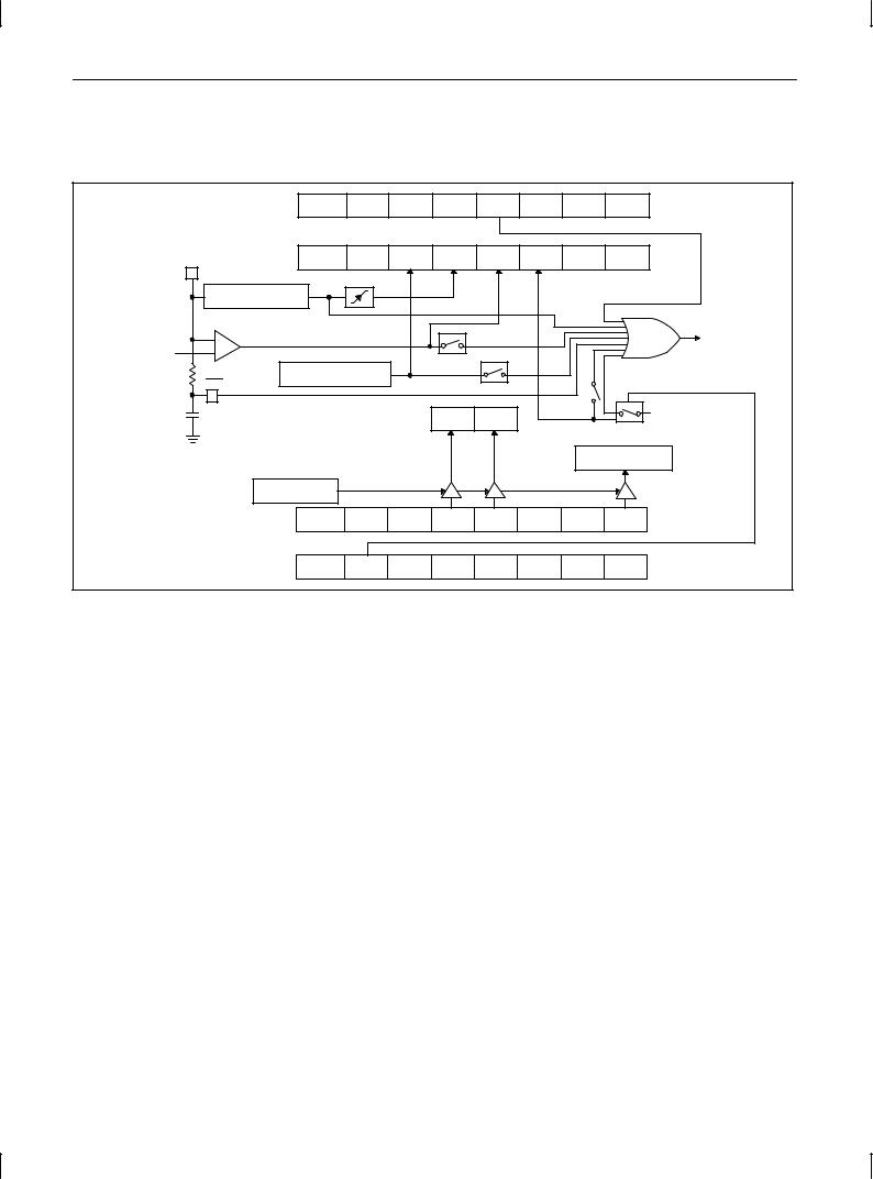
The 8XC576 has a number of failure detect circuits to prevent abnormal operating conditions. these failure detect circuits generate resets as shown in Figure 1.
POWER ON CLEAR / POWER ON FLAG
An on-chip Power On Detect Circuit resets the 8XC576 and sets the Power Off Flag (PCON.4) on power up or if VCC drops to zero momentarily. The POF can only be cleared by software. The RST pin is not driven by the power on detect circuit. The POF can be read by software to determine that a power failure has occurred and can also be set by software.
LOW VOLTAGE DETECT
An on-chip Low Voltage Detect circuit sets the Low Voltage Flag (PCON.3) if VCC drops below VLOW (see DC Electrical Characteristics) and resets the 8XC576 if the Low Voltage Reset Enable bit (WDCON.4) is set. If the LVRE is cleared, the reset is disabled but LVF will still be set if VCC is low. The RST pin is not driven by the low voltage detect circuit. The LVF can be read by software to determine that VCC was low. The LVF can be set or cleared by software.
OSCILLATOR FAIL DETECT
An on-chip Oscillator Fail Detect circuit sets the Oscillator Fail Flag (PCON.5) if the oscillator frequency drops below OSCF for one or more cycles (see AC Electrical Characteristics: OSCF) and resets the 8XC576 if the Oscillator Fail Reset Enable bit (WDCON.3) is set. If OFRE is cleared, the reset is disabled but OSF will still be set if the oscillator fails. The RST pin is not driven by the oscillator fail detect circuit. The OSF can be read by software to determine that an oscillator failure has occurred. The OSF can be set or cleared by software.
LOW ACTIVE RESET
One of the most notable features on this part is the low active reset. The low active reset operates exactly the same as high active reset with the exception that the part is put into the reset mode by applying a low level to the reset pin. For power-on reset it is also necessary to invert the power-on reset circuit; connecting the 8.2K resistor from the reset pin to VCC and the 10μf capacitor from the reset pin to ground. Figure 1 shows the reset related circuitry.
When reset the port pins on the 8XC576 are driven high synchronously.
The 8XC576 also has Low voltage detection circuitry that will, if enabled, force the part to reset when VCC (on the part) fails below a set level. Low Voltage Reset is enabled by a normal reset. Low Voltage Reset can be disabled by clearing LVRE (bit 4 in the WDCON SFR) then executing a watchdog feed sequence (A5H to WFEED1 followed immediately by 5AH to WFEED2). In addition there is a flag (LVF) that is set if a low voltage condition is detected. The LVF flag is set even if the Low Voltage detection circuitry is disabled. Notice that the Low voltage detection circuitry does not drive the RST# pin so the LVF flag is the only way that the microcontroller can determine if it has been reset due to a low voltage condition.
The 8XC576 has an on-chip power-on detection circuit that sets the POF (PCON.4) flag on power up or if the VCC level momentarily drops to 0V. This flag can be used to determine if the part is being started from a power-on (cold start) or if a reset has occurred due to another condition (warm start).
The 8XC576 can be reset in software by setting the RST bit of the AUXR register (AUXR.3). See Figure 1 for reset diagram.
1998 Jun 04 |
9 |
Philips Semiconductors Product specification
80C51 8-bit microcontroller family
8K/256 OTP/ROM, 6 channel 10-bit A/D, 4 comparators, |
83C576/87C576 |
failure detect circuitry, watchdog timer |
|
|
|
|
|
± |
± |
± |
± |
SRST |
TXI |
LO |
AO |
AUXR |
|
|
(8EH) |
||||||||
|
|
|
|
|
|
|
|
|
|
|
|
VCC |
SMOD1 |
SMOD0 |
OSF |
POF |
LVF |
WDTOF |
PD |
IDL |
PCON |
|
|
(87H) |
||||||||
|
|
|
|
|
|
|
|
|
|
|
|
|
POWER-ON DETECT |
|
|
|
|
|
|
|
|
|
|
+ |
|
|
|
|
|
|
|
8xC576 |
VLOW |
|
|
|
|
|
|
|
|
INTERNAL |
|
|
± |
|
|
|
|
|
|
|
RESET |
|
(LOW VCC |
|
|
|
|
|
|
|
|
||
|
|
|
|
|
|
|
|
|
REFERENCE)
|
OSC FREQ BELOW OSCF |
|
|
|
|
|
|
|
|
RST |
(MIN FREQUENCY) |
|
|
|
|
|
|
WDTE |
|
|
|
|
|
|
|
|
|
||
|
|
|
|
|
|
|
|
|
|
|
|
SHADOW REGISTER |
|
|
|
|
|
PCA WATCHDOG |
|
|
|
FOR WDCON |
|
|
|
|
|
WATCHDOG TIMER |
|
|
|
|
|
|
|
|
SHADOW REGISTER |
||
|
WATCHDOG FEED |
|
|
|
|
|
|
|
|
|
PRE2 |
PRE1 |
PRE0 |
LVRE |
OFRE |
DPD |
WDRUN |
WDMOD |
WDCON |
|
(C4H) |
||||||||
|
|
|
|
|
|
|
|
|
|
|
CIDL |
WDTE |
± |
± |
± |
CPS1 |
CPS0 |
ECF |
CMOD |
|
(D9H) |
||||||||
|
|
|
|
|
|
|
|
|
|
SU00515B
Figure 1. Reset Circuitry
TIMERS
The 8XC576 has four on-chip timers.
Timers 0 and 1 are identical in every way to Timers 0 and 1 on the 80C51.
Timer 2 on the 8XC576 is identical to the 80C52 Timer 2 (described in detail in the 80C52 overview) with the exception that it is an up or down counter. To configure the Timer to count down the DCEN bit in the T2MOD special function register must be set and a low level must be present on the T2EX pin (P1.1).
The Pulse Width Modulator (PWM) system can be used as a timer by disabling its outputs and monitoring its counter overflow flag, the PWMF bit in the PWCON register (see the PWM section for details).
The Watchdog timer operation and implementation is similar to the 8XC550 (for additional information see the 8XC550 datasheet) with the exception that the reset values of the WDCON and WDL special function registers have been changed. The changes in these registers cause the watchdog timer to be enabled with a timeout of 16384 × TOSC when the part is reset. The watchdog can be disabled by executing a valid feed sequence and then clearing WDRUN (bit 2 in the WDCON SFR). In timer mode, the timer is controlled by toggling the WDRUN bit. The timeout flag, WDTOF, is set when the timer overflows and must be cleared in software.
PROGRAMMABLE COUNTER ARRAY (PCA)
The Programmable Counter Array is a special Timer that has five 16-bit capture/compare modules associated with it. Each of the modules can be programmed to operate in one of four modes: rising and/or falling edge capture, software timer, high-speed output, or pulse width modulator. Each module has a pin associated with it in port 2. Module 0 is connected to P2.0(CEX0), module 1 to P2.1(CEX1), etc. The basic PCA configuration is shown in Figure 2.
The PCA timer is a common time base for all five modules and can be programmed to run at: 1/12 the oscillator frequency, 1/4 the oscillator frequency, the Timer 0 overflow, or the input on the ECI pin (P2.7). The timer count source is determined from the CPS1 and CPS0 bits in the CMOD SFR as follows (see Figure 3):
CPS1 CPS0 PCA Timer Count Source
0 |
0 |
1/12 oscillator frequency |
01 1/4 oscillator frequency
10 Timer 0 overflow
1 |
1 |
External Input at ECI pin (P2.7) |
In the CMOD SFR are three additional bits associated with the PCA. They are CIDL which allows the PCA to stop during idle mode, WDTE which enables or disables the watchdog function on
module 4, and ECF which when set causes an interrupt and the PCA overflow flag CF (in the CCON SFR) to be set when the PCA timer overflows. These functions are shown in Figure 3.
The watchdog timer function is implemented in module 4 as implemented in other parts that have a PCA that are available on the market. However, if a watchdog timer is required in the target application, it is recommended to use the hardware watchdog timer that is implemented on the 87C576 separately from the PCA (see Figure 15).
The CCON SFR contains the run control bit for the PCA and the flags for the PCA timer (CF) and each module (refer to Figure 6). To run the PCA the CR bit (CCON.6) must be set by software. The PCA is shut off by clearing this bit. The CF bit (CCON.7) is set when the PCA counter overflows and an interrupt will be generated if the ECF bit in the CMOD register is set, The CF bit can only be cleared by software. Bits 0 through 4 of the CCON register are the flags for the modules (bit 0 for module 0, bit 1 for module 1, etc.) and are set by hardware when either a match or a capture occurs. These flags
1998 Jun 04 |
10 |
Philips Semiconductors Product specification
80C51 8-bit microcontroller family
8K/256 OTP/ROM, 6 channel 10-bit A/D, 4 comparators, |
83C576/87C576 |
failure detect circuitry, watchdog timer |
|
|
|
also can only be cleared by software. The PCA interrupt system shown in Figure 4.
Each module in the PCA has a special function register associated with it. These registers are: CCAPM0 for module 0, CCAPM1 for module 1, etc. (see Figure 7). The registers contain the bits that control the mode that each module will operate in. The ECCF bit (CCAPMn.0 where n=0, 1, 2, 3, or 4 depending on the module) enables the CCF flag in the CCON SFR to generate an interrupt when a match or compare occurs in the associated module. PWM (CCAPMn.1) enables the pulse width modulation mode. The TOG bit (CCAPMn.2) when set causes the CEX output associated with the module to toggle when there is a match between the PCA counter and the module's capture/compare register. The match bit MAT (CCAPMn.3) when set will cause the CCFn bit in the CCON register to be set when there is a match between the PCA counter and the module's capture/compare register.
The next two bits CAPN (CCAPMn.4) and CAPP (CCAPMn.5) determine the edge that a capture input will be active on. The CAPN bit enables the negative edge, and the CAPP bit enables the positive edge. If both bits are set both edges will be enabled and a capture will occur for either transition. The last bit in the register ECOM (CCAPMn.6) when set enables the comparator function. Figure 8 shows the CCAPMn settings for the various PCA functions.
There are two additional registers associated with each of the PCA modules. They are CCAPnH and CCAPnL and these are the registers that store the 16-bit count when a capture occurs or a compare should occur. When a module is used in the PWM mode these registers are used to control the duty cycle of the output.
PCA Capture Mode
To use one of the PCA modules in the capture mode either one or both of the CCAPM bits CAPN and CAPP for that module must be set. The external CEX input for the module (on port 2) is sampled for a transition. When a valid transition occurs the PCA hardware loads the value of the PCA counter registers (CH and CL) into the module's capture registers (CCAPnL and CCAPnH). If the CCFn bit for the module in the CCON SFR and the ECCFn bit in the CCAPMn SFR are set then an interrupt will be generated. Refer to Figure 9.
16-bit Software Timer Mode
The PCA modules can be used as software timers by setting both the ECOM and MAT bits in the modules CCAPMn register. The PCA timer will be compared to the module's capture registers and when a match occurs an interrupt will occur if the CCFn (CCON SFR) and the ECCFn (CCAPMn SFR) bits for the module are both set (see Figure 10).
High Speed Output Mode
In this mode the CEX output (on port 2) associated with the PCA module will toggle each time a match occurs between the PCA counter and the module's capture registers. To activate this mode the TOG, MAT, and ECOM bits in the module's CCAPMn SFR must be set (see Figure 11).
Pulse Width Modulator Mode
All of the PCA modules can be used as PWM outputs. Figure 12 shows the PWM function. The frequency of the output depends on the source for the PCA timer. All of the modules will have the same frequency of output because they all share the PCA timer. The duty cycle of each module is independently variable using the module's capture register CCAPLn. When the value of the PCA CL SFR is less than the value in the module's CCAPLn SFR the output will be low, when it is equal to or greater than the output will be high. When CL overflows from FF to 00, CCAPLn is reloaded with the value in CCAPHn. the allows updating the PWM without glitches. The PWM and ECOM bits in the module's CCAPMn register must be set to enable the PWM mode.
PCA Interrupt System
The PCA on most 80C51 family devices provides a single interrupt source, EC (IE.6). The 8xC576 expands the flexibility of the PCA by providing additional interrupt sources for each of the five PCA modules, EC0 (IE1.0) through EC4 (IE1.4), in addition to the original interrupt source EC (IE.6). Any of these sources can be enabled at any time. It is possible for both a module source (EC0 through EC4) to be enabled at the same time that the single source, EC, is enabled. In this case, a module event will generate an interrupt for both the module source and the single source, EC.
|
|
|
|
16 BITS |
|
|
|
|
|
P2.0/CEX0 |
|
|
|
|
|
|
|
|
|
||
|
|
|
|
|
|
|
|
|
|
|
|
|
|
|
MODULE 0 |
|
|
|
|
||
|
|
|
|
|
|
|
|
|||
|
|
|
|
|
||||||
|
|
|
|
|
|
|
|
|
|
P2.1/CEX1 |
|
|
|
|
|
|
|
|
|
|
|
|
16 BITS |
|
MODULE 1 |
|
|
|
|
|||
|
|
|
|
|
|
|||||
|
|
|
|
|
||||||
|
|
|
|
|
|
|
|
P2.2/CEX2 |
||
|
|
|
|
|
|
|
||||
|
|
|
|
|
|
|
|
|
|
|
|
PCA TIMER/COUNTER |
|
|
MODULE 2 |
|
|
|
|
||
|
|
|
|
|
|
|
||||
|
|
|
|
|||||||
|
|
|
|
|
|
|
|
|
|
|
|
|
|
|
|
|
|
|
|
|
|
TIME BASE FOR PCA MODULES |
|
|
|
|
|
|
|
P2.3/CEX3 |
||
|
|
|
|
MODULE 3 |
|
|
|
|
||
|
|
|
|
|
|
|
||||
|
|
|
|
|
|
|
|
|
|
|
MODULE FUNCTIONS: |
|
|
|
|
|
|
|
|
||
16-BIT CAPTURE |
|
|
|
|
|
|
|
|
||
|
|
|
|
|
|
|
|
|||
16-BIT TIMER |
|
MODULE 4 |
|
|
|
|
P2.6/CEX4 |
|||
|
|
|
|
|||||||
16-BIT HIGH SPEED OUTPUT |
|
|
|
|
|
|
|
|
||
8-BIT PWM |
|
|
|
|
|
|
|
|
||
WATCHDOG TIMER (MODULE 4 ONLY) |
|
|
|
|
|
|
|
SU00578 |
||
|
|
|
|
|
|
|
|
|
|
|
|
|
|
|
|
|
|
|
|
|
|
Figure 2. Programmable Counter Array (PCA)
1998 Jun 04 |
11 |
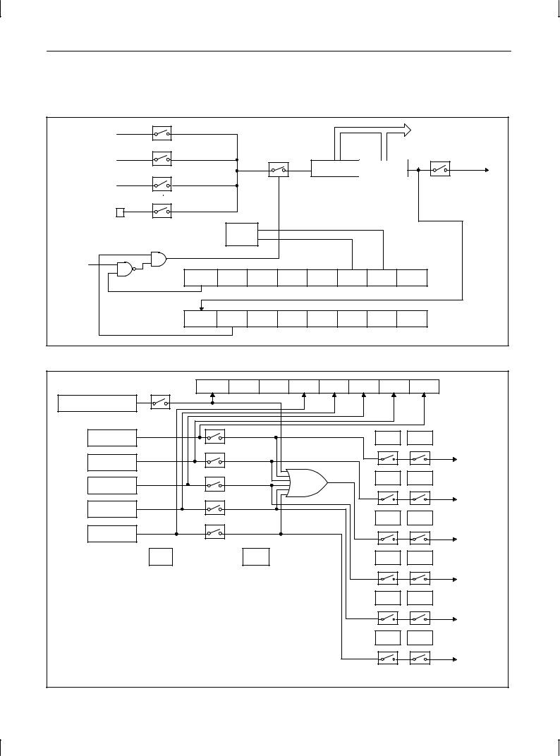
Philips Semiconductors Product specification
80C51 8-bit microcontroller family
8K/256 OTP/ROM, 6 channel 10-bit A/D, 4 comparators, |
83C576/87C576 |
failure detect circuitry, watchdog timer |
|
|
|
|
|
|
|
|
|
|
TO PCA |
||
OSC/12 |
|
|
|
|
|
|
MODULES |
||
OSC/4 |
|
|
|
|
|
|
OVERFLOW |
|
|
|
|
|
|
|
|
|
INTERRUPT |
||
|
|
|
|
|
CH |
CL |
|
||
|
|
|
|
|
|
|
|||
TIMER 0 |
|
|
|
16±BIT UP COUNTER |
|
|
|||
OVERFLOW |
|
|
|
|
|
|
|
|
|
EXTERNAL INPUT |
|
|
|
|
|
|
|
|
|
(P2.7/ECI) |
|
|
|
|
|
|
|
|
|
00 |
|
|
|
|
|
|
|
|
|
01 |
|
|
|
|
|
|
|
|
|
10 |
DECODE |
|
|
|
|
|
|
|
|
11 |
|
|
|
|
|
|
|
|
|
IDLE |
|
|
|
|
|
|
|
|
|
CIDL |
WDTE |
±± |
±± |
±± |
CPS1 |
CPS0 |
ECF |
CMOD |
|
(D9H) |
|||||||||
|
|
|
|
|
|
|
|
||
CF |
CR |
±± |
CCF4 |
CCF3 |
CCF2 |
CCF1 |
CCF0 |
CCON |
|
(D8H) |
|||||||||
|
|
|
|
|
|
|
|
||
|
|
|
|
|
|
|
|
SU00516 |
|
Figure 3. PCA Timer/Counter
|
|
CF |
CR |
±± |
CCF4 |
CCF3 |
CCF2 |
CCF1 |
CCF0 |
CCON |
|
|
(D8H) |
||||||||
|
|
|
|
|
|
|
|
|
|
|
PCA TIMER/COUNTER |
|
|
|
|
|
|
|
|
|
|
MODULE 0 |
|
|
|
|
|
|
|
IE1.0 |
IE0.7 |
|
|
|
|
|
|
|
|
EC0 |
EA |
|
|
|
|
|
|
|
|
|
|
|
||
|
|
|
|
|
|
|
|
|
|
TO |
|
|
|
|
|
|
|
|
|
|
INTERRUPT |
MODULE 1 |
|
|
|
|
|
|
|
|
|
PRIORITY |
|
|
|
|
|
|
|
|
|
DECODER |
|
|
|
|
|
|
|
|
|
|
|
|
|
|
|
|
|
|
|
|
IE1.1 |
IE0.7 |
|
MODULE 2 |
|
|
|
|
|
|
|
EC1 |
EA |
TO |
|
|
|
|
|
|
|
|
|
||
|
|
|
|
|
|
|
|
|
|
INTERRUPT |
|
|
|
|
|
|
|
|
|
|
PRIORITY |
MODULE 3 |
|
|
|
|
|
|
|
|
|
DECODER |
|
|
|
|
|
|
|
IE0.6 |
IE0.7 |
|
|
|
|
|
|
|
|
|
|
|
||
|
|
|
|
|
|
|
|
EC |
EA |
|
MODULE 4 |
|
|
|
|
|
|
|
|
|
TO |
|
|
|
|
|
|
|
|
|
INTERRUPT |
|
|
|
|
|
|
|
|
|
|
|
PRIORITY |
|
|
|
|
|
|
|
|
|
|
DECODER |
CMOD.0 |
ECF |
CCAPMn.0 |
ECCFn |
|
|
|
|
IE1.2 |
IE0.7 |
|
|
|
|
|
EC2 |
EA |
|
||||
|
|
|
|
|
|
|
|
TO |
||
|
|
|
|
|
|
|
|
|
|
|
|
|
|
|
|
|
|
|
|
|
INTERRUPT |
|
|
|
|
|
|
|
|
|
|
PRIORITY |
|
|
|
|
|
|
|
|
|
|
DECODER |
|
|
|
|
|
|
|
|
IE1.3 |
IE0.7 |
|
|
|
|
|
|
|
|
|
EC3 |
EA |
|
|
|
|
|
|
|
|
|
|
|
TO |
|
|
|
|
|
|
|
|
|
|
INTERRUPT |
|
|
|
|
|
|
|
|
|
|
PRIORITY |
|
|
|
|
|
|
|
|
|
|
DECODER |
|
|
|
|
|
|
|
|
IE1.4 |
IE0.7 |
|
|
|
|
|
|
|
|
|
EC4 |
EA |
TO |
|
|
|
|
|
|
|
|
|
|
|
|
|
|
|
|
|
|
|
|
|
INTERRUPT |
|
|
|
|
|
|
|
|
|
|
PRIORITY |
|
|
|
|
|
|
|
|
|
|
DECODER |
|
|
|
|
|
|
|
|
|
|
SU00579 |
Figure 4. PCA Interrupt System
1998 Jun 04 |
12 |

Philips Semiconductors Product specification
80C51 8-bit microcontroller family
8K/256 OTP/ROM, 6 channel 10-bit A/D, 4 comparators, |
|
|
|
83C576/87C576 |
||||||||||||||
failure detect circuitry, watchdog timer |
|
|
|
|
|
|
|
|
|
|||||||||
|
|
|
|
|
|
|
|
|
|
|
|
|
|
|
|
|
||
|
|
|
|
|
|
|
|
|
|
|
|
|
|
|
|
|
||
|
|
CMOD Address = OD9H |
|
|
|
|
|
|
|
Reset Value = 00XX X000B |
||||||||
|
|
|
|
|
|
|
|
|
|
|
|
|
|
|
|
|
|
|
|
|
|
|
CIDL |
|
WDTE |
|
± |
|
± |
± |
CPS1 |
CPS0 |
|
ECF |
|
|
|
|
|
|
|
|
|
|
|
|
|
|
|
|
|
|
|
|
|
|
|
|
Bit: |
7 |
|
6 |
|
5 |
|
4 |
3 |
2 |
1 |
|
0 |
|
|
|
|
|
Symbol |
Function |
|
|
|
|
|
|
|
|
|
|
|
|
|
|||
|
|
|
|
|||||||||||||||
|
CIDL |
Counter Idle control: CIDL = 0 programs the PCA Counter to continue functioning during idle Mode. |
||||||||||||||||
|
|
CIDL = 1 programs it to be gated off during idle. |
|
|
|
|
|
|
|
|
||||||||
|
WDTE |
Watchdog Timer Enable: WDTE = 0 disables Watchdog Timer function on PCA Module 4. WDTE = 1 enables it. |
||||||||||||||||
± |
Not implemented, reserved for future use.* |
|
|
|
|
|
|
|
|
|
||||||||
|
CPS1 |
PCA Count Pulse Select bit 1. |
|
|
|
|
|
|
|
|
|
|
|
|||||
|
CPS0 |
PCA Count Pulse Select bit 0. |
|
|
|
|
|
|
|
|
|
|
|
|||||
|
|
CPS1 |
CPS0 |
Selected PCA Input** |
|
|
|
|
|
|
|
|
|
|||||
|
|
0 |
|
0 |
|
0 |
|
Internal clock, fOSC 12 |
|
|
|
|
|
|
|
|||
|
|
0 |
|
1 |
|
1 |
|
Internal clock, fOSC 4 |
|
|
|
|
|
|
|
|||
|
|
1 |
|
0 |
|
2 |
|
Timer 0 overflow |
|
|
|
|
|
|
|
|
||
|
|
1 |
|
1 |
|
3 |
|
External clock at ECI/P2.7 pin (max. rate = fOSC 8) |
|
|
|
|
||||||
|
ECF |
PCA Enable Counter Overflow interrupt: |
|
|
|
|
|
|
|
|
|
|||||||
|
|
ECF = 1 enables CF bit in CCON to generate an interrupt. ECF = 0 disables that function of CF. |
||||||||||||||||
NOTE:
* User software should not write 1s to reserved bits. These bits may be used in future 8051 family products to invoke new features. In that case, the reset or inactive value of the new bit will be 0, and its active value will be 1. The value read from a reserved bit is indeterminate.
** ±fOSC = oscillator frequency
|
|
|
|
|
|
|
|
|
|
|
|
|
SU00686A |
|
|
|
|
|
|
|
|
Figure 5. CMOD: PCA Counter Mode Register |
|
|
|
||||
|
|
|
|
|
|
|
|
|
|
|
|
|
|
|
|
|
CCON |
Address = OD8H |
|
|
|
|
|
Reset Value = 00X0 0000B |
|||||
|
|
Bit Addressable |
|
|
|
|
|
|
|
|
|
|
||
|
|
|
|
|
|
|
|
|
|
|
|
|
|
|
|
|
|
|
CF |
CR |
|
± |
CCF4 |
CCF3 |
CCF2 |
CCF1 |
CCF0 |
|
|
|
|
|
|
|
|
|
|
|
|
|
|
|
|
|
|
|
Bit: |
7 |
6 |
|
5 |
4 |
3 |
2 |
1 |
0 |
|
|
|
|
Symbol |
Function |
|
|
|
|
|
|
|
|
|
|
|
|
|
|
|
|
|||||||||||
|
CF |
PCA Counter Overflow flag. Set by hardware when the counter rolls over. CF flags an interrupt if bit ECF in CMOD is |
||||||||||||
|
|
set. CF may be set by either hardware or software but can only be cleared by software. |
||||||||||||
|
CR |
PCA Counter Run control bit. Set by software to turn the PCA counter on. Must be cleared by software to turn the PCA |
||||||||||||
|
|
counter off. |
|
|
|
|
|
|
|
|
|
|
||
± |
Not implemented, reserved for future use*. |
|
|
|
|
|
|
|||||||
|
CCF4 |
PCA Module 4 interrupt flag. Set by hardware when a match or capture occurs. Must be cleared by software. |
||||||||||||
|
CCF3 |
PCA Module 3 interrupt flag. Set by hardware when a match or capture occurs. Must be cleared by software. |
||||||||||||
|
CCF2 |
PCA Module 2 interrupt flag. Set by hardware when a match or capture occurs. Must be cleared by software. |
||||||||||||
|
CCF1 |
PCA Module 1 interrupt flag. Set by hardware when a match or capture occurs. Must be cleared by software. |
||||||||||||
|
CCF0 |
PCA Module 0 interrupt flag. Set by hardware when a match or capture occurs. Must be cleared by software. |
||||||||||||
NOTE:
* User software should not write 1s to reserved bits. These bits may be used in future 8051 family products to invoke new features. In that case, the reset or inactive value of the new bit will be 0, and its active value will be 1. The value read from a reserved bit is indeterminate.
SU00036
Figure 6. CCON: PCA Counter Control Register
1998 Jun 04 |
13 |

Philips Semiconductors Product specification
80C51 8-bit microcontroller family
8K/256 OTP/ROM, 6 channel 10-bit A/D, 4 comparators, |
|
|
83C576/87C576 |
||||||||||||||
failure detect circuitry, watchdog timer |
|
|
|
|
|
|
|
|
|
||||||||
|
|
|
|
|
|
|
|
|
|
|
|
|
|
|
|
|
|
|
|
|
|
|
|
|
|
|
|
|
|
|
|
|
|
|
|
|
CCAPMn Address |
CCAPM0 |
0DAH |
|
|
|
|
|
Reset Value = X000 0000B |
||||||||
|
|
|
|
CCAPM1 |
0DBH |
|
|
|
|
|
|
|
|
|
|||
|
|
|
|
CCAPM2 |
0DCH |
|
|
|
|
|
|
|
|
|
|||
|
|
|
|
CCAPM3 |
0DDH |
|
|
|
|
|
|
|
|
|
|||
|
|
|
|
CCAPM4 |
0DEH |
|
|
|
|
|
|
|
|
|
|||
|
|
Not Bit Addressable |
|
|
|
|
|
|
|
|
|
|
|
|
|||
|
|
|
|
|
|
|
|
|
|
|
|
|
|
|
|
||
|
|
|
|
± |
ECOMn |
CAPPn |
|
CAPNn |
MATn |
|
TOGn |
PWMn |
ECCFn |
|
|
||
|
|
|
|
|
|
|
|
|
|
|
|
|
|
|
|
|
|
|
|
Bit: |
7 |
|
6 |
5 |
|
4 |
3 |
|
2 |
1 |
0 |
|
|
|
|
|
Symbol |
Function |
|
|
|
|
|
|
|
|
|
|
|
|
|
|
|
|
|
|
|
|
|
|
|
|
|
|
|||||||
± |
Not implemented, reserved for future use*. |
|
|
|
|
|
|
|
|
||||||||
|
ECOMn |
Enable Comparator. ECOMn = 1 enables the comparator function. |
|
|
|
|
|
||||||||||
|
CAPPn |
Capture Positive, CAPPn = 1 enables positive edge capture. |
|
|
|
|
|
|
|||||||||
|
CAPNn |
Capture Negative, CAPNn = 1 enables negative edge capture. |
|
|
|
|
|
|
|||||||||
|
MATn |
Match. When MATn = 1, a match of the PCA counter with this module's compare/capture register causes the CCFn bit |
|||||||||||||||
|
|
in CCON to be set, flagging an interrupt. |
|
|
|
|
|
|
|
|
|
||||||
|
TOGn |
Toggle. When TOGn = 1, a match of the PCA counter with this module's compare/capture register causes the CEXn |
|||||||||||||||
|
|
pin to toggle. |
|
|
|
|
|
|
|
|
|
|
|
|
|
||
|
PWMn |
Pulse Width Modulation Mode. PWMn = 1 enables the CEXn pin to be used as a pulse width modulated output. |
|||||||||||||||
|
ECCFn |
Enable CCF interrupt. Enables compare/capture flag CCFn in the CCON register to generate an interrupt. |
|||||||||||||||
NOTE:
*User software should not write 1s to reserved bits. These bits may be used in future 8051 family products to invoke new features. In that case, the reset or inactive value of the new bit will be 0, and its active value will be 1. The value read from a reserved bit is indeterminate.
|
|
|
|
|
|
|
|
SU00037 |
|
|
|
|
Figure 7. CCAPMn: PCA Modules Compare/Capture Registers |
|
|||||
|
|
|
|
|
|
|
|
|
|
± |
ECOMn |
CAPPn |
CAPNn |
MATn |
TOGn |
PWMn |
ECCFn |
MODULE FUNCTION |
|
|
|
|
|
|
|
|
|
|
|
X |
0 |
0 |
0 |
0 |
0 |
0 |
0 |
No operation |
|
|
|
|
|
|
|
|
|
|
|
X |
X |
1 |
0 |
0 |
0 |
0 |
X |
16-bit capture by a positive-edge trigger on CEXn |
|
|
|
|
|
|
|
|
|
|
|
X |
X |
0 |
1 |
0 |
0 |
0 |
X |
16-bit capture by a negative trigger on CEXn |
|
|
|
|
|
|
|
|
|
|
|
X |
X |
1 |
1 |
0 |
0 |
0 |
X |
16-bit capture by a transition on CEXn |
|
|
|
|
|
|
|
|
|
|
|
X |
1 |
0 |
0 |
1 |
0 |
0 |
X |
16-bit Software Timer |
|
|
|
|
|
|
|
|
|
|
|
X |
1 |
0 |
0 |
1 |
1 |
0 |
X |
16-bit High Speed Output |
|
|
|
|
|
|
|
|
|
|
|
X |
1 |
0 |
0 |
0 |
0 |
1 |
0 |
8-bit PWM |
|
|
|
|
|
|
|
|
|
|
|
X |
1 |
0 |
0 |
1 |
X |
0 |
X |
Watchdog Timer |
|
|
|
|
|
|
|
|
|
|
|
Figure 8. PCA Module Modes (CCAPMn Register)
1998 Jun 04 |
14 |
 Loading...