


P87C528EFBB
Philips P87C528EFBB, P87C524EFLKA, P87C524EFFFA, P87C524EFAA, P87C524EBLKA Datasheet
...
87C524/87C528
80C51 8-bit microcontrollers
16K/32K, 512 OTP, I2C, watchdog timer
Product specification
Replaces data sheets 87C524 of 1998 May 01 and 87C528 of 1998 May 01
IC28 Data Handbook
1999 Jul 23
INTEGRATED CIRCUITS

Philips Semiconductors Product specification
87C524/87C528
80C51 8-bit microcontrollers
16K/32K, 512 OTP, I
2
C, watchdog timer
2
1999 Jul 23 853-1687 22041
DESCRIPTION
The 87C528 single-chip 8-bit microcontroller is manufactured in an
advanced CMOS process and is a derivative of the 80C51
microcontroller family. The 87C528 has the same instruction set as
the 80C51. Three versions of the derivative exist:
•83C528—32k bytes ROM
•83C524—16k bytes ROM
•80C528—ROMless version of the 83C528
•87C528—32k bytes EPROM
•83C524—16k bytes EPROM
This device provides architectural enhancements that make it
applicable in a variety of applications in consumer, telecom and
general control systems, especially in those systems which need
large ROM and RAM capacity on-chip.
The 87C528 contains a 32k × 8 EPROM and the 87C524 contains a
16k x 8 EPROM. Both devices have a 512 × 8 RAM, four 8-bit I/O
ports, two 16-bit timer/event counters (identical to the timers of the
80C51), a 16-bit timer (identical to the timer 2 of the 80C52), a
watchdog timer with a separate oscillator, a multi-source,
two-priority-level, nested interrupt structure, two serial interfaces
(UART and I
2
C-bus), and on-chip oscillator and timing circuits.
In addition, the 87C524/87C528 has two software selectable modes
of power reduction—idle mode and power-down mode. The idle
mode freezes the CPU while allowing the RAM, timers, serial port,
and interrupt system to continue functioning. The power-down mode
saves the RAM contents but freezes the oscillator, causing all other
chip functions to be inoperative.
FEA TURES
•80C51 instruction set
– 512 × 8 RAM
– Memory addressing capability
64k ROM and 64k RAM
– Three 16-bit counter/timers
– On-chip watchdog timer with oscillator
– Full duplex UART
– I
2
C serial interface
•Power control modes:
– Idle mode
– Power-down mode
– Warm start from power-down
•CMOS and TTL compatible
•Extended temperature ranges
•EPROM code protection
•OTP package available
•16 MHz speed at V
CC
= 5 V
ORDERING INFORMATION
EPROM
TEMPERATURE oC RANGE
AND PACKAGE
FREQ
(MHz)
Drawing
Number
P87C528EBP N 0 to +70, Plastic Dual In-line Package 16 SOT129-1
P87C528EBA A 0 to +70, Plastic Leaded Chip Carrier 16 SOT187-2
P87C528EBB B 0 to +70, Plastic Quad Flat Pack 16 SOT307-2
P87C528EFP N –40 to +85, Plastic Dual In-line Package 16 SOT129-1
P87C528EFB B –40 to +85, Plastic Quad Flat Pack 16 SOT307-2
P87C524EBA A 0 to +70, Plastic Leaded Chip Carrier 16 SOT187-2
P87C524EBB B 0 to +70, Plastic Quad Flat Pack 16 SOT307-2
NOTE:
1. For ROM & ROMless devices, see data sheet P8X524/528.
Philips Semiconductors Product specification
87C524/87C528
80C51 8-bit microcontrollers
16K/32K, 512 OTP, I
2
C, watchdog timer
1999 Jul 23
3
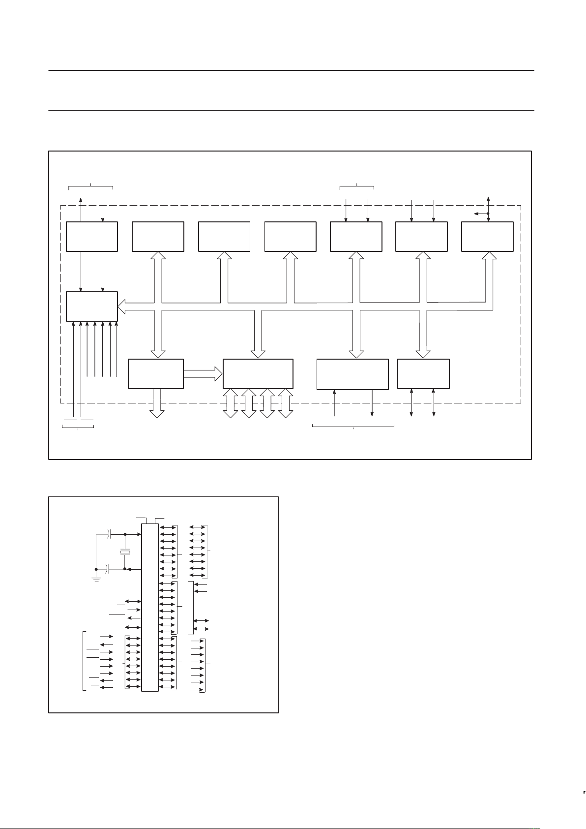
BLOCK DIAGRAM
PROGRAMMABLE I/O
CPU
T0 T1
COUNTERS
XTAL2 XTAL1
INT0
INT1
CONTROL
SERIAL IN SERIAL OUT
OSCILLATOR
AND
TIMING
PROGRAM
MEMORY
(32K x 8
EPROM)
RAM AUX–RAM
DATA
MEMORY
(256 x 8)
TWO 16-BIT
TIMER/EVENT
COUNTERS
DATA
MEMORY
(256 x 8)
16-BIT TIMER/
EVENT COUNTER
WATCHDOG
TIMER
64K-BYTE BUS
EXPANSION
CONTROL
PROGRAMMABLE
SERIAL PORT
FULL DUPLEX UART
SYNCHRONOUS SHIFT
BIT-LEVEL
I
2
C
INTERFACE
FREQUENCY
REFERENCE
T2 T2EX
RST
EXTERNAL
INTERRUPTS
PARALLEL PORTS,
ADDRESS/DATA BUS
AND I/O PINS
SHARED WITH
PORT 3
INTERNAL
INTERRUPTS
SDA SCL
SU00166
LOGIC SYMBOL
PORT 0
PORT 1PORT 2
PORT 3
ADDRESS AND
DATA BUS
ADDRESS BUS
T2
T2EX
RxD
TxD
INT0
INT1
T0
T1
WR
RD
SECONDARY FUNCTIONS
RST
EA
PSEN
ALE
V
SS
V
DD
XTAL1
XTAL2
SCL
SDA
SU00165
Philips Semiconductors Product specification
87C524/87C528
80C51 8-bit microcontrollers
16K/32K, 512 OTP, I
2
C, watchdog timer
1999 Jul 23
4
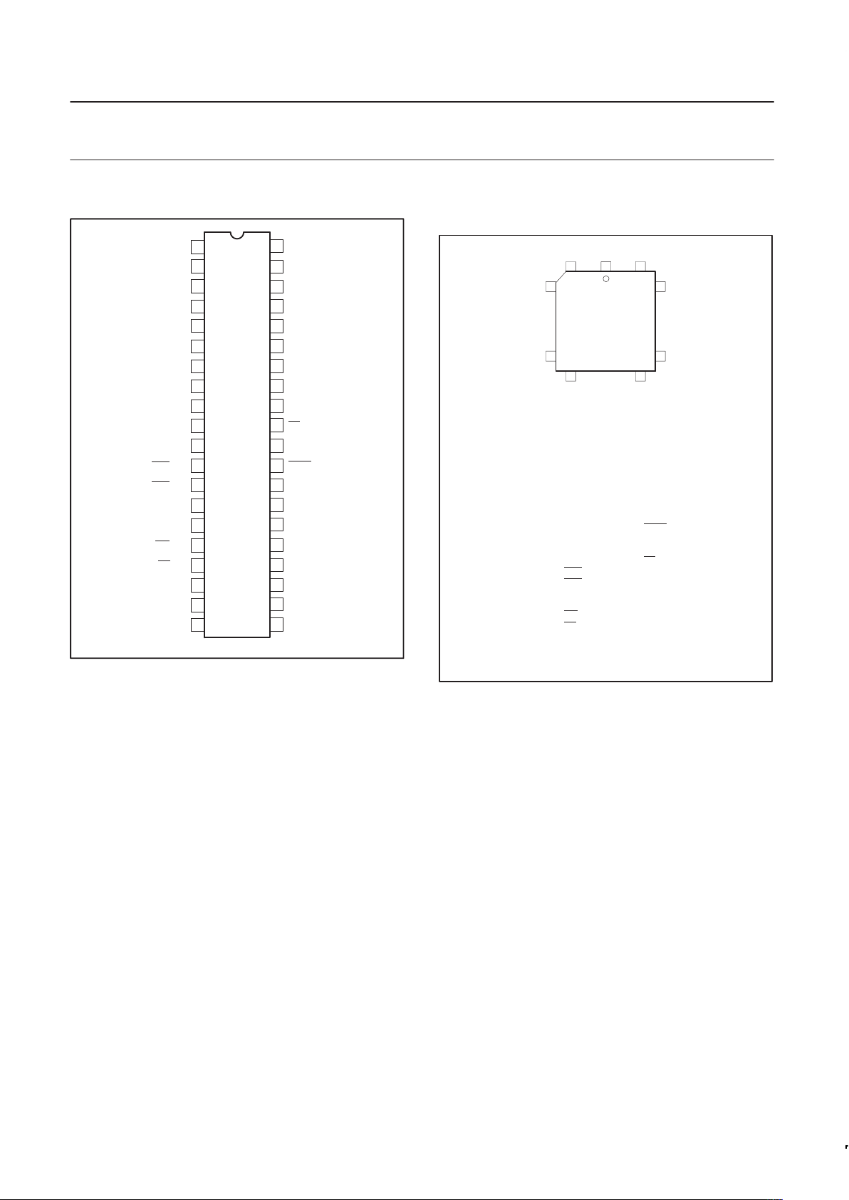
PIN CONFIGURATIONS
1
2
3
4
5
6
7
8
9
10
11
12
13
14
15
16
17
18
19
20
21
22
23
24
25
26
27
28
29
30
31
32
33
34
35
36
37
38
39
40
T2/P1.0
T2EX/P1.1
P1.2
P1.3
P1.4
P1.5
SCL/P1.6
RST
RxD/P3.0
TxD/P3.1
INT0
/P3.2
INT1
/P3.3
T0/P3.4
T1/P3.5
SDA/P1.7
WR
/P3.6
RD
/P3.7
XTAL2
XTAL1
V
SS
P2.0/A8
P2.1/A9
P2.2/A10
P2.3/A11
P2.4/A12
P2.5/A13
P2.6/A14
P2.7/A15
PSEN
ALE
EA
P0.7/AD7
P0.6/AD6
P0.5/AD5
P0.4/AD4
P0.3/AD3
P0.2/AD2
P0.1/AD1
P0.0/AD0
V
DD
DUAL
IN-LINE
PACKAGE
SU00162
PLASTIC LEADED CHIP CARRIER
PIN FUNCTIONS
LCC
6140
7
17
39
29
18 28
Pin Function
1 NC*
2 P1.0/T2
3 P1.1/T2EX
4 P1.2
5 P1.3
6 P1.4
7 P1.5
8 P1.6/SCL
9 P1.7/SDA
10 RST
11 P3.0/RxD
12 NC*
13 P3.1/TxD
14 P3.2/INT0
15 P3.3/INT1
16 P3.4/T0
17 P3.5/T1
18 P3.6/WR
19 P3.7/RD
20 XTAL2
21 XTAL1
22 V
SS
Pin Function
23 NC*
24 P2.0/A8
25 P2.1/A9
26 P2.2/A10
27 P2.3/A11
28 P2.4/A12
29 P2.5/A13
30 P2.6/A14
31 P2.7/A15
32 PSEN
33 ALE
34 NC*
35 EA
36 P0.7/AD7
37 P0.6/AD6
38 P0.5/AD5
39 P0.4/AD4
40 P0.3/AD3
41 P0.2/AD2
42 P0.1/AD1
43 P0.0/AD0
44 V
DD
SU00163A
* NO INTERNAL CONNECTIONS
Philips Semiconductors Product specification
87C524/87C528
80C51 8-bit microcontrollers
16K/32K, 512 OTP, I
2
C, watchdog timer
1999 Jul 23
5
PLASTIC QUAD FLAT PACK
PIN FUNCTIONS
QFP
44 34
1
11
33
23
12 22
Pin Function
1 P1.5
2 P1.6/SCL
3 P1.7/SDA
4 RST
5 P3.0/RxD
6 NC*
7 P3.1/TxD
8 P3.2/INT0
9 P3.3/INT1
10 P3.4/T0
11 P3.5/T1
12 P3.6/WR
13 P3.7/RD
14 XTAL2
15 XTAL1
16 V
SS
17 NC*
18 P2.0/A8
19 P2.1/A9
20 P2.2/A10
21 P2.3/A11
22 P2.4/A12
Pin Function
23 P2.5/A13
24 P2.6/A14
25 P2.7/A15
26 PSEN
27 ALE
28 NC*
29 EA
30 P0.7/AD7
31 P0.6/AD6
32 P0.5/AD5
33 P0.4/AD4
34 P0.3/AD3
35 P0.2/AD2
36 P0.1/AD1
37 P0.0/AD0
38 V
DD
39 NC*
40 P1.0/T2
41 P1.1/T2EX
42 P1.2
43 P1.3
44 P1.4
SU00164
* NO INTERNAL CONNECTIONS
Philips Semiconductors Product specification
87C524/87C528
80C51 8-bit microcontrollers
16K/32K, 512 OTP, I
2
C, watchdog timer
1999 Jul 23
6
PIN DESCRIPTIONS
PIN NO.
MNEMONIC DIP LCC QFP TYPE NAME AND FUNCTION
V
SS
20 22 16 I Ground: circuit ground potential.
V
DD
40 44 38 I Power Supply: +5 V power supply pin during normal operation, Idle mode and
Power-down mode.
P0.0–0.7 39–32 43–36 37–30 I/O Port 0: Port 0 is an open-drain, bidirectional I/O port. Port 0 pins that have 1s written to
them float and can be used as high-impedance inputs. Port 0 is also the multiplexed
low-order address and data bus during accesses to external program and data memory. In
this application, it uses strong internal pull-ups when emitting 1s.
P1.0–P1.7 1–8 2–9 40–44
1–3
I/O Port 1: Port 1 is an 8-bit bidirectional I/O port with internal pull-ups, except P1.6 and P1.7
which have open drain. Port 1 pins that have 1s written to them are pulled high by the
internal pull-ups and can be used as inputs. As inputs, port 1 pins that are externally pulled
low will source current because of the internal pull-ups. (See DC Electrical Characteristics:
I
IL
). Port 1 can sink/source one TTL (4 LSTTL) inputs. Port 1 receives the low-order
address byte during program memory verification. Port 1 also serves alternate functions for
timer 2:
1 2 40 I T2 (P1.0): Timer/counter 2 external count input (following edge triggered).
2 3 41 I T2EX (P1.1): T imer/counter 2 trigger input.
7 8 2 I/O SCL (P1.6): I2C serial port clock line.
8 9 3 I/O SDA (P1.7): I2C serial port data line.
P2.0–P2.7 21–28 24–31 18–25 I/O Port 2: Port 2 is an 8-bit bidirectional I/O port with internal pull-ups. Port 2 pins that have
1s written to them are pulled high by the internal pull-ups and can be used as inputs. As
inputs, port 2 pins that are externally being pulled low will source current because of the
internal pull-ups. (See DC Electrical Characteristics: I
IL
). Port 2 emits the high-order
address byte during fetches from external program memory and during accesses to
external data memory that use 16-bit addresses (MOVX @DPTR). In this application, it
uses strong internal pull-ups when emitting 1s. During accesses to external data memory
that use 8-bit addresses (MOV @Ri), port 2 emits the contents of the P2 special function
register.
P3.0–P3.7 10–17 11,
13–19
5,
7–13
I/O Port 3: Port 3 is an 8-bit bidirectional I/O port with internal pull-ups. Port 3 pins that have
1s written to them are pulled high by the internal pull-ups and can be used as inputs. As
inputs, port 3 pins that are externally being pulled low will source current because of the
pull-ups. (See DC Electrical Characteristics: I
IL
). Port 3 also serves the special features of
the SC80C51 family, as listed below:
10 11 5 I RxD (P3.0): Serial input port
11 13 7 O TxD (P3.1): Serial output port
12 14 8 I INT0 (P3.2): External interrupt
13 15 9 I INT1 (P3.3): External interrupt
14 16 10 I T0 (P3.4): Timer 0 external input
15 17 11 I T1 (P3.5): Timer 1 external input
16 18 12 O WR (P3.6): External data memory write strobe
17 19 13 O RD (P3.7): External data memory read strobe
RST 9 10 4 I/O Reset: A high on this pin for two machine cycles while the oscillator is running, resets the
device. An internal diffused resistor to V
SS
permits a power-on reset using only an external
capacitor to V
DD
. After a watchdog timer overflow, this pin is pulled high while the internal
reset signal is active.
ALE 30 33 27 I/O Address Latch Enable: Output pulse for latching the low byte of the address during an
access to external memory. In normal operation, ALE is emitted at a constant rate of 1/6
the oscillator frequency, and can be used for external timing or clocking. Note that one ALE
pulse is skipped during each access to external data memory.
PSEN 29 32 26 O Program Store Enable: The read strobe to external program memory. When the device is
executing code from the external program memory, PSEN
is activated twice each machine
cycle, except that two PSEN
activations are skipped during each access to external data
memory. PSEN
is not activated during fetches from internal program memory.
EA 31 35 29 I External Access Enable: EA must be externally held low during RESET to enable the
device to fetch code from external program memory locations 0000H to 7FFFH. If EA
is
held high during RESET, the device executes from internal program memory unless the
program counter contains an address greater than 7FFFH. EA
is don’t care after RESET.
XTAL1 19 21 15 I Crystal 1: Input to the inverting oscillator amplifier and input to the internal clock generator
circuits.
XTAL2 18 20 14 O Crystal 2: Output from the inverting oscillator amplifier .
Philips Semiconductors Product specification
87C524/87C528
80C51 8-bit microcontrollers
16K/32K, 512 OTP, I
2
C, watchdog timer
1999 Jul 23
7
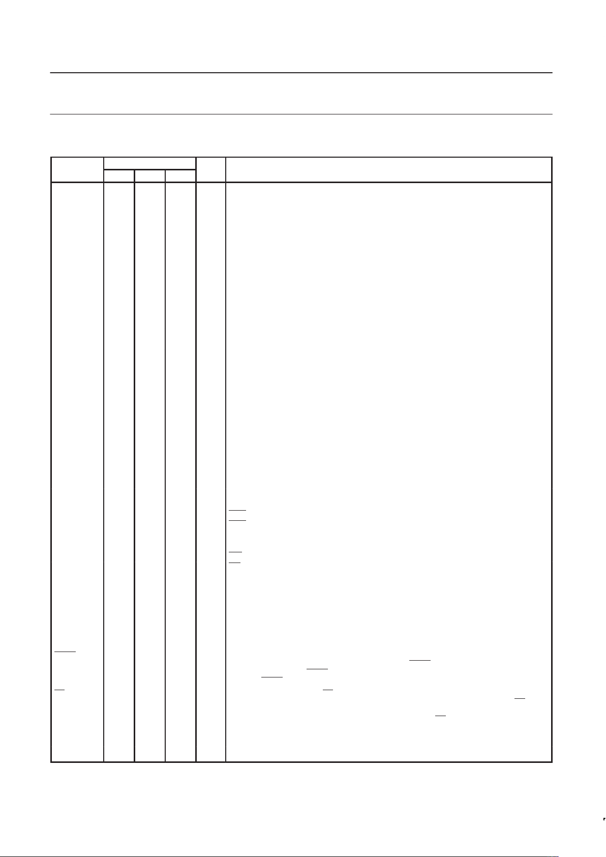
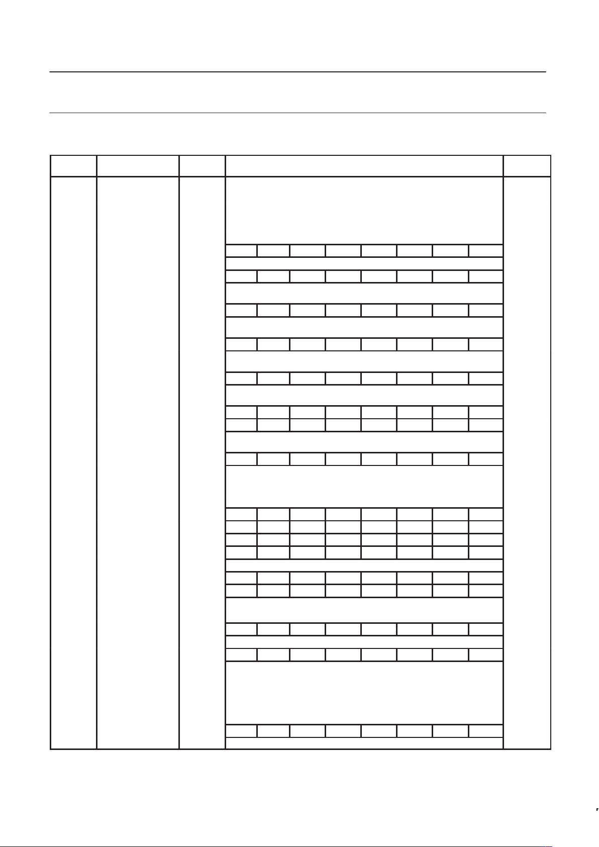
Table 1. 8XC524/8XC528 Special Function Registers
SYMBOL DESCRIPTION
DIRECT
ADDRESS
BIT ADDRESS, SYMBOL, OR ALTERNATIVE PORT FUNCTION
MSB LSB
RESET
VALUE
ACC* Accumulator E0H E7 E6 E5 E4 E3 E2 E1 E0 00H
B* B register F0H F7 F6 F5 F4 F3 F2 F1 F0 00H
DPTR:
DPH
DPL
Data pointer (2 bytes):
Data pointer high
Data pointer low
83H
82H
00H
00H
AF AE AD AC AB AA A9 A8
IE*# Interrupt enable A8H EA ES1 ET2 ES0 ET1 EX1 ET0 EX0 00H
BF BE BD BC BB BA B9 B8
IP*# Interrupt priority B8H – PS1 PT2 PS0 PT1 PX1 PT0 PX0 x0000000B
87 86 85 84 83 82 81 80
P0* Port 0 80H AD7 AD6 AD5 AD4 AD3 AD2 AD1 AD0 FFH
97 96 95 94 93 92 91 90
P1* Port 1 90H SDA SEL – – – – T2EX T2 FFH
A7 A6 A5 A4 A3 A2 A1 A0
P2* Port 2 A0H A15 A14 A13 A12 A11 A10 A9 A8 FFH
B7 B6 B5 B4 B3 B2 B1 B0
P3* Port 3 B0H RD WR T1 T0 INT1 INT0 TxD RxD FFH
PCON Power control 87H SMOD – – – GF1 GF0 PD IDL 0xxx0000B
D7 D6 D5 D4 D3 D2 D1 D0
PSW* Program status word D0H CY AC F0 RS1 RS0 OV F1 P 00H
RCAP2H#
RCAP2L#
SBUF
Capture high
Capture low
Serial data buffer
CBH
CAH
99H
00H
00H
xxxxxxxxB
9F 9E 9D 9C 9B 9A 99 98
SCON* Serial controller 98H SM0 SM1 SM2 REN TB8 RB8 TI RI 00H
S1BIT# Serial I2C data D9H/RD SDI 0 0 0 0 0 0 0 x0000000B
WR SD0 X X X X X X X 0xxxxxxxB
S1INT# Serial I2C interrupt DAH INT X X X X X X X 0xxxxxxxB
DF DE DD DC DB DA D9 D8
S1SCS*# Serial I2C control D8H/RD SDI SCI CLH BB RBF WBF STR ENS xxxx0000B
WR SD0 SC0 CLH X X X STR ENS 00xxxx00B
SP Stack pointer 81H 07H
8F 8E 8D 8C 8B 8A 89 88
TCON* Timer control 88H TF1 TR1 TF0 TR0 IE1 IT1 IE0 IT0 00H
CF CE CD CC CB CA C9 C8
T2CON*# Timer 2 control C8H TF2 EXF2 RCLK TCLK EXEN2 TR2 C/T2
CP/RL2
00H
TH0
TH1
TH2#
TL0
TL1
TL2#
T3#
Timer high 0
Timer high 1
Timer high 2
Timer low 0
Timer low 1
Timer low 2
Watchdog timer
8CH
8DH
CDH
8AH
8BH
CCH
FFH
00H
00H
00H
00H
00H
00H
00H
TMOD Timer mode 89H GATE C/T M1 M0 GATE C/T M1 M0 00H
WDCON# Watchdog control A5H A5H
* SFRs are bit addressable.
# SFRs are modified from or added to the 80C51 SFRs.

Philips Semiconductors Product specification
87C524/87C528
80C51 8-bit microcontrollers
16K/32K, 512 OTP, I
2
C, watchdog timer
1999 Jul 23
8
Table 2. Internal and External Program Memory Access with Security Bit Set
INSTRUCTION
ACCESS TO INTERNAL
PROGRAM MEMORY
ACCESS TO EXTERNAL
PROGRAM MEMORY
MOVC in internal program memory YES YES
MOVC in external program memory NO YES
INTERNAL DATA MEMORY
The internal data memory is divided into three physically separated
segments: 256 bytes of RAM, 256 bytes of AUX-RAM, and a
128 bytes special function area. These can be addressed each in a
different way .
– RAM 0 to 127 can be addressed directly and indirectly as in the
80C51. Address pointers are R0 and R1 of the selected register
bank.
– RAM 128 to 255 can only be addressed indirectly as in the 80C51.
Address pointers are R0 and R1 of the selected register bank.
– AUX-RAM 0 to 255 is indirectly addressed in the same way as
external data memory with the MOVX instructions. Address
pointers are R0, R1 of the selected register bank and DPTR. An
access to AUX-RAM 0 to 255 will not affect ports P0, P2, P3.6
and P3.7.
An access to external data memory locations higher than 255 will be
performed with the MOVX DPTR instructions in the same way as in
the 8051 structure, so with P0 and P2 as data/address bus and P3.6
and P3.7 as write and read timing signals. Note that these external
data memory cannot be accessed with R0 and R1 as address
pointer.
TIMER 2
Timer 2 is functionally equal to the Timer 2 of the 8052AH. Timer 2 is
a 16-bit timer/counter. These 16 bits are formed by two special
function registers TL2 and TH2. Another pair of special function
register RCAP2L and RCAP2H form a 16-bit capture register or a
16-bit reload register. Like Timer 0 and 1, it can operate either as a
timer or as an event counter. This is selected by bit C/T2N in the
special function register T2CON. It has three operating modes:
capture, autoload, and baud rate generator mode which are selected
by bits in T2CON.
WATCHDOG TIMER T3
The watchdog timer consists of an 11-bit prescaler and an 8-bit timer
formed by special function register T3. The prescaler is incremented
by an on-chip oscillator with a fixed frequency of 1MHz. The
maximum tolerance on this frequency is –50% and +100%. The 8-bit
timer increments every 2048 cycles of the on-chip oscillator. When a
timer overflow occurs, the microcontroller is reset and a reset output
pulse of 16 × 2048 cycles of the on-chip oscillator is generated at pin
RST. The internal RESET signal is not inhibited when the external
RST pin is kept low by, for example, an external reset circuit. The
RESET signal drives port 1, 2, 3 into the high state and port 0 into
the high impedance state.
The watchdog timer is controlled by one special function register
WDCON with the direct address location A5H. WDCON can be read
and written by software. A value of A5H in WDCON halts the
on-chip oscillator and clears both the prescaler and timer T3. After
the RESET signal, WDCON contains A5H. Every value other than
A5H in WDCON enables the watchdog timer. When the watchdog
timer is enabled, it runs independently of the XTAL-clock.
Timer T3 can be read on the fly. Timer T3 can only be written if
WDCON contains the value 5AH. A successful write operation to T3
will clear the prescaler and WDCON, leaving the watchdog enabled
and preventing inadvertent changes of T3. To prevent an overflow of
the watchdog timer, the user program has to reload the watchdog
timer within periods that are shorter than the programmed watchdog
timer internal. This time interval is determined by an 8-bit value that
has to be loaded in register T3 while at the same time the prescaler
is cleared by hardware.
Watchdog timer interval =
[256 * (T3)] 2048
on * chip oscillator frequency
BIT-LEVEL I2C INTERFACE
This bit-level serial I/O interface supports the I2C-bus. P1.6/SCL and
P1.7/SDA are the serial I/O pins. These two pins meet the I
2
C
specification concerning the input levels and output drive capability.
Consequently , these pins have an open drain output configuration.
All the four modes of the I
2
C-bus are supported:
– master transmitter
– master receiver
– slave transmitter
– slave receiver
The advantages of the bit-level I
2
C hardware compared with a full
software I
2
C implementation are:
– the hardware can generate the SCL pulse
– Testing a single bit (RBF respectively, WBF) is sufficient as a
check for error free transmission.
The bit-level I
2
C hardware operates on serial bit level and performs
the following functions:
– filtering the incoming serial data and clock signals
– recognizing the START condition
– generating a serial interrupt request SI after reception of a START
condition and the first falling edge of the serial clock
– recognizing the STOP condition
– recognizing a serial clock pulse on the SCL line
– latching a serial bit on the SDA line (SDI)
– stretching the SCL LOW period of the serial clock to suspend the
transfer of the next serial data bit
– setting Read Bit Finished (RBF) when the SCL clock pulse has
finished and Write Bit Finished (WBF) if there is no arbitration loss
detected (i.e., SDA = 0 while SDO = 1)
– setting a serial clock Low-to-High detected (CLH) flag
– setting a Bus Busy (BB) flag on a START condition and clearing
this flag on a STOP condition
– releasing the SCL line and clearing the CLH, RBF and WBF flags
to resume transfer of the next serial data bit
– generating an automatic clock if the single bit data register S1BIT
is used in master mode.
The following functions must be done in software:
– handling the I
2
C START interrupts
– converting serial to parallel data when receiving
– converting parallel to serial data when transmitting
– comparing the received slave address with its own
– interpreting the acknowledge information
– guarding the I
2
C status if RBF or WBF = 0.
 Loading...