


|
|
|
|
|
|
|
|
|
|
|
|
|
|
|
|
|
|
|
|
P89C660 |
INTEGRATED CIRCUITS |
||||||||||||||||||
|
|
|
|
|
|
|
|
|
|
|
|
|
|
|
|
|
|
|
|
|
|
|
|
|
|
|
|
|
|
|
|
|
|
|
|
|
|
|
|
|
|
|
|
|
|
|
|
|
|
|
|
|
|
|
|
|
|
|
|
|
|
|
|
|
|
|
|
|
|
|
|
|
|
|
|
|
|
|
|
|
|
|
|
|
|
|
|
|
|
|
|
|
|
|
|
|
|
|
|
|
|
|
|
|
|
|
|
|
|
|
|
|
|
|
|
|
|
|
|
P89C660/P89C662/P89C664/P89C668
80C51 8-bit Flash microcontroller family
16KB/32KB/64KB ISP/IAP FLASH with 512B/1KB/2KB/8KB RAM
Product data
Replaces P89C660/P89C662/P89C664 of 2001 Jul 19 |
2002 Oct 28 |
and P89C668 of 2001 Jul 27 |
|
P s
on o s

Philips Semiconductors Product data
80C51 8-bit Flash microcontroller family |
P89C660/P89C662/P89C664/ |
16KB/32KB/64KB ISP/IAP Flash with 512B/1KB/2KB/8KB RAM |
P89C668 |
|
|
|
|
DESCRIPTION
The P89C660/662/664/668 device contains a non-volatile 16KB/32KB/64KB Flash program memory that is both parallel programmable and serial In-System and In-Application Programmable. In-System Programming (ISP) allows the user to download new code while the microcontroller sits in the application. In-Application Programming (IAP) means that the microcontroller fetches new program code and reprograms itself while in the system. This allows for remote programming over a modem link.
A default serial loader (boot loader) program in ROM allows serial
In-System Programming of the Flash memory via the UART without the need for a loader in the Flash code. For In-Application Programming, the user program erases and reprograms the Flash memory by use of standard routines contained in ROM.
This device executes one instruction in 6 clock cycles, hence providing twice the speed of a conventional 80C51. An OTP configuration bit gives the user the option to select conventional 12-clock timing.
This device is a Single-Chip 8-Bit Microcontroller manufactured in advanced CMOS process and is a derivative of the 80C51 microcontroller family. The instruction set is 100% executing and timing compatible with the 80C51 instruction set.
The device also has four 8-bit I/O ports, three 16-bit timer/event counters, a multi-source, four-priority-level, nested interrupt structure, an enhanced UART and on-chip oscillator and timing circuits.
The added features of the P89C660/662/664/668 makes it a powerful microcontroller for applications that require pulse width modulation, high-speed I/O and up/down counting capabilities such as motor control.
FEATURES
•80C51 Central Processing Unit
•On-chip Flash program memory with In-System Programming
(ISP) and In-Application Programming (IAP) capability
•Boot ROM contains low level Flash programming routines for downloading via the UART
•Can be programmed by the end-user application (IAP)
•Parallel programming with 87C51 compatible hardware interface to programmer
•Six clocks per machine cycle operation (standard)
•12 clocks per machine cycle operation (optional)
•Speed up to 20 MHz with 6 clock cycles per machine cycle
(40 MHz equivalent performance); up to 33 MHz with 12 clocks per machine cycle
•Fully static operation
•RAM externally expandable to 64 kbytes
•Four interrupt priority levels
•Eight interrupt sources
•Four 8-bit I/O ports
•Full-duplex enhanced UART
±Framing error detection
±Automatic address recognition
•Power control modes
±Clock can be stopped and resumed
±Idle mode
±Power-Down mode
•Programmable clock out
•Second DPTR register
•Asynchronous port reset
•Low EMI (inhibit ALE)
•I2C serial interface
•Programmable Counter Array (PCA)
±PWM
±Capture/compare
•Well-suited for IPMI applications
2002 Oct 28 |
2 |
853-2392 29118 |

Philips Semiconductors Product data
80C51 8-bit Flash microcontroller family |
P89C660/P89C662/P89C664/ |
16KB/32KB/64KB ISP/IAP Flash with 512B/1KB/2KB/8KB RAM |
P89C668 |
|
|
SELECTION TABLE |
|
Type |
|
Memory |
|
|
Timers |
|
Serial Inter- |
|
|
|
|
|
|
|
|
|||||
|
|
|
|
|
faces |
|
|
|
|
|
|
|
|
|||||||
|
|
|
|
|
|
|
|
|
|
|
|
|
|
|
|
|
|
|||
|
|
|
|
|
|
|
|
|
|
|
|
|
|
ADC bits/ch. |
|
|
|
Default Clock Rate |
Optional Clock Rate |
Reset active low/high? |
|
RAM |
ROM |
OTP |
Flash |
# of Timers |
PWM |
PCA |
WD |
UART |
I 2C |
CAN |
|
SPI |
I/O Pins |
Interrupts (External) |
Program Security |
||||
P89C668 |
8K |
± |
± |
64K |
4 |
√ |
√ |
√ |
√ |
√ |
± |
|
± |
± |
32 |
8(2)/4 |
√ |
6-clk |
12-clk |
H |
P89C664 |
2K |
± |
± |
64K |
4 |
√ |
√ |
√ |
√ |
√ |
± |
|
± |
± |
32 |
8(2)/4 |
√ |
6-clk |
12-clk |
H |
P89C662 |
1K |
± |
± |
32K |
4 |
√ |
√ |
√ |
√ |
√ |
± |
|
± |
± |
32 |
8(2)/4 |
√ |
6-clk |
12-clk |
H |
P89C660 |
512B |
± |
± |
16K |
4 |
√ |
√ |
√ |
√ |
√ |
± |
|
± |
± |
32 |
8(2)/4 |
√ |
6-clk |
12-clk |
H |
|
|
|
|
|
|
|
|
|
|
|
|
|
|
|
|
|
|
|
|
|
Max. |
Freq. |
Freq. |
||
Freq. |
||||
Range |
Range |
|||
at 6-clk |
||||
at |
3V |
at 5V |
||
/ 12-clk |
||||
(MHz) |
(MHz) |
|||
(MHz) |
||||
|
|
|
||
20/33 |
|
± |
0-20/33 |
|
20/33 |
|
± |
0-20/33 |
|
20/33 |
|
± |
0-20/33 |
|
20/33 |
|
± |
0-20/33 |
|
|
|
|
|
|
ORDERING INFORMATION
|
MEMORY |
TEMPERATURE RANGE (°C) |
VOLTAGE |
FREQUENCY (MHz) |
|
|||
DEVICE |
|
|
|
|
DWG # |
|||
FLASH |
RAM |
6 CLOCK MODE |
12 CLOCK |
|||||
AND PACKAGE |
RANGE |
|||||||
|
|
|||||||
|
|
|
|
MODE |
|
|||
|
|
|
|
|
|
|
||
|
|
|
|
|
|
|
|
|
P89C660HBA |
16 KB |
512 B |
0 to +70, PLCC |
4.5±5.5 V |
0 to 20 MHz |
0 to 33 MHz |
SOT187-2 |
|
|
|
|
|
|
|
|
|
|
P89C660HFA |
16 KB |
512 B |
±40 to +85, PLCC |
4.75±5.25 V |
0 to 20 MHz |
0 to 33 MHz |
SOT187-2 |
|
|
|
|
|
|
|
|
|
|
P89C660HBBD |
16 KB |
512 B |
0 to +70, LQFP |
4.5±5.5 V |
0 to 20 MHz |
0 to 33 MHz |
SOT389-1 |
|
|
|
|
|
|
|
|
|
|
P89C662HBA |
32 KB |
1 KB |
0 to +70, PLCC |
4.5±5.5 V |
0 to 20 MHz |
0 to 33 MHz |
SOT187-2 |
|
|
|
|
|
|
|
|
|
|
P89C662HFA |
32 KB |
1 KB |
±40 to +85, PLCC |
4.75±5.25 V |
0 to 20 MHz |
0 to 33 MHz |
SOT187-2 |
|
|
|
|
|
|
|
|
|
|
P89C662HBBD |
32 KB |
1 KB |
0 to +70, LQFP |
4.5±5.5 V |
0 to 20 MHz |
0 to 33 MHz |
SOT389-1 |
|
|
|
|
|
|
|
|
|
|
P89C662HFBD |
32 KB |
1 KB |
±40 to +85, LQFP |
4.75±5.25 V |
0 to 20 MHz |
0 to 33 MHz |
SOT389-1 |
|
|
|
|
|
|
|
|
|
|
P89C664HBA |
64 KB |
2 KB |
0 to +70, PLCC |
4.5±5.5 V |
0 to 20 MHz |
0 to 33 MHz |
SOT187-2 |
|
|
|
|
|
|
|
|
|
|
P89C664HFA |
64 KB |
2 KB |
±40 to +85, PLCC |
4.75±5.25 V |
0 to 20 MHz |
0 to 33 MHz |
SOT187-2 |
|
|
|
|
|
|
|
|
|
|
P89C664HBBD |
64 KB |
2 KB |
0 to +70, LQFP |
4.5±5.5 V |
0 to 20 MHz |
0 to 33 MHz |
SOT389-1 |
|
|
|
|
|
|
|
|
|
|
P89C664HFBD |
64 KB |
2 KB |
±40 to +85, LQFP |
4.75±5.25 V |
0 to 20 MHz |
0 to 33 MHz |
SOT389-1 |
|
|
|
|
|
|
|
|
|
|
P89C668HBA |
64 KB |
8 KB |
0 to +70, PLCC |
4.5±5.5 V |
0 to 20 MHz |
0 to 33 MHz |
SOT187-2 |
|
|
|
|
|
|
|
|
|
|
P89C668HFA |
64 KB |
8 KB |
±40 to +85, PLCC |
4.5±5.5 V |
0 to 20 MHz |
0 to 33 MHz |
SOT187-2 |
|
|
|
|
|
|
|
|
|
|
P89C668HBBD |
64 KB |
8 KB |
0 to +70, LQFP |
4.5±5.5 V |
0 to 20 MHz |
0 to 33 MHz |
SOT389-1 |
|
|
|
|
|
|
|
|
|
|
2002 Oct 28 |
3 |
Philips Semiconductors Product data
80C51 8-bit Flash microcontroller family |
P89C660/P89C662/P89C664/ |
16KB/32KB/64KB ISP/IAP Flash with 512B/1KB/2KB/8KB RAM |
P89C668 |
|
|
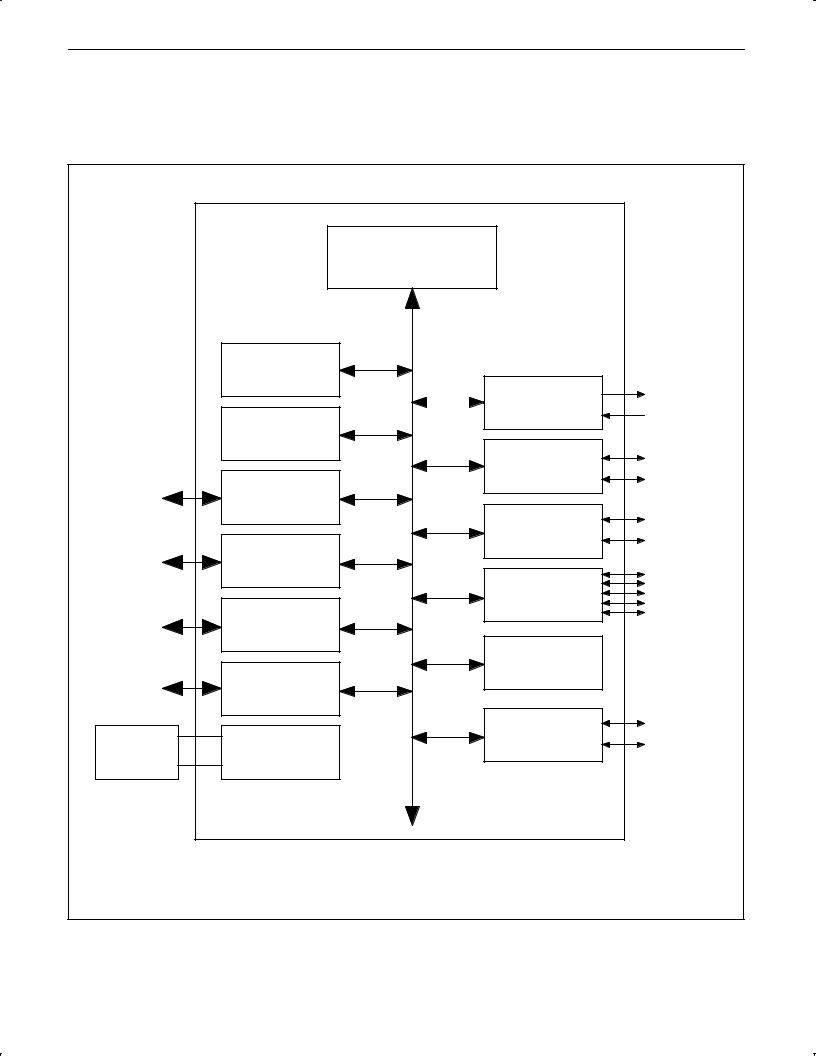
BLOCK DIAGRAM 1
|
|
ACCELERATED 80C51 CPU |
|
|
6-CLK MODE (DEFAULT) |
|
|
12-CLK MODE (OPTIONAL) |
|
16K / 32K / |
|
|
64 KBYTE |
|
|
CODE FLASH |
|
|
|
FULL-DUPLEX |
|
|
ENHANCED UART |
|
0.5K / 1K / 2K / |
|
|
8 KBYTE DATA RAM |
|
|
|
TIMER 0 |
|
|
TIMER 1 |
|
PORT 3 |
|
|
CONFIGURABLE I/Os |
|
|
|
TIMER 2 |
|
PORT 2 |
|
|
CONFIGURABLE I/Os |
|
|
|
PROGRAMMABLE |
|
|
COUNTER ARRAY |
|
PORT 1 |
(PCA) |
|
|
|
|
CONFIGURABLE I/Os |
|
|
|
WATCHDOG TIMER |
|
PORT 0 |
|
|
CONFIGURABLE I/Os |
|
|
|
I2C |
CRYSTAL OR |
OSCILLATOR |
INTERFACE |
|
||
RESONATOR |
|
|
|
|
su01713 |
2002 Oct 28 |
|
4 |

Philips Semiconductors Product data
80C51 8-bit Flash microcontroller family |
P89C660/P89C662/P89C664/ |
16KB/32KB/64KB ISP/IAP Flash with 512B/1KB/2KB/8KB RAM |
P89C668 |
|
|
BLOCK DIAGRAM (CPU-ORIENTED)
|
|
|
|
P0.0±P0.7 |
P2.0±P2.7 |
|
|
|
|
|
|
PORT 0 |
PORT 2 |
|
|
|
|
|
|
DRIVERS |
DRIVERS |
|
|
VCC |
|
|
|
|
|
|
|
VSS |
|
|
|
|
|
|
|
|
RAM ADDR |
RAM |
PORT 0 |
PORT 2 |
FLASH |
|
|
|
REGISTER |
|
LATCH |
LATCH |
|
|
|
|
|
|
|
|
|
|
8 |
|
B |
|
ACC |
|
|
STACK |
|
|
REGISTER |
|
|
|
POINTER |
|
|
|
|
|
|
|
|
||
|
|
|
|
|
|
|
PROGRAM |
|
|
|
|
|
TMP1 |
|
ADDRESS |
|
|
|
|
TMP2 |
|
REGISTER |
|
|
|
|
|
ALU |
|
|
BUFFER |
|
|
|
|
|
|
|
|
|
|
|
|
|
SFRs |
|
|
|
|
|
|
|
TIMERS |
|
PC |
|
|
|
|
PSW |
P.C.A. |
|
INCRE- |
|
|
|
|
|
|
MENTER |
|
|
|
|
|
|
|
|
|
|
|
|
|
|
|
8 |
16 |
|
|
|
|
|
|
|
PROGRAM |
|
|
|
|
|
|
|
COUNTER |
PSEN |
|
INSTRUCTION |
REGISTER |
|
|
|
|
ALE |
TIMING |
|
|
|
DPTR'S |
||
EA/VPP |
AND |
|
|
|
MULTIPLE |
||
CONTROL |
|
|
|
|
|||
RST |
|
|
|
|
|
||
|
PD |
|
|
PORT 1 |
I2C |
PORT 3 |
|
|
|
|
|
LATCH |
|
LATCH |
|
|
OSCILLATOR |
|
|
|
|
||
|
|
|
|
PORT 1 |
|
PORT 3 |
|
|
|
|
|
DRIVERS |
|
DRIVERS |
|
|
XTAL1 |
|
XTAL2 |
SCL |
|
|
|
|
|
|
|
|
|
||
|
|
|
|
P1.0±P1.7 |
SDA |
P3.0±P3.7 |
|
|
|
|
|
|
|
||
|
|
|
|
|
|
|
su01089 |
2002 Oct 28 |
|
|
|
|
5 |
|
|
Philips Semiconductors Product data
80C51 8-bit Flash microcontroller family |
P89C660/P89C662/P89C664/ |
16KB/32KB/64KB ISP/IAP Flash with 512B/1KB/2KB/8KB RAM |
P89C668 |
|
|
LOGIC SYMBOL |
|
|
|
|
|
||
|
|
VCC |
VSS |
|
|
|
|
|
|
XTAL1 |
|
|
|
|
|
|
|
|
|
0 |
ADDRESS AND |
|
|
|
|
|
|
PORT |
DATA BUS |
|
|
|
|
|
|
|
|
|
|
|
|
XTAL2 |
|
|
|
|
|
|
|
|
|
|
T2 |
|
|
|
|
|
|
1 |
T2EX |
|
|
|
|
RST |
|
|
|
|
|
|
|
|
PORT |
|
|
|
|
|
|
EA/VPP |
|
|
|
|
|
|
|
|
|
|
|
|
|
|
|
PSEN |
|
|
|
|
|
FUNCTIONSSECONDARY |
ALE/PROG |
|
|
SCL |
|
|
|
|
2PORT |
SDA |
|
|
|||
RxD |
3PORT |
|
|
|
|||
|
|
|
|
|
|
||
|
|
|
|
|
|
|
|
|
TxD |
|
|
|
|
|
|
|
INT0 |
|
|
|
|
|
|
|
INT1 |
|
|
|
ADDRESS BUS |
|
|
|
T0 |
|
|
|
|
|
|
|
|
|
|
|
|
|
|
|
T1 |
|
|
|
|
|
|
|
WR |
|
|
|
|
|
|
|
RD |
|
|
|
|
|
|
|
|
|
|
|
SU01090 |
|
|
PINNING |
|
|
|
|
|
|
|
Plastic Leaded Chip Carrier |
|
|
Low Quad Flat Pack |
|
|||
|
|
6 |
1 |
40 |
|
44 |
34 |
|
|
|
|
|
|||
|
|
7 |
|
|
39 |
1 |
33 |
|
|
|
PLCC |
|
|
|
LQFP |
|
|
17 |
|
|
|
11 |
23 |
|
|
|
|
29 |
|
|
|
|
|
18 |
|
28 |
|
12 |
22 |
Pin |
Function |
Pin |
Function |
Pin |
Function |
Pin |
Function |
Pin |
Function |
Pin |
Function |
|||||||||||||
1 |
P1.5/CEX2 |
16 |
VSS |
31 |
P0.6/AD6 |
|||||||||||||||||||
1 |
NIC* |
16 |
P3.4/T0/CEX3 |
31 |
P2.7/A15 |
|||||||||||||||||||
2 |
P1.6/SCL |
17 |
NIC* |
32 |
P0.5/AD5 |
|||||||||||||||||||
|
|
|
|
|
|
|
|
|
|
|
|
|||||||||||||
2 |
P1.0/T2 |
17 |
P3.5/T1/CEX4 |
32 |
PSEN |
|||||||||||||||||||
3 |
P1.7/SDA |
18 |
P2.0/A8 |
33 |
P0.4/AD4 |
|||||||||||||||||||
|
|
|
|
|
|
|
|
33 |
ALE |
|||||||||||||||
3 |
P1.1/T2EX |
18 |
P3.6/WR |
4 |
RST |
19 |
P2.1/A9 |
34 |
P0.3/AD3 |
|||||||||||||||
|
|
|
|
|
|
|
|
34 |
NIC* |
|||||||||||||||
4 |
P1.2/ECI |
19 |
P3.7/RD |
|||||||||||||||||||||
5 |
P3.0/RxD |
20 |
P2.2/A10 |
35 |
P0.2/AD2 |
|||||||||||||||||||
|
|
|
|
|
|
|
|
|
|
|
|
|||||||||||||
5 |
P1.3/CEX0 |
20 |
XTAL2 |
35 |
EA/VPP |
|||||||||||||||||||
6 |
NIC* |
21 |
P2.3/A11 |
36 |
P0.1/AD1 |
|||||||||||||||||||
6 |
P1.4/CEX1 |
21 |
XTAL1 |
36 |
P0.7/AD7 |
|||||||||||||||||||
7 |
P3.1/TxD |
22 |
P2.4/A12 |
37 |
P0.0/AD0 |
|||||||||||||||||||
7 |
P1.5/CEX2 |
22 |
VSS |
37 |
P0.6/AD6 |
|||||||||||||||||||
|
|
|
|
|
|
23 |
P2.5/A13 |
38 |
VCC |
|||||||||||||||
8 |
P3.2/INT0 |
|||||||||||||||||||||||
8 |
P1.6/SCL |
23 |
NIC* |
38 |
P0.5/AD5 |
|||||||||||||||||||
|
|
|
|
|
|
24 |
P2.6/A14 |
39 |
NIC* |
|||||||||||||||
9 |
P1.7/SDA |
24 |
P2.0/A8 |
39 |
P0.4/AD4 |
9 |
P3.3/INT1 |
|||||||||||||||||
10 |
P3.4/T0/CEX3 |
25 |
P2.7/A15 |
40 |
P1.0/T2 |
|||||||||||||||||||
10 |
RST |
25 |
P2.1/A9 |
40 |
P0.3/AD3 |
|||||||||||||||||||
|
|
|
|
|
|
|
|
|
|
41 |
P1.1/T2EX |
|||||||||||||
11 |
P3.0/RxD |
26 |
P2.2/A10 |
41 |
P0.2/AD2 |
11 |
P3.5/T1/CEX4 |
26 |
PSEN |
|||||||||||||||
|
|
|
|
|
|
|
|
|
|
42 |
P1.2/ECI |
|||||||||||||
12 |
NIC* |
27 |
P2.3/A11 |
42 |
P0.1/AD1 |
12 |
P3.6/WR |
27 |
ALE |
|||||||||||||||
|
|
|
|
|
|
|
|
|
|
43 |
P1.3/CEX0 |
|||||||||||||
13 |
P3.1/TxD |
28 |
P2.4/A12 |
43 |
P0.0/AD0 |
13 |
P3.7/RD |
28 |
NIC* |
|||||||||||||||
|
|
|
|
|
|
|
|
|
|
44 |
P1.4/CEX1 |
|||||||||||||
14 |
XTAL2 |
29 |
EA/VPP |
|||||||||||||||||||||
14 |
|
|
|
29 |
P2.5/A13 |
44 |
VCC |
|||||||||||||||||
P3.2/INT0 |
|
|
|
|||||||||||||||||||||
|
|
|
|
|
|
|
|
|
|
|
|
15 |
XTAL1 |
30 |
P0.7/AD7 |
|
|
|||||||
15 |
P3.3/INT1 |
30 |
P2.6/A14 |
|
|
|
|
|
|
|||||||||||||||
|
|
|
|
|
|
|
|
|
|
|
|
|
|
|
|
|||||||||
* NO INTERNAL CONNECTION |
|
|
|
|
|
|
|
* NO INTERNAL CONNECTION |
|
|
|
|
SU01401 |
|||||||||||
|
|
|
|
|
SU01091 |
|
|
|
|
|
|
|
|
|
|
|
||||||||
|
|
|
|
|
|
|
|
|
|
|
|
|
|
|
|
|
||||||||
|
|
|
|
|
|
|
|
|
|
|
|
|
|
|
|
|
|
|
|
|
|
|||
2002 Oct 28 |
6 |

Philips Semiconductors Product data
|
80C51 8-bit Flash microcontroller family |
|
P89C660/P89C662/P89C664/ |
||||||||||||||||
|
16KB/32KB/64KB ISP/IAP Flash with 512B/1KB/2KB/8KB RAM |
|
|
P89C668 |
|||||||||||||||
|
|
|
|
|
|
|
|
|
|
|
|
|
|
|
|
|
|
|
|
PIN DESCRIPTIONS |
|
|
|
|
|
|
|
|
|
|
|
|
|
|
|
||||
|
|
|
|
|
|
|
|
|
|
|
|
|
|
|
|
|
|
|
|
|
MNEMONIC |
PIN NUMBER |
TYPE |
|
|
|
|
|
|
|
|
NAME AND FUNCTION |
|||||||
|
|
|
|
|
|
|
|
|
|
|
|
||||||||
PLCC |
|
LQFP |
|
|
|
|
|
|
|
|
|||||||||
|
|
|
|
|
|
|
|
|
|
|
|
|
|
|
|
|
|
||
|
|
|
|
|
|
|
|
|
|
|
|
|
|
|
|
|
|
|
|
|
VSS |
22 |
|
16 |
I |
Ground: 0 V reference. |
|
|
|
|
|
||||||||
|
VCC |
44 |
|
38 |
I |
Power Supply: This is the power supply voltage for normal, idle, and power-down operation. |
|||||||||||||
|
P0.0±0.7 |
43±36 |
|
37±30 |
I/O |
Port 0: Port 0 is an open-drain, bidirectional I/O port. Port 0 pins that have 1s written to them |
|||||||||||||
|
|
|
|
|
|
|
float and can be used as high-impedance inputs. Port 0 is also the multiplexed low-order |
||||||||||||
|
|
|
|
|
|
|
address and data bus during accesses to external program and data memory. In this |
||||||||||||
|
|
|
|
|
|
|
application, it uses strong internal pull-ups when emitting 1s. |
||||||||||||
|
P1.0±P1.7 |
2±9 |
|
40±44, |
I/O |
Port 1: Port 1 is an 8-bit bidirectional I/O port with internal pull-ups on all pins except P1.6 and |
|||||||||||||
|
|
|
|
|
1±3 |
|
P1.7 which are open drain. Port 1 pins that have 1s written to them are pulled high by the |
||||||||||||
|
|
|
|
|
|
|
internal pull-ups and can be used as inputs. As inputs, port 1 pins that are externally pulled low |
||||||||||||
|
|
|
|
|
|
|
will source current because of the internal pull-ups. (See DC Electrical Characteristics: IIL). |
||||||||||||
|
|
|
|
|
|
|
Alternate functions for P89C660/662/664/668 Port 1 include: |
||||||||||||
|
|
|
2 |
|
40 |
I/O |
|
T2 (P1.0): Timer/Counter 2 external count input/Clockout (see Programmable Clock-Out) |
|||||||||||
|
|
|
3 |
|
41 |
I |
|
T2EX (P1.1): Timer/Counter 2 Reload/Capture/Direction Control |
|||||||||||
|
|
|
4 |
|
42 |
I |
|
ECI (P1.2): External Clock Input to the PCA |
|||||||||||
|
|
|
5 |
|
43 |
I/O |
|
CEX0 (P1.3): Capture/Compare External I/O for PCA module 0 |
|||||||||||
|
|
|
6 |
|
44 |
I/O |
|
CEX1 (P1.4): Capture/Compare External I/O for PCA module 1 |
|||||||||||
|
|
|
7 |
|
1 |
I/O |
|
CEX2 (P1.5): Capture/Compare External I/O for PCA module 2 |
|||||||||||
|
|
|
8 |
|
2 |
I/O |
|
SCL (P1.6): I2C bus clock line (open drain) |
|||||||||||
|
|
|
9 |
|
3 |
I/O |
|
SDA (P1.7): I2C bus data line (open drain) |
|||||||||||
|
P2.0±P2.7 |
24±31 |
|
18±25 |
I/O |
Port 2: Port 2 is an 8-bit bidirectional I/O port with internal pull-ups. Port 2 pins that have 1s |
|||||||||||||
|
|
|
|
|
|
|
written to them are pulled high by the internal pull-ups and can be used as inputs. As inputs, |
||||||||||||
|
|
|
|
|
|
|
port 2 pins that are externally being pulled low will source current because of the internal |
||||||||||||
|
|
|
|
|
|
|
pull-ups. (See DC Electrical Characteristics: IIL). Port 2 emits the high-order address byte |
||||||||||||
|
|
|
|
|
|
|
during fetches from external program memory and during accesses to external data memory |
||||||||||||
|
|
|
|
|
|
|
that use 16-bit addresses (MOVX @DPTR). In this application, it uses strong internal pull-ups |
||||||||||||
|
|
|
|
|
|
|
when emitting 1s. During accesses to external data memory that use 8-bit addresses (MOV |
||||||||||||
|
|
|
|
|
|
|
@Ri), port 2 emits the contents of the P2 special function register. |
||||||||||||
|
P3.0±P3.7 |
11, |
|
5, 7±13 |
I/O |
Port 3: Port 3 is an 8-bit bidirectional I/O port with internal pull-ups. Port 3 pins that have 1s |
|||||||||||||
|
|
|
13±19 |
|
|
|
written to them are pulled high by the internal pull-ups and can be used as inputs. As inputs, |
||||||||||||
|
|
|
|
|
|
|
port 3 pins that are externally being pulled low will source current because of the pull-ups. (See |
||||||||||||
|
|
|
|
|
|
|
DC Electrical Characteristics: IIL). Port 3 also serves the special features of the |
||||||||||||
|
|
|
|
|
|
|
P89C660/662/664/668, as listed below: |
||||||||||||
|
|
|
11 |
|
5 |
I |
|
RxD (P3.0): Serial input port |
|
|
|
|
|
||||||
|
|
|
13 |
|
7 |
O |
|
TxD (P3.1): Serial output port |
|
|
|
|
|
||||||
|
|
|
14 |
|
8 |
I |
|
|
|
|
|
|
(P3.2): External interrupt |
|
|
|
|
|
|
|
|
|
|
|
INT0 |
|
|
|
|
|
|||||||||
|
|
|
15 |
|
9 |
I |
|
|
|
|
|
(P3.3): External interrupt |
|
|
|
|
|
||
|
|
|
|
|
INT1 |
|
|
|
|
|
|||||||||
|
|
|
16 |
|
10 |
I |
|
CEX3/T0 (P3.4): Timer 0 external input; Capture/Compare External I/O for PCA module 3 |
|||||||||||
|
|
|
17 |
|
11 |
I |
|
CEX4/T1 (P3.5): Timer 1 external input; Capture/Compare External I/O for PCA module 4 |
|||||||||||
|
|
|
18 |
|
12 |
O |
|
|
|
|
(P3.6): External data memory write strobe |
||||||||
|
|
|
|
|
WR |
||||||||||||||
|
|
|
19 |
|
13 |
O |
|
|
|
(P3.7): External data memory read strobe |
|||||||||
|
|
|
|
|
RD |
||||||||||||||
|
RST |
10 |
|
4 |
I |
Reset: A high on this pin for two machine cycles while the oscillator is running, resets the |
|||||||||||||
|
|
|
|
|
|
|
device. An internal resistor to VSS permits a power-on reset using only an external capacitor to |
||||||||||||
|
|
|
|
|
|
|
VCC. |
|
|
|
|
|
|||||||
|
ALE |
33 |
|
27 |
O |
Address Latch Enable: Output pulse for latching the low byte of the address during an access |
|||||||||||||
|
|
|
|
|
|
|
to external memory. In normal operation, ALE is emitted twice every machine cycle, and can be |
||||||||||||
|
|
|
|
|
|
|
used for external timing or clocking. Note that one ALE pulse is skipped during each access to |
||||||||||||
|
|
|
|
|
|
|
external data memory. ALE can be disabled by setting SFR auxiliary.0. With this bit set, ALE |
||||||||||||
|
|
|
|
|
|
|
will be active only during a MOVX instruction. |
||||||||||||
|
|
|
|
|
|
|
|
|
|
|
|
|
|
||||||
|
|
|
32 |
|
26 |
O |
Program Store Enable: The read strobe to external program memory. When executing code |
||||||||||||
|
PSEN |
|
|||||||||||||||||
|
|
|
|
|
|
|
from the external program memory, |
PSEN |
is activated twice each machine cycle, except that |
||||||||||
|
|
|
|
|
|
|
two |
PSEN |
activations are skipped during each access to external data memory. |
PSEN |
is not |
||||||||
|
|
|
|
|
|
|
activated during fetches from internal program memory. |
||||||||||||
2002 Oct 28 |
7 |

Philips Semiconductors Product data
|
80C51 8-bit Flash microcontroller family |
P89C660/P89C662/P89C664/ |
|||||||||||
|
16KB/32KB/64KB ISP/IAP Flash with 512B/1KB/2KB/8KB RAM |
|
|
|
|
|
P89C668 |
||||||
|
|
|
|
|
|
|
|
|
|
|
|
|
|
|
|
|
|
|
|
|
|
|
|
|
|
|
|
|
MNEMONIC |
PIN NUMBER |
TYPE |
|
NAME AND FUNCTION |
||||||||
|
|
|
|
||||||||||
PLCC |
LQFP |
|
|||||||||||
|
|
|
|
|
|
|
|
|
|
|
|
||
|
|
|
|
|
|
|
|
|
|
|
|
||
|
|
|
35 |
29 |
I |
External Access Enable/Programming Supply Voltage: |
|
must be externally held low to |
|||||
|
EA/VPP |
EA |
|||||||||||
|
|
|
|
|
|
enable the device to fetch code from external program memory locations. If |
EA |
is held high, the |
|||||
|
|
|
|
|
|
device executes from internal program memory. The value on the |
EA |
pin is latched when RST |
|||||
|
|
|
|
|
|
is released and any subsequent changes have no effect. This pin also receives the |
|||||||
|
|
|
|
|
|
programming supply voltage (VPP) during Flash programming. |
|||||||
|
XTAL1 |
21 |
15 |
I |
Crystal 1: Input to the inverting oscillator amplifier and input to the internal clock generator |
||||||||
|
|
|
|
|
|
circuits. |
|
|
|
|
|
|
|
|
|
|
|
|
|
||||||||
|
XTAL2 |
20 |
14 |
O |
Crystal 2: Output from the inverting oscillator amplifier. |
||||||||
NOTE: |
) must not be higher than V |
|
+ 0.5 V or less than V |
|
± 0.5 V. |
To avoid ªlatch-upº effect at power-on, the voltage on any pin (other than V |
CC |
SS |
|||
PP |
|
|
|||
2002 Oct 28 |
8 |

Philips Semiconductors Product data
80C51 8-bit Flash microcontroller family |
P89C660/P89C662/P89C664/ |
|||||||||||||||||||||
16KB/32KB/64KB ISP/IAP Flash with 512B/1KB/2KB/8KB RAM |
|
|
|
|
|
|
|
|
|
P89C668 |
||||||||||||
|
|
|
|
|
|
|
|
|
|
|
|
|
|
|
|
|
|
|
|
|
|
|
Table 1. Special Function Registers |
|
|
|
|
|
|
|
|
|
|
|
|
|
|
|
|
|
|
|
|
||
|
|
|
|
|
|
|
|
|
|
|
|
|
|
|
|
|
|
|
|
|
||
SYMBOL |
DESCRIPTION |
DIRECT |
|
BIT ADDRESS, SYMBOL, OR ALTERNATIVE PORT FUNCTION |
|
RESET |
||||||||||||||||
ADDRESS |
MSB |
|
|
|
|
|
|
|
|
|
|
|
|
|
|
LSB |
VALUE |
|||||
|
|
|
|
|
|
|
|
|
|
|
|
|
|
|
|
|||||||
|
|
|
|
|
|
|
|
|
|
|
|
|
|
|
|
|
|
|
|
|
|
|
ACC* |
Accumulator |
E0H |
|
E7 |
|
E6 |
E5 |
E4 |
|
E3 |
|
E2 |
E1 |
E0 |
00H |
|||||||
|
|
|
|
|
|
|
|
|
|
|
|
|
|
|
|
|
|
|
|
|
|
|
AUXR# |
Auxiliary |
8EH |
± |
|
± |
|
± |
|
± |
± |
|
± |
|
EXTRAM |
|
AO |
xxxxxx10B |
|||||
|
|
|
|
|
|
|
|
|
|
|
|
|
|
|
|
|
|
|
|
|
|
|
AUXR1# |
Auxiliary 1 |
A2H |
± |
|
± |
|
ENBOOT |
|
± |
|
GF2 |
0 |
|
± |
|
DPS |
xxxxx0x0B |
|||||
|
|
|
|
|
|
|
|
|
|
|
|
|
|
|
|
|
|
|
|
|
|
|
B* |
B register |
F0H |
|
F7 |
|
F6 |
F5 |
F4 |
|
F3 |
|
F2 |
F1 |
F0 |
00H |
|||||||
CCAP0H# |
Module 0 Capture High |
FAH |
|
|
|
|
|
|
|
|
|
|
|
|
|
|
|
|
|
|
xxxxxxxxB |
|
CCAP1H# |
Module 1 Capture High |
FBH |
|
|
|
|
|
|
|
|
|
|
|
|
|
|
|
|
|
|
xxxxxxxxB |
|
CCAP2H# |
Module 2 Capture High |
FCH |
|
|
|
|
|
|
|
|
|
|
|
|
|
|
|
|
|
|
xxxxxxxxB |
|
CCAP3H# |
Module 3 Capture High |
FDH |
|
|
|
|
|
|
|
|
|
|
|
|
|
|
|
|
|
|
xxxxxxxxB |
|
CCAP4H# |
Module 4 Capture High |
FEH |
|
|
|
|
|
|
|
|
|
|
|
|
|
|
|
|
|
|
xxxxxxxxB |
|
CCAP0L# |
Module 0 Capture Low |
EAH |
|
|
|
|
|
|
|
|
|
|
|
|
|
|
|
|
|
|
xxxxxxxxB |
|
CCAP1L# |
Module 1 Capture Low |
EBH |
|
|
|
|
|
|
|
|
|
|
|
|
|
|
|
|
|
|
xxxxxxxxB |
|
CCAP2L# |
Module 2 Capture Low |
ECH |
|
|
|
|
|
|
|
|
|
|
|
|
|
|
|
|
|
|
xxxxxxxxB |
|
CCAP3L# |
Module 3 Capture Low |
EDH |
|
|
|
|
|
|
|
|
|
|
|
|
|
|
|
|
|
|
xxxxxxxxB |
|
CCAP4L# |
Module 4 Capture Low |
EEH |
|
|
|
|
|
|
|
|
|
|
|
|
|
|
|
|
|
|
xxxxxxxxB |
|
|
|
|
|
|
|
|
|
|
|
|
|
|
|
|
|
|
|
|
|
|
||
CCAPM0# |
Module 0 Mode |
C2H |
± |
|
ECOM |
CAPP |
|
CAPN |
|
MAT |
|
TOG |
PWM |
|
ECCF |
x0000000B |
||||||
|
|
|
|
|
|
|
|
|
|
|
|
|
|
|
|
|
|
|
|
|
|
|
CCAPM1# |
Module 1 Mode |
C3H |
± |
|
ECOM |
CAPP |
|
CAPN |
|
MAT |
|
TOG |
PWM |
|
ECCF |
x0000000B |
||||||
|
|
|
|
|
|
|
|
|
|
|
|
|
|
|
|
|
|
|
|
|
|
|
CCAPM2# |
Module 2 Mode |
C4H |
± |
|
ECOM |
CAPP |
|
CAPN |
|
MAT |
|
TOG |
PWM |
|
ECCF |
x0000000B |
||||||
|
|
|
|
|
|
|
|
|
|
|
|
|
|
|
|
|
|
|
|
|
|
|
CCAPM3# |
Module 3 Mode |
C5H |
± |
|
ECOM |
CAPP |
|
CAPN |
|
MAT |
|
TOG |
PWM |
|
ECCF |
x0000000B |
||||||
|
|
|
|
|
|
|
|
|
|
|
|
|
|
|
|
|
|
|
|
|
|
|
CCAPM4# |
Module 4 Mode |
C6H |
± |
|
ECOM |
CAPP |
|
CAPN |
|
MAT |
|
TOG |
PWM |
|
ECCF |
x0000000B |
||||||
|
|
|
|
|
|
|
|
|
|
|
|
|
|
|
|
|
|
|
|
|
|
|
|
|
|
|
C7 |
|
C6 |
C5 |
C4 |
|
C3 |
|
C2 |
C1 |
C0 |
|
|
||||||
|
|
|
|
|
|
|
|
|
|
|
|
|
|
|
|
|
|
|
|
|
|
|
CCON*# |
PCA Counter Control |
C0H |
|
CF |
|
CR |
± |
|
CCF4 |
CCF3 |
CCF2 |
CCF1 |
|
CCF0 |
00x00000B |
|||||||
CH# |
PCA Counter High |
F9H |
|
|
|
|
|
|
|
|
|
|
|
|
|
|
|
|
|
|
00H |
|
|
|
|
|
|
|
|
|
|
|
|
|
|
|
|
|
|
|
|||||
CL# |
PCA Counter Low |
E9H |
|
|
|
|
|
|
|
|
|
|
|
|
|
|
|
|
|
|
00H |
|
|
|
|
|
|
|
|
|
|
|
|
|
|
|
|
|
|
|
|
|
|
||
CMOD# |
PCA Counter Mode |
C1H |
CIDL |
WDTE |
± |
|
± |
± |
|
CPS1 |
CPS0 |
|
ECF |
00xxx000B |
||||||||
DPTR: |
Data Pointer (2 bytes) |
|
|
|
|
|
|
|
|
|
|
|
|
|
|
|
|
|
|
|
|
|
|
|
|
|
|
|
|
|
|
|
|
|
|
|
|
|
|
|
|
|
|
||
DPH |
Data Pointer High |
83H |
|
|
|
|
|
|
|
|
|
|
|
|
|
|
|
|
|
|
00H |
|
DPL |
Data Pointer Low |
82H |
|
|
|
|
|
|
|
|
|
|
|
|
|
|
|
|
|
|
00H |
|
|
|
|
|
AF |
|
AE |
AD |
AC |
|
AB |
|
AA |
A9 |
A8 |
|
|
||||||
|
|
|
|
|
|
|
|
|
|
|
|
|
|
|
|
|
|
|
|
|||
IEN0* |
Interrupt Enable 0 |
A8H |
|
EA |
|
EC |
ES1 |
|
ES0 |
|
ET1 |
|
EX1 |
ET0 |
|
EX0 |
00H |
|||||
|
|
|
|
|
|
|
|
|
|
|
|
|
|
|
|
|
|
|
|
|
|
|
IEN1* |
Interrupt Enable 1 |
E8 |
± |
|
± |
|
± |
|
± |
± |
|
± |
|
± |
|
ET2 |
xxxxxxx0B |
|||||
|
|
|
|
|
|
|
|
|
|
|
|
|
|
|
|
|
|
|
|
|
|
|
|
|
|
|
BF |
|
BE |
BD |
BC |
|
BB |
|
BA |
B9 |
B8 |
|
|
||||||
|
|
|
|
|
|
|
|
|
|
|
|
|
|
|
|
|
|
|
|
|||
IP* |
Interrupt Priority |
B8H |
PT2 |
PPC |
PS1 |
|
PS0 |
|
PT1 |
|
PX1 |
PT0 |
|
PX0 |
x0000000B |
|||||||
|
|
|
|
|
|
|
|
|
|
|
|
|
|
|
|
|
|
|
|
|
|
|
IPH# |
Interrupt Priority High |
B7H |
PT2H |
PPCH |
PS1H |
|
PS0H |
PT1H |
PX1H |
PT0H |
|
PX0H |
x0000000B |
|||||||||
|
|
|
|
|
|
|
|
|
|
|
|
|
|
|
|
|
|
|
|
|
|
|
|
|
|
87 |
|
86 |
|
85 |
|
84 |
83 |
|
82 |
|
81 |
|
80 |
|
|
||||
|
|
|
|
|
|
|
|
|
|
|
|
|
|
|
|
|
|
|
|
|||
P0* |
Port 0 |
80H |
AD7 |
AD6 |
AD5 |
|
AD4 |
|
AD3 |
|
AD2 |
AD1 |
|
AD0 |
FFH |
|||||||
|
|
|
|
|
|
|
|
|
|
|
|
|
|
|
|
|
|
|
|
|
|
|
|
|
|
97 |
|
96 |
|
95 |
|
94 |
93 |
|
92 |
|
91 |
|
90 |
|
|
||||
|
|
|
|
|
|
|
|
|
|
|
|
|
|
|
|
|
|
|
|
|||
P1* |
Port 1 |
90H |
SDA |
SCL |
CEX2 |
|
CEX1 |
CEX0 |
|
ECI |
T2EX |
|
T2 |
FFH |
||||||||
|
|
|
|
|
|
|
|
|
|
|
|
|
|
|
|
|
|
|
|
|
|
|
|
|
|
|
A7 |
|
A6 |
A5 |
A4 |
|
A3 |
|
A2 |
A1 |
A0 |
|
|
||||||
|
|
|
|
|
|
|
|
|
|
|
|
|
|
|
|
|
|
|
|
|||
P2* |
Port 2 |
A0H |
AD15 |
AD14 |
AD13 |
|
AD12 |
AD11 |
AD10 |
AD9 |
|
AD8 |
FFH |
|||||||||
|
|
|
|
|
|
|
|
|
|
|
|
|
|
|
|
|
|
|
|
|
|
|
|
|
|
|
B7 |
|
B6 |
B5 |
B4 |
|
B3 |
|
B2 |
B1 |
B0 |
|
|
||||||
|
|
|
|
|
|
|
|
|
|
|
|
|
|
|
|
|
|
|
|
|||
P3* |
Port 3 |
B0H |
|
RD |
|
|
WR |
|
T1/ |
|
T0/ |
|
INT1 |
|
|
INT0 |
|
TxD |
|
RxD |
FFH |
|
|
|
|
|
|
|
|
|
|
CEX4 |
|
CEX3 |
|
|
|
|
|
|
|
|
|
|
|
PCON#1 |
|
|
|
|
|
|
|
|
|
|
|
|
|
|
|
|
|
|||||
|
|
|
|
|
|
|
|
|
|
|
|
|
|
|||||||||
Power Control |
87H |
SMOD1 |
SMOD0 |
± |
|
POF |
|
GF1 |
|
GF0 |
PD |
|
IDL |
00xxx000B |
||||||||
*SFRs are bit addressable.
# SFRs are modified from or added to the 80C51 SFRs.
± Reserved bits.
1. Reset value depends on reset source.
2002 Oct 28 |
9 |

Philips Semiconductors Product data
80C51 8-bit Flash microcontroller family |
|
|
P89C660/P89C662/P89C664/ |
|||||||||||||||||||
16KB/32KB/64KB ISP/IAP Flash with 512B/1KB/2KB/8KB RAM |
|
|
|
|
|
|
|
|
P89C668 |
|||||||||||||
|
|
|
|
|
|
|
|
|
|
|
|
|
|
|
|
|
|
|
|
|
|
|
Table 1 Special Function Registers (Continued) |
|
|
|
|
|
|
|
|
|
|
|
|
|
|
|
|||||||
|
|
|
|
|
|
|
|
|
|
|
|
|
|
|
|
|
|
|
|
|||
SYMBOL |
DESCRIPTION |
DIRECT |
BIT ADDRESS, SYMBOL, OR ALTERNATIVE PORT FUNCTION |
RESET |
||||||||||||||||||
ADDRESS |
MSB |
|
|
|
|
|
|
|
|
|
|
|
|
|
|
LSB |
VALUE |
|||||
|
|
|
|
|
|
|
|
|
|
|
|
|
|
|
|
|||||||
|
|
|
|
|
|
|
|
|
|
|
|
|
|
|
|
|
|
|
|
|
|
|
|
|
|
D7 |
D6 |
D5 |
D4 |
D3 |
D2 |
D1 |
D0 |
|
|
||||||||||
|
|
|
|
|
|
|
|
|
|
|
|
|
|
|
|
|
|
|
|
|
|
|
PSW* |
Program Status Word |
D0H |
CY |
AC |
|
F0 |
|
RS1 |
RS0 |
OV |
F1 |
P |
00000000B |
|||||||||
RCAP2H# |
Timer 2 Capture High |
CBH |
|
|
|
|
|
|
|
|
|
|
|
|
|
|
|
|
|
|
00H |
|
|
|
|
|
|
|
|
|
|
|
|
|
|
|
|
|
|
|
|||||
RCAP2L# |
Timer 2 Capture Low |
CAH |
|
|
|
|
|
|
|
|
|
|
|
|
|
|
|
|
|
|
00H |
|
SADDR# |
Slave Address |
A9H |
|
|
|
|
|
|
|
|
|
|
|
|
|
|
|
|
|
|
00H |
|
SADEN# |
Slave Address Mask |
B9H |
|
|
|
|
|
|
|
|
|
|
|
|
|
|
|
|
|
|
00H |
|
S0BUF |
Serial Data Buffer |
99H |
|
|
|
|
|
|
|
|
|
|
|
|
|
|
|
|
|
|
xxxxxxxxB |
|
|
|
|
9F |
9E |
9D |
9C |
9B |
9A |
99 |
|
98 |
|
|
|
||||||||
|
|
|
|
|
|
|
|
|
|
|
|
|
|
|
|
|
|
|
|
|
||
S0CON* |
Serial Control |
98H |
SM0/FE |
SM1 |
|
SM2 |
|
REN |
TB8 |
RB8 |
TI |
RI |
00H |
|||||||||
SP |
Stack Pointer |
81H |
|
|
|
|
|
|
|
|
|
|
|
|
|
|
|
|
|
|
07H |
|
|
|
|
|
|
|
|
|
|
|
|
|
|
|
|
|
|
|
|||||
S1DAT# |
Serial 1 Data |
DAH |
|
|
|
|
|
|
|
|
|
|
|
|
|
|
|
|
|
|
00H |
|
|
|
|
|
|
|
|
|
|
|
|
|
|
|
|
|
|
|
|
|
|
||
S1ADR# |
Serial 1 Address |
DBH |
|
|
|
|
|
SLAVE ADDRESS |
|
|
|
|
|
|
GC |
00H |
||||||
|
|
|
|
|
|
|
|
|
|
|
|
|
|
|
|
|
|
|
|
|
||
|
|
|
|
|
|
|
|
|
|
|
|
|
|
|
|
|
|
|
|
|
||
S1STA# |
Serial 1 Status |
D9H |
SC4 |
SC3 |
|
SC2 |
|
SC1 |
SC0 |
0 |
|
0 |
|
0 |
|
F8H |
||||||
|
|
|
|
|
|
|
|
|
|
|
|
|
|
|
|
|
|
|
|
|
|
|
|
|
|
DF |
DE |
DD |
DC |
DB |
DA |
D9 |
D8 |
|
|
||||||||||
|
|
|
|
|
|
|
|
|
|
|
|
|
|
|
|
|
|
|
|
|
||
S1CON*# |
Serial 1 Control |
D8H |
CR2 |
ENS1 |
|
STA |
|
STO |
SI |
AA |
CR1 |
CR0 |
00000000B |
|||||||||
|
|
|
|
|
|
|
|
|
|
|
|
|
|
|
|
|
|
|
|
|
|
|
|
|
|
8F |
8E |
8D |
8C |
8B |
8A |
89 |
|
88 |
|
|
|
||||||||
|
|
|
|
|
|
|
|
|
|
|
|
|
|
|
|
|
|
|
|
|
||
TCON* |
Timer Control |
88H |
TF1 |
TR1 |
|
TF0 |
|
TR0 |
IE1 |
IT1 |
IE0 |
IT0 |
00H |
|||||||||
|
|
|
|
|
|
|
|
|
|
|
|
|
|
|
|
|
|
|
|
|
|
|
|
|
|
CF |
CE |
CD |
CC |
CB |
CA |
C9 |
C8 |
|
|
||||||||||
|
|
|
|
|
|
|
|
|
|
|
|
|
|
|
|
|
|
|
|
|
||
T2CON* |
Timer 2 Control |
C8H |
TF2 |
EXF2 |
|
RCLK |
|
TCLK |
EXEN2 |
TR2 |
C/T2 |
|
CP/RL2 |
00H |
||||||||
T2MOD# |
Timer 2 Mode Control |
C9H |
± |
± |
|
|
± |
|
± |
± |
± |
|
T2OE |
DCEN |
xxxxxx00B |
|||||||
TH0 |
Timer High 0 |
8CH |
|
|
|
|
|
|
|
|
|
|
|
|
|
|
|
|
|
|
00H |
|
|
|
|
|
|
|
|
|
|
|
|
|
|
|
|
|
|
|
|||||
TH1 |
Timer High 1 |
8DH |
|
|
|
|
|
|
|
|
|
|
|
|
|
|
|
|
|
|
00H |
|
TH2# |
Timer High 2 |
CDH |
|
|
|
|
|
|
|
|
|
|
|
|
|
|
|
|
|
|
00H |
|
TL0 |
Timer Low 0 |
8AH |
|
|
|
|
|
|
|
|
|
|
|
|
|
|
|
|
|
|
00H |
|
TL1 |
Timer Low 1 |
8BH |
|
|
|
|
|
|
|
|
|
|
|
|
|
|
|
|
|
|
00H |
|
TL2# |
Timer Low 2 |
CCH |
|
|
|
|
|
|
|
|
|
|
|
|
|
|
|
|
|
|
00H |
|
|
|
|
|
|
|
|
|
|
|
|
|
|
|
|
||||||||
TMOD |
Timer Mode |
89H |
GATE |
C/T |
|
|
M1 |
|
M0 |
GATE |
C/T |
M1 |
M0 |
00H |
||||||||
WDTRST |
Watchdog Timer Reset |
A6H |
|
|
|
|
|
|
|
|
|
|
|
|
|
|
|
|
|
|
|
|
|
|
|
|
|
|
|
|
|
|
|
|
|
|
|
|
|
|
|
|
|
|
|
*SFRs are bit addressable.
# SFRs are modified from or added to the 80C51 SFRs.
± Reserved bits.
OSCILLATOR CHARACTERISTICS
XTAL1 and XTAL2 are the input and output, respectively, of an inverting amplifier. The pins can be configured for use as an on-chip oscillator.
To drive the device from an external clock source, XTAL1 should be driven while XTAL2 is left unconnected. Minimum and maximum high and low times specified in the data sheet must be observed.
This device is configured at the factory to operate using 6 clock periods per machine cycle, referred to in this datasheet as ª6 clock modeº. (This yields performance equivalent to twice that of standard
80C51 family devices). It may be optionally configured on commercially-available EPROM programming equipment to operate at 12 clock periods per machine cycle, referred to in this datasheet as ª12 clock modeº. Once 12 clock mode has been configured, it cannot be changed back to 6 clock mode.
RESET
A reset is accomplished by holding the RST pin high for at least two machine cycles (12 oscillator periods in 6 clock mode, or 24 oscillator periods in 12 clock mode), while the oscillator is running. To insure a good power-on reset, the RST pin must be high long enough to allow the oscillator time to start up (normally a few milliseconds) plus two machine cycles. At power-on, the voltage on VCC and RST must come up at the same time for a proper start-up.
Ports 1, 2, and 3 will asynchronously be driven to their reset condition when a voltage above VIH1 (min.) is applied to RST.
The value on the EA pin is latched when RST is deasserted and has no further effect.
2002 Oct 28 |
10 |
Philips Semiconductors Product data
80C51 8-bit Flash microcontroller family |
P89C660/P89C662/P89C664/ |
16KB/32KB/64KB ISP/IAP Flash with 512B/1KB/2KB/8KB RAM |
P89C668 |
|
|
LOW POWER MODES
Stop Clock Mode
The static design enables the clock speed to be reduced down to 0 MHz (stopped). When the oscillator is stopped, the RAM and Special Function Registers retain their values. This mode allows step-by-step utilization and reduces system power consumption by lowering the clock frequency down to any value. For lowest power consumption the Power-Down mode is suggested.
Design Consideration
When the idle mode is terminated by a hardware reset, the device normally resumes program execution, from where it left off, up to two machine cycles before the internal reset algorithm takes control. On-chip hardware inhibits access to internal RAM in this event, however, access to the port pins is not inhibited. To eliminate the possibility of an unexpected write when the idle mode is terminated by reset, the instruction following the one that invokes the idle mode should not be one that writes to a port pin or to external memory.
Idle Mode
In the idle mode (see Table 2), the CPU puts itself to sleep while all of the on-chip peripherals stay active. The instruction to invoke the idle mode is the last instruction executed in the normal operating mode before the idle mode is activated. The CPU contents, the on-chip RAM, and all of the special function registers remain intact during this mode. The idle mode can be terminated either by any enabled interrupt (at which time the process is picked up at the interrupt service routine and continued), or by a hardware reset which starts the processor in the same manner as a power-on reset.
Power-Down Mode
To save even more power, a Power-Down mode (see Table 2) can be invoked by software. In this mode, the oscillator is stopped and the instruction that invoked Power-Down is the last instruction executed. The on-chip RAM and Special Function Registers retain their values down to 2.0 V and care must be taken to return VCC to the minimum specified operating voltages before the Power-Down mode is terminated.
Either a hardware reset or external interrupt can be used to exit from Power-Down. Reset redefines all the SFRs but does not change the on-chip RAM. An external interrupt allows both the SFRs and the on-chip RAM to retain their values.
To properly terminate Power-Down the reset or external interrupt should not be executed before VCC is restored to its normal operating level and must be held active long enough for the oscillator to restart and stabilize (normally less than 10ms).
With an external interrupt, INT0 and INT1 must be enabled and configured as level-sensitive. Holding the pin low restarts the oscillator, but bringing the pin back high completes the exit. Once the interrupt is serviced, the next instruction to be executed after RETI will be the one following the instruction that put the device into
Power-Down.
POWER-ON FLAG
The Power-On Flag (POF) is set by on-chip circuitry when the VCC level on the P89C660/662/664/668 rises from 0 to 5 V. The POF bit can be set or cleared by software allowing a user to determine if the reset is the result of a power-on or a warm start after Power-Down. The VCC level must remain above 3 V for the POF to remain unaffected by the VCC level.
ONCE Mode
The ONCE (ªOn-Circuit Emulationº) mode facilitates testing and debugging of systems without the device having to be removed from the circuit. The ONCE mode is invoked by:
1.Pulling ALE low while the device is in reset and PSEN is high;
2.Holding ALE low as RST is deactivated.
While the device is in ONCE mode, the Port 0 pins go into a float state, and the other port pins and ALE and PSEN are weakly pulled high. The oscillator circuit remains active. While the device is in this mode, an emulator or test CPU can be used to drive the circuit.
Normal operation is restored when a normal reset is applied.
Programmable Clock-Out
A 50% duty cycle clock can be programmed to come out on P1.0.
This pin, besides being a regular I/O pin, has two alternate functions. It can be programmed:
1.to input the external clock for Timer/Counter 2, or
2.to output a 50% duty cycle clock ranging from 122 Hz to 8 MHz at a 16 MHz operating frequency (61 Hz to 4 MHz in 12 clock mode).
To configure the Timer/Counter 2 as a clock generator, bit C/T2 (in T2CON) must be cleared and bit T20E in T2MOD must be set. Bit TR2 (T2CON.2) also must be set to start the timer.
The Clock-Out frequency depends on the oscillator frequency and the reload value of Timer 2 capture registers (RCAP2H, RCAP2L) as shown in this equation:
Oscillator Frequency
n (65536 RCAP2H, RCAP2L)
n = |
2 in 6 clock mode |
|
4 in 12 clock mode |
Where (RCAP2H,RCAP2L) = the content of RCAP2H and RCAP2L taken as a 16-bit unsigned integer.
In the Clock-Out mode Timer 2 roll-overs will not generate an interrupt. This is similar to when it is used as a baud-rate generator. It is possible to use Timer 2 as a baud-rate generator and a clock generator simultaneously. Note, however, that the baud-rate and the Clock-Out frequency will be the same.
Table 2. External Pin Status During Idle and Power-Down mode
|
|
|
|
|
|
|
|
|
|
MODE |
PROGRAM MEMORY |
ALE |
|
PSEN |
PORT 0 |
PORT 1 |
PORT 2 |
PORT 3 |
|
Idle |
Internal |
1 |
|
1 |
|
Data |
Data |
Data |
Data |
|
|
|
|
|
|
|
|
|
|
Idle |
External |
1 |
|
1 |
|
Float |
Data |
Address |
Data |
|
|
|
|
|
|
|
|
|
|
Power-Down |
Internal |
0 |
|
0 |
|
Data |
Data |
Data |
Data |
|
|
|
|
|
|
|
|
|
|
Power-Down |
External |
0 |
|
0 |
|
Float |
Data |
Data |
Data |
|
|
|
|
|
|
|
|
|
|
2002 Oct 28 |
11 |

Philips Semiconductors Product data
80C51 8-bit Flash microcontroller family |
P89C660/P89C662/P89C664/ |
16KB/32KB/64KB ISP/IAP Flash with 512B/1KB/2KB/8KB RAM |
P89C668 |
|
|
I2C SERIAL COMMUNICATION Ð SIO1
The I2C serial port is identical to the I2C serial port on the 8XC554, 8XC654, and 8XC652 devices.
Note that the P89C660/662/664/668 I2C pins are alternate functions to port pins P1.6 and P1.7. Because of this, P1.6 and P1.7 on these parts do not have a pull-up structure as found on the 80C51. Therefore P1.6 and P1.7 have open drain outputs on the
P89C660/662/664/668.
The I2C bus uses two wires (SDA and SCL) to transfer information between devices connected to the bus. The main features of the bus are:
±Bidirectional data transfer between masters and slaves
±Multimaster bus (no central master)
±Arbitration between simultaneously transmitting masters without corruption of serial data on the bus
±Serial clock synchronization allows devices with different bit rates to communicate via one serial bus
±Serial clock synchronization can be used as a handshake mechanism to suspend and resume serial transfer
±The I2C bus may be used for test and diagnostic purposes
The output latches of P1.6 and P1.7 must be set to logic 1 in order to enable SIO1.
The P89C66x on-chip I2C logic provides a serial interface that meets the I2C bus specification and supports all transfer modes (other than the low-speed mode) from and to the I2C bus. The SIO1 logic handles bytes transfer autonomously. It also keeps track of serial transfers, and a status register (S1STA) reflects the status of
SIO1 and the I2C bus.
The CPU interfaces to the I2C logic via the following four special function registers: S1CON (SIO1 control register), S1STA (SIO1 status register), S1DAT (SIO1 data register), and S1ADR (SIO1 slave address register). The SIO1 logic interfaces to the external I2C bus via two port 1 pins: P1.6/SCL (serial clock line) and P1.7/SDA (serial data line).
A typical I2C bus configuration is shown in Figure 1. Figure 2 shows how a data transfer is accomplished on the bus. Depending on the state of the direction bit (R/W), two types of data transfers are possible on the I2C bus:
1.Data transfer from a master transmitter to a slave receiver. The first byte transmitted by the master is the slave address. Next follows a number of data bytes. The slave returns an acknowledge bit after each received byte.
2.Data transfer from a slave transmitter to a master receiver. The first byte (the slave address) is transmitted by the master. The slave then returns an acknowledge bit. Next follows the data bytes transmitted by the slave to the master. The master returns an acknowledge bit after all received bytes other than the last byte. At the end of the last received byte, a ªnot acknowledgeº is returned.
The master device generates all of the serial clock pulses and the
START and STOP conditions. A transfer is ended with a STOP
condition or with a repeated START condition. Since a repeated START condition is also the beginning of the next serial transfer, the
I2C bus will not be released.
Modes of Operation
The on-chip SIO1 logic may operate in the following four modes:
1.Master Transmitter mode:
Serial data output through P1.7/SDA while P1.6/SCL outputs the serial clock. The first transmitted byte contains the slave address of the receiving device (7 bits) and the data direction bit. In this mode the data direction bit (R/W) will be logic 0, and we say that a ªWº is transmitted. Thus the first byte transmitted is SLA+W. Serial data is transmitted 8 bits at a time. After each byte is transmitted, an acknowledge bit is received. START and STOP conditions are output to indicate the beginning and the end of a serial transfer.
2.Master Receiver Mode:
The first transmitted byte contains the slave address of the transmitting device (7 bits) and the data direction bit. In this mode the data direction bit (R/W) will be logic 1, and we say that an ªRº is transmitted. Thus the first byte transmitted is SLA+R. Serial data is received via P1.7/SDA while P1.6/SCL outputs the serial clock. Serial data is received 8 bits at a time. After each byte is received, an acknowledge bit is transmitted. START and STOP conditions are output to indicate the beginning and end of a serial transfer.
3.Slave Receiver mode:
Serial data and the serial clock are received through P1.7/SDA and P1.6/SCL. After each byte is received, an acknowledge bit is transmitted. START and STOP conditions are recognized as the beginning and end of a serial transfer. Address recognition is performed by hardware after reception of the slave address and direction bit.
4.Slave Transmitter mode:
The first byte is received and handled as in the Slave Receiver mode. However, in this mode, the direction bit will indicate that the transfer direction is reversed. Serial data is transmitted via P1.7/SDA while the serial clock is input through P1.6/SCL.
START and STOP conditions are recognized as the beginning and end of a serial transfer.
In a given application, SIO1 may operate as a master and as a slave. In the Slave mode, the SIO1 hardware looks for its own slave address and the general call address. If one of these addresses is detected, an interrupt is requested. When the microcontroller wishes to become the bus master, the hardware waits until the bus is free before the Master mode is entered so that a possible slave action is not interrupted. If bus arbitration is lost in the Master mode, SIO1 switches to the Slave mode immediately and can detect its own slave address in the same serial transfer.
2002 Oct 28 |
12 |
Philips Semiconductors Product data
80C51 8-bit Flash microcontroller family |
P89C660/P89C662/P89C664/ |
16KB/32KB/64KB ISP/IAP Flash with 512B/1KB/2KB/8KB RAM |
P89C668 |
|
|
VDD
RP RP
SDA
I2C bus
SCL
P1.7/SDA P1.6/SCL |
|
|
|
|
P89C66x |
|
OTHER DEVICE WITH |
|
OTHER DEVICE WITH |
|
I2C INTERFACE |
|
I2C INTERFACE |
|
|
|
|
||
|
|
|
|
|
SU01710
Figure 1. Typical I2C Bus Configuration
|
|
|
|
|
|
|
|
|
|
STOP |
SDA |
|
|
|
|
|
|
|
|
|
CONDITION |
|
|
|
|
|
|
|
|
|
|
|
|
|
|
|
|
|
|
|
|
|
REPEATED |
|
MSB |
|
|
|
|
|
|
|
|
START |
|
|
|
|
|
|
|
|
|
CONDITION |
|
|
|
SLAVE ADDRESS |
|
|
|
|
|
|
|
|
|
|
|
R/W |
|
|
|
|
|
|
|
|
|
|
|
|
|
|
ACKNOWLEDGMENT |
|
||
|
|
|
|
DIRECTION |
|
|
|
SIGNAL FROM RECEIVER |
|
|
|
|
|
|
BIT |
|
|
|
|
|
|
|
|
|
|
ACKNOWLEDGMENT |
|
|
|
|
|
|
|
|
|
|
SIGNAL FROM RECEIVER |
CLOCK LINE HELD LOW WHILE |
|
|
|||
|
|
|
|
|
|
INTERRUPTS ARE SERVICED |
|
|
||
SCL |
1 |
2 |
7 |
8 |
9 |
1 |
2 |
3±8 |
9 |
|
|
|
|||||||||
S |
|
|
|
|
ACK |
|
|
|
ACK |
P/S |
|
|
|
|
|
|
|
|
|
||
|
|
|
|
|
|
|
REPEATED IF MORE BYTES |
|
|
|
START |
|
|
|
|
|
|
ARE TRANSFERRED |
|
|
|
CONDITION |
|
|
|
|
|
|
|
|
|
SU00965 |
|
|
|
|
|
|
|
|
|
|
|
Figure 2. Data Transfer on the I2C Bus
SIO1 Implementation and Operation
Figure 3 shows how the on-chip I2C bus interface is implemented, and the following text describes the individual blocks.
Input Filters and Output Stages
The input filters have I2C compatible input levels. If the input voltage is less than 1.5 V, the input logic level is interpreted as 0; if the input voltage is greater than 3.0 V, the input logic level is interpreted as 1. Input signals are synchronized with the internal clock (fOSC/4), and spikes shorter than three oscillator periods are filtered out.
The output stages consist of open drain transistors that can sink
3mA at VOUT < 0.4 V. These open drain outputs do not have clamping diodes to VDD. Thus, if the device is connected to the I2C
bus and VDD is switched off, the I2C bus is not affected.
Address Register, S1ADR
This 8-bit special function register may be loaded with the 7-bit slave address (7 most significant bits) to which SIO1 will respond when programmed as a slave transmitter or receiver. The LSB (GC) is used to enable general call address (00H) recognition.
Comparator
The comparator compares the received 7-bit slave address with its own slave address (7 most significant bits in S1ADR). It also compares the first received 8-bit byte with the general call address (00H). If an equality is found, the appropriate status bits are set and an interrupt is requested.
Shift Register, S1DAT
This 8-bit special function register contains a byte of serial data to be transmitted or a byte which has just been received. Data in
S1DAT is always shifted from right to left; the first bit to be transmitted is the MSB (bit 7) and, after a byte has been received, the first bit of received data is located at the MSB of S1DAT. While data is being shifted out, data on the bus is simultaneously being shifted in; S1DAT always contains the last byte present on the bus.
Thus, in the event of lost arbitration, the transition from master transmitter to slave receiver is made with the correct data in S1DAT.
2002 Oct 28 |
13 |
Philips Semiconductors |
Product data |
|
|
|
|
80C51 8-bit Flash microcontroller family |
|
P89C660/P89C662/P89C664/ |
|||
16KB/32KB/64KB ISP/IAP Flash with 512B/1KB/2KB/8KB RAM |
|
P89C668 |
|||
|
|
|
|
8 |
|
|
S1ADR |
ADDRESS REGISTER |
|
||
P1.7 |
|
|
|
|
|
|
|
COMPARATOR |
|
|
|
INPUT |
|
|
|
|
|
FILTER |
|
|
|
|
|
P1.7/SDA |
|
|
|
|
|
OUTPUT |
S1DAT |
SHIFT REGISTER |
ACK |
||
|
|||||
STAGE |
|
|
|
|
|
|
|
|
|
8 |
|
|
|
|
|
BUS |
|
INPUT |
ARBITRATION & |
|
INTERNAL |
||
SYNC LOGIC |
TIMING |
||||
FILTER |
|||||
|
|
||||
|
|
|
& |
||
|
|
|
|
||
|
|
|
CONTROL |
fOSC/4 |
|
P1.6/SCL |
|
|
LOGIC |
|
|
|
|
|
|
||
OUTPUT |
SERIAL CLOCK |
|
|
||
GENERATOR |
|
INTERRUPT |
|||
STAGE |
|
||||
|
|
|
|
||
|
TIMER 1 |
|
|
|
|
|
OVERFLOW |
|
|
|
|
|
S1CON |
CONTROL REGISTER |
|
||
P1.6 |
|
|
|
|
|
|
|
|
|
8 |
|
|
STATUS BITS |
STATUS |
|
|
|
|
|
DECODER |
|
|
|
|
S1STA |
STATUS REGISTER |
|
||
|
|
|
|
8 |
|
|
|
|
|
su00966 |
|
Figure 3. I2C Bus Serial Interface Block Diagram
2002 Oct 28 |
14 |
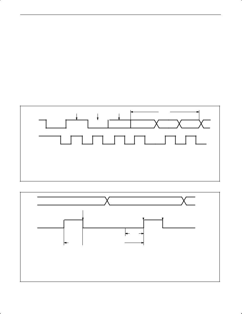
Philips Semiconductors Product data
80C51 8-bit Flash microcontroller family |
P89C660/P89C662/P89C664/ |
16KB/32KB/64KB ISP/IAP Flash with 512B/1KB/2KB/8KB RAM |
P89C668 |
|
|
Arbitration and Synchronization Logic
In the Master Transmitter mode, the arbitration logic checks that every transmitted logic 1 actually appears as a logic 1 on the I2C bus. If another device on the bus overrules a logic 1 and pulls the SDA line low, arbitration is lost, and SIO1 immediately changes from master transmitter to slave receiver. SIO1 will continue to output clock pulses (on SCL) until transmission of the current serial byte is complete.
Arbitration may also be lost in the Master Receiver mode. Loss of arbitration in this mode can only occur while SIO1 is returning a ªnot acknowledge: (logic 1) to the bus. Arbitration is lost when another device on the bus pulls this signal LOW. Since this can occur only at the end of a serial byte, SIO1 generates no further clock pulses. Figure 4 shows the arbitration procedure.
The synchronization logic will synchronize the serial clock generator with the clock pulses on the SCL line from another device. If two or more master devices generate clock pulses, the ªmarkº duration is determined by the device that generates the shortest ªmarks,º and the ªspaceº duration is determined by the device that generates the longest ªspaces.º Figure 5 shows the synchronization procedure.
A slave may stretch the space duration to slow down the bus master. The space duration may also be stretched for handshaking purposes. This can be done after each bit or after a complete byte transfer. SIO1 will stretch the SCL space duration after a byte has been transmitted or received and the acknowledge bit has been transferred. The serial interrupt flag (SI) is set, and the stretching continues until the serial interrupt flag is cleared.
|
|
|
|
|
(3) |
|
|
(1) |
(1) |
|
(2) |
|
|
SDA |
|
|
|
|
|
|
SCL |
1 |
2 |
3 |
4 |
8 |
9 |
|
|
|
|
|
|
|
|
|
|
|
|
|
ACK |
1.Another device transmits identical serial data.
2.Another device overrules a logic 1 (dotted line) transmitted by SIO1 (master) by pulling the SDA line low. Arbitration is lost, and SIO1 enters the slave receiver mode.
3.SIO1 is in the slave receiver mode but still generates clock pulses until the current byte has been transmitted. SIO1 will not generate clock pulses for the next byte. Data on SDA originates from the new master once it has won arbitration.
SU00967
Figure 4. Arbitration Procedure
SDA
(1) |
(3) |
(1) |
|
|
|
SCL
(2)
MARK 
 SPACE DURATION
DURATION
1.Another service pulls the SCL line low before the SIO1 ªmarkº duration is complete. The serial clock generator is immediately reset and commences with the ªspaceº duration by pulling SCL low.
2.Another device still pulls the SCL line low after SIO1 releases SCL. The serial clock generator is forced into the wait state until the SCL line is released.
3.The SCL line is released, and the serial clock generator commences with the mark duration.
SU00968
Figure 5. Serial Clock Synchronization
2002 Oct 28 |
15 |

Philips Semiconductors Product data
80C51 8-bit Flash microcontroller family |
P89C660/P89C662/P89C664/ |
16KB/32KB/64KB ISP/IAP Flash with 512B/1KB/2KB/8KB RAM |
P89C668 |
|
|
Serial Clock Generator
This programmable clock pulse generator provides the SCL clock pulses when SIO1 is in the Master Transmitter or Master Receiver mode. It is switched off when SIO1 is in a Slave mode. The programmable output clock frequencies are: fOSC/120, fOSC/9600
(12-clock mode) or fOSC/60, fOSC/4800 (6-clock mode) and the Timer 1 overflow rate divided by eight. The output clock pulses have
a 50% duty cycle unless the clock generator is synchronized with other SCL clock sources as described above.
Timing and Control
The timing and control logic generates the timing and control signals for serial byte handling. This logic block provides the shift pulses for
S1DAT, enables the comparator, generates and detects start and stop conditions, receives and transmits acknowledge bits, controls the master and Slave modes, contains interrupt request logic, and monitors the I2C bus status.
Control Register, S1CON
This 7-bit special function register is used by the microcontroller to control the following SIO1 functions: start and restart of a serial transfer, termination of a serial transfer, bit rate, address recognition, and acknowledgment.
Status Decoder and Status Register
The status decoder takes all of the internal status bits and compresses them into a 5-bit code. This code is unique for each I2C bus status. The 5-bit code may be used to generate vector addresses for fast processing of the various service routines. Each service routine processes a particular bus status. There are 26 possible bus states if all four modes of SIO1 are used. The 5-bit status code is latched into the five most significant bits of the status register when the serial interrupt flag is set (by hardware) and remains stable until the interrupt flag is cleared by software. The three least significant bits of the status register are always zero. If the status code is used as a vector to service routines, then the routines are displaced by eight address locations. Eight bytes of code is sufficient for most of the service routines.
this 8-bit, directly addressable SFR while it is not in the process of shifting a byte. This occurs when SIO1 is in a defined state and the serial interrupt flag is set. Data in S1DAT remains stable as long as SI is set. Data in S1DAT is always shifted from right to left: the first bit to be transmitted is the MSB (bit 7), and, after a byte has been received, the first bit of received data is located at the MSB of
S1DAT. While data is being shifted out, data on the bus is simultaneously being shifted in; S1DAT always contains the last data byte present on the bus. Thus, in the event of lost arbitration, the transition from master transmitter to slave receiver is made with the correct data in S1DAT.
7 |
6 |
5 |
4 |
3 |
2 |
1 |
0 |
|
|
|
|
|
|
|
|
|
|
S1DAT (DAH) |
SD7 |
SD6 |
SD5 |
SD4 |
SD3 |
SD2 |
SD1 |
SD0 |
|
|
|
|
|
|
|
|
|
shift direction
SD7 - SD0:
Eight bits to be transmitted or just received. A logic 1 in S1DAT corresponds to a high level on the I2C bus, and a logic 0 corresponds to a low level on the bus. Serial data shifts through
S1DAT from right to left. Figure 6 shows how data in S1DAT is serially transferred to and from the SDA line.
S1DAT and the ACK flag form a 9-bit shift register which shifts in or shifts out an 8-bit byte, followed by an acknowledge bit. The ACK flag is controlled by the SIO1 hardware and cannot be accessed by the CPU. Serial data is shifted through the ACK flag into S1DAT on the rising edges of serial clock pulses on the SCL line. When a byte has been shifted into S1DAT, the serial data is available in S1DAT, and the acknowledge bit is returned by the control logic during the ninth clock pulse. Serial data is shifted out from S1DAT via a buffer (BSD7) on the falling edges of clock pulses on the SCL line.
When the CPU writes to S1DAT, BSD7 is loaded with the content of S1DAT.7, which is the first bit to be transmitted to the SDA line (see
Figure 7). After nine serial clock pulses, the eight bits in S1DAT will have been transmitted to the SDA line, and the acknowledge bit will be present in ACK. Note that the eight transmitted bits are shifted back into S1DAT.
The Four SIO1 Special Function Registers
The microcontroller interfaces to SIO1 via four special function registers. These four SFRs (S1ADR, S1DAT, S1CON, and S1STA) are described individually in the following sections.
The Address Register, S1ADR
The CPU can read from and write to this 8-bit, directly addressable SFR. S1ADR is not affected by the SIO1 hardware. The contents of this register are irrelevant when SIO1 is in a Master mode. In the Slave modes, the seven most significant bits must be loaded with the microcontroller's own slave address, and, if the least significant bit is set, the general call address (00H) is recognized; otherwise it is ignored.
7 |
6 |
5 |
4 |
3 |
2 |
1 |
0 |
|||
|
|
|
|
|
|
|
|
|
|
|
S1ADR (DBH) |
X |
X |
X |
|
X |
X |
X |
X |
GC |
|
|
|
|
|
|
|
|
|
|
|
|
|
|
|
|
|
own slave address |
|
|
|
||
|
|
|
|
|
|
|
|
|||
|
|
|
|
|
|
|
|
|
|
|
The most significant bit corresponds to the first bit received from the I2C bus after a start condition. A logic 1 in S1ADR corresponds to a high level on the I2C bus, and a logic 0 corresponds to a low level on the bus.
The Data Register, S1DAT
S1DAT contains a byte of serial data to be transmitted or a byte which has just been received. The CPU can read from and write to
The Control Register, S1CON
The CPU can read from and write to this 8-bit, directly addressable SFR. Two bits are affected by the SIO1 hardware: the SI bit is set when a serial interrupt is requested, and the STO bit is cleared when a STOP condition is present on the I2C bus. The STO bit is also cleared when ENS1 = ª0º.
7 |
6 |
5 |
4 |
3 |
2 |
1 |
0 |
|
|
|
|
|
|
|
|
|
|
S1CON (D8H) |
CR2 |
ENS1 |
STA |
STO |
SI |
AA |
CR1 |
CR0 |
|
|
|
|
|
|
|
|
|
ENS1, the SIO1 Enable Bit: ENS1 = ª0º: When ENS1 is ª0º, the SDA and SCL outputs are in a high impedance state. SDA and SCL input signals are ignored, SIO1 is in the ªnot addressedº slave state, and the STO bit in S1CON is forced to ª0º. No other bits are affected. P1.6 and P1.7 may be used as open drain I/O ports.
ENS1 = ª1º: When ENS1 is ª1º, SIO1 is enabled. The P1.6 and P1.7 port latches must be set to logic 1.
ENS1 should not be used to temporarily release SIO1 from the I2C bus since, when ENS1 is reset, the I2C bus status is lost. The AA flag should be used instead (see description of the AA flag in the following text).
2002 Oct 28 |
16 |

Philips Semiconductors Product data
80C51 8-bit Flash microcontroller family |
P89C660/P89C662/P89C664/ |
16KB/32KB/64KB ISP/IAP Flash with 512B/1KB/2KB/8KB RAM |
P89C668 |
|
|
|
INTERNAL BUS |
|
SDA |
8 |
|
|
|
|
BSD7 |
S1DAT |
ACK |
SCL
SHIFT PULSES
SU00969
Figure 6. Serial Input/Output Configuration
SDA |
|
D7 |
D6 |
D5 |
D4 |
D3 |
D2 |
D1 |
D0 |
A |
|
|
|
|
|
|
|
|
|
|
|
|
|
SCL
SHIFT ACK & S1DAT
SHIFT IN
ACK |
|
|
|
(2) |
|
(2) |
|
|
(2) |
|
(2) |
|
(2) |
|
(2) |
|
(2) |
(2) |
|
|
A |
|
|||||||||||||
|
|
|
|
|
|
|
|
|
|
|
|
|
|
||||||||||||||||||||||
|
|
|
|
|
|
|
|
|
|
|
|
|
|
|
|
|
|
|
|
|
|
|
|
|
|
|
|
|
|
|
|
|
|
|
|
|
|
|
|
|
|
|
|
|
|
|
|
|
|
|
|
|
|
|
|
|
|
|
|
|
|
|
|
|
|
|
|
||||
S1DAT |
|
(1) |
|
(2) |
|
(2) |
|
|
(2) |
|
(2) |
|
(2) |
|
(2) |
|
(2) |
(2) |
|
(1) |
|
|
|||||||||||||
SHIFT BSD7 |
|
|
|
|
|
|
|
|
|
|
|
|
|
|
|
|
|
|
|
|
|
|
|
|
|
|
|
|
|
|
|
|
|
|
|
|
|
|
|
|
|
|
|
|
|
|
|
|
|
|
|
|
|
|
|
|
|
|
|
|
|
|
|
|
|
|
|
|
|
||
|
|
|
|
|
|
|
|
|
|
|
|
|
|
|
|
|
|
|
|
|
|
|
|
|
|
|
|
|
|
|
|
|
|
||
|
|
|
|
|
|
|
|
|
|
|
|
|
|
|
|
|
|
|
|
|
|
|
|
|
|
|
|
|
|
|
|
|
|
|
SHIFT OUT |
|
|
|
|
|
|
|
|
|
|
|
|
|
|
|
|
|
|
|
|
|
|
|
|
|
|
|
|
|
|
|
|
|
|
|
|
BSD7 |
|
|
D7 |
|
D6 |
D5 |
|
|
D4 |
|
|
|
D3 |
D2 |
|
D1 |
|
D0 |
(3) |
|
|
|
|||||||||||||
|
|
|
|
|
|
|
|
|
|
|
|
|
|
|
|||||||||||||||||||||
|
|
|
|
|
|
|
|
|
|
|
|
|
|
|
|
|
|
|
|
|
|
|
|
|
|
|
|
|
|
|
|
|
|
|
|
LOADED BY THE CPU
(1)Valid data in S1DAT
(2)Shifting data in S1DAT and ACK
(3)High level on SDA
SU00970
Figure 7. Shift-in and Shift-out Timing
In the following text, it is assumed that ENS1 = ª1º.
The ªSTARTº Flag, STA: STA = ª1º: When the STA bit is set to enter a Master mode, the SIO1 hardware checks the status of the I2C bus and generates a START condition if the bus is free. If the bus is not free, then SIO1 waits for a STOP condition (which will free the bus) and generates a START condition after a delay of half a clock period of the internal serial clock generator.
If STA is set while SIO1 is already in a Master mode and one or more bytes are transmitted or received, SIO1 transmits a repeated START condition. STA may be set at any time. STA may also be set when SIO1 is an addressed slave.
STA = ª0º: When the STA bit is reset, no START condition or repeated START condition will be generated.
The STOP Flag, STO: STO = ª1º: When the STO bit is set while SIO1 is in a Master mode, a STOP condition is transmitted to the I2C bus. When the STOP condition is detected on the bus, the SIO1 hardware clears the STO flag. In a Slave mode, the STO flag may be set to recover from an error condition. In this case, no STOP condition is transmitted to the I2C bus. However, the SIO1 hardware behaves as if a STOP condition has been received and switches to the defined ªnot addressedº Slave Receiver mode. The STO flag is automatically cleared by hardware.
2002 Oct 28 |
17 |

Philips Semiconductors Product data
80C51 8-bit Flash microcontroller family |
P89C660/P89C662/P89C664/ |
16KB/32KB/64KB ISP/IAP Flash with 512B/1KB/2KB/8KB RAM |
P89C668 |
|
|
If the STA and STO bits are both set, the a STOP condition is transmitted to the I2C bus if SIO1 is in a Master mode (in a Slave mode, SIO1 generates an internal STOP condition which is not transmitted). SIO1 then transmits a START condition.
STO = ª0º: When the STO bit is reset, no STOP condition will be generated.
The Serial Interrupt Flag, SI: SI = ª1º: When the SI flag is set, then, if the EA and ES1 (interrupt enable register) bits are also set, a
serial interrupt is requested. SI is set by hardware when one of 25 of the 26 possible SIO1 states is entered. The only state that does not cause SI to be set is state F8H, which indicates that no relevant state information is available.
While SI is set, the low period of the serial clock on the SCL line is stretched, and the serial transfer is suspended. A high level on the SCL line is unaffected by the serial interrupt flag. SI must be reset by software.
SI = ª0º: When the SI flag is reset, no serial interrupt is requested, and there is no stretching of the serial clock on the SCL line.
The Assert Acknowledge Flag, AA: AA = ª1º: If the AA flag is set, an acknowledge (low level to SDA) will be returned during the acknowledge clock pulse on the SCL line when:
±The ªown slave addressº has been received
±The general call address has been received while the general call bit (GC) in S1ADR is set
±A data byte has been received while SIO1 is in the Master Receiver mode
±A data byte has been received while SIO1 is in the addressed Slave Receiver mode
AA = ª0º: if the AA flag is reset, a not acknowledge (high level to SDA) will be returned during the acknowledge clock pulse on SCL when:
±A data has been received while SIO1 is in the Master Receiver mode
±A data byte has been received while SIO1 is in the addressed Slave Receiver mode
When SIO1 is in the addressed Slave Transmitter mode, state C8H will be entered after the last serial is transmitted (see Figure 11).
When SI is cleared, SIO1 leaves state C8H, enters the not addressed Slave Receiver mode, and the SDA line remains at a high level. In state C8H, the AA flag can be set again for future address recognition.
When SIO1 is in the not addressed Slave mode, its own slave address and the general call address are ignored. Consequently, no acknowledge is returned, and a serial interrupt is not requested.
Thus, SIO1 can be temporarily released from the I2C bus while the bus status is monitored. While SIO1 is released from the bus, START and STOP conditions are detected, and serial data is shifted in. Address recognition can be resumed at any time by setting the
AA flag. If the AA flag is set when the part's own Slave address or the general call address has been partly received, the address will be recognized at the end of the byte transmission.
The Clock Rate Bits CR0, CR1, and CR2: These three bits determine the serial clock frequency when SIO1 is in a Master mode. The various serial rates are shown in Table 3.
A 12.5 kHz bit rate may be used by devices that interface to the I2C bus via standard I/O port lines which are software driven and slow. 100 kHz is usually the maximum bit rate and can be derived from a
16 MHz, 12 MHz, or a 6 MHz oscillator. A variable bit rate (0.5 kHz to 62.5 kHz) may also be used if Timer 1 is not required for any other purpose while SIO1 is in a Master mode.
The frequencies shown in Table 3 are unimportant when SIO1 is in a Slave mode. In the Slave modes, SIO1 will automatically synchronize with any clock frequency up to 100 kHz.
The Status Register, S1STA
S1STA is an 8-bit read-only special function register. The three least significant bits are always zero. The five most significant bits contain the status code. There are 26 possible status codes. When S1STA contains F8H, no relevant state information is available and no serial interrupt is requested. All other S1STA values correspond to defined SIO1 states. When each of these states is entered, a serial interrupt is requested (SI = ª1º). A valid status code is present in S1STA one machine cycle after SI is set by hardware and is still present one machine cycle after SI has been reset by software.
2002 Oct 28 |
18 |

Philips Semiconductors Product data
80C51 8-bit Flash microcontroller family |
|
P89C660/P89C662/P89C664/ |
||||||||
16KB/32KB/64KB ISP/IAP Flash with 512B/1KB/2KB/8KB RAM |
|
P89C668 |
||||||||
|
|
|
|
|
|
|
|
|
|
|
Table 3. |
Serial Clock Rates |
|
|
|
|
|
||||
|
|
|
|
|
|
|
|
|
|
|
6-clock mode |
|
|
|
|
|
|
|
|||
|
|
|
|
|
|
|
|
|
|
|
|
|
|
|
|
|
BIT FREQUENCY (kHz) AT fOSC |
|
|
||
CR2 |
|
CR1 |
|
CR0 |
3 MHz |
6 MHz |
8 MHz |
12 MHz2 |
15 MHz2 |
fOSC DIVIDED BY |
0 |
|
0 |
|
0 |
23 |
47 |
62.5 |
94 |
1171 |
128 |
0 |
|
0 |
|
1 |
27 |
54 |
71 |
1071 |
1341 |
112 |
0 |
|
1 |
|
0 |
31 |
63 |
83.3 |
1251 |
1561 |
96 |
0 |
|
1 |
|
1 |
37 |
75 |
100 |
1501 |
1881 |
80 |
1 |
|
0 |
|
0 |
6.25 |
12.5 |
17 |
25 |
31 |
480 |
1 |
|
0 |
|
1 |
50 |
100 |
1331 |
2001 |
2501 |
60 |
1 |
|
1 |
|
0 |
100 |
200 |
2671 |
4001 |
5001 |
30 |
1 |
|
1 |
|
1 |
0.24 < 62.5 |
0.49 < 62.5 |
0.65 < 55.6 |
0.98 < 50.0 |
1.22 < 52.1 |
48 × (256 ± (reload value Timer 1)) |
|
|
|
|
|
0 < 255 |
0 < 254 |
0 < 253 |
0 < 251 |
0 < 250 |
Reload value Timer 1 in Mode 2. |
|
|
|
|
|
|
|
||||
12-clock mode |
|
|
|
|
|
|
||||
|
|
|
|
|
|
|
|
|
||
|
|
|
|
|
|
BIT FREQUENCY (kHz) AT fOSC |
|
|
||
CR2 |
|
CR1 |
|
CR0 |
6 MHz |
12 MHz |
16 MHz |
24 MHz3 |
30 MHz3 |
fOSC DIVIDED BY |
0 |
|
0 |
|
0 |
23 |
47 |
62.5 |
94 |
1171 |
256 |
0 |
|
0 |
|
1 |
27 |
54 |
71 |
1071 |
1341 |
224 |
0 |
|
1 |
|
0 |
31 |
63 |
83.3 |
1251 |
1561 |
192 |
0 |
|
1 |
|
1 |
37 |
75 |
100 |
1501 |
1881 |
160 |
1 |
|
0 |
|
0 |
6.25 |
12.5 |
17 |
25 |
31 |
960 |
1 |
|
0 |
|
1 |
50 |
100 |
1331 |
2001 |
2501 |
120 |
1 |
|
1 |
|
0 |
100 |
200 |
2671 |
4001 |
5001 |
60 |
1 |
|
1 |
|
1 |
0.24 < 62.5 |
0.49 < 62.5 |
0.65 < 55.6 |
0.98 < 50.0 |
1.22 < 52.1 |
96 × (256 ± (reload value Timer 1)) |
|
|
|
|
|
0 < 255 |
0 < 254 |
0 < 253 |
0 < 251 |
0 < 250 |
Reload value Timer 1 in Mode 2. |
NOTES:
1.These frequencies exceed the upper limit of 100 kHz of the I2C-bus specification and cannot be used in an I2C-bus application.
2.At fOSC = 12 MHz/15 MHz the maximum I2C bus rate of 100 kHz cannot be realized due to the fixed divider rates.
3.At fOSC = 24 MHz/30 MHz the maximum I2C bus rate of 100 kHz cannot be realized due to the fixed divider rates.
2002 Oct 28 |
19 |

Philips Semiconductors Product data
80C51 8-bit Flash microcontroller family |
P89C660/P89C662/P89C664/ |
16KB/32KB/64KB ISP/IAP Flash with 512B/1KB/2KB/8KB RAM |
P89C668 |
|
|
More Information on SIO1 Operating Modes
The four operating modes are:
±Master Transmitter
±Master Receiver
±Slave Receiver
±Slave Transmitter
Data transfers in each mode of operation are shown in Figures 8-11.
These figures contain the following abbreviations:
Abbreviation |
Explanation |
|
S |
Start condition |
|
SLA |
7-bit slave address |
|
R |
Read bit (high level at SDA) |
|
W |
Write bit (low level at SDA) |
|
A |
Acknowledge bit (low level at SDA) |
|
A |
|
Not acknowledge bit (high level at SDA) |
Data |
8-bit data byte |
|
P |
Stop condition |
|
In Figures 8-11, circles are used to indicate when the serial interrupt flag is set. The numbers in the circles show the status code held in the S1STA register. At these points, a service routine must be executed to continue or complete the serial transfer. These service routines are not critical since the serial transfer is suspended until the serial interrupt flag is cleared by software.
When a serial interrupt routine is entered, the status code in S1STA is used to branch to the appropriate service routine. For each status code, the required software action and details of the following serial transfer are given in Tables 4-8.
may switch to the Master Receiver mode by loading S1DAT with SLA+R).
Master Receiver mode
In the Master Receiver mode, a number of data bytes are received from a slave transmitter (see Figure 9). The transfer is initialized as in the Master Transmitter mode. When the start condition has been transmitted, the interrupt service routine must load S1DAT with the 7-bit slave address and the data direction bit (SLA+R). The SI bit in S1CON must then be cleared before the serial transfer can continue.
When the slave address and the data direction bit have been transmitted and an acknowledgment bit has been received, the serial interrupt flag (SI) is set again, and a number of status codes in S1STA are possible. These are 40H, 48H, or 38H for the Master mode and also 68H, 78H, or B0H if the Slave mode was enabled (AA = logic 1). The appropriate action to be taken for each of these status codes is detailed in Table 5. ENS1, CR1, and CR0 are not affected by the serial transfer and are not referred to in Table 5. After a repeated start condition (state 10H), SIO1 may switch to the Master Transmitter mode by loading S1DAT with SLA+W.
Slave Receiver mode
In the Slave Receiver mode, a number of data bytes are received from a master transmitter (see Figure 10). To initiate the Slave Receiver mode, S1ADR and S1CON must be loaded as follows:
7 |
6 |
|
5 |
4 |
3 |
|
2 |
1 |
0 |
||
|
|
|
|
|
|
|
|
|
|
|
|
S1ADR (DBH) |
X |
X |
|
X |
|
X |
X |
|
X |
X |
GC |
|
|
|
|
|
|
|
|
|
|
|
|
|
|
|
|
|
own slave address |
|
|
|
|||
|
|
|
|
|
|
|
|
||||
|
|
|
|
|
|
|
|
|
|
|
|
Master Transmitter mode
In the Master Transmitter mode, a number of data bytes are transmitted to a slave receiver (see Figure 8). Before the Master
Transmitter mode can be entered, S1CON must be initialized as follows:
7 |
6 |
5 |
4 |
3 |
2 |
1 |
0 |
|
||
|
|
|
|
|
|
|
|
|
|
|
S1CON (D8H) |
CR2 |
ENS1 |
STA |
STO |
SI |
AA |
CR1 |
CR0 |
||
|
|
|
|
|
|
|
|
|
|
|
|
bit |
1 |
0 |
0 |
0 |
X |
|
bit rate |
|
|
|
rate |
|
|
|
|
|
|
|
|
|
CR0, CR1, and CR2 define the serial bit rate. ENS1 must be set to logic 1 to enable SIO1. If the AA bit is reset, SIO1 will not acknowledge its own slave address or the general call address in the event of another device becoming master of the bus. In other words, if AA is reset, SIO0 cannot enter a Slave mode. STA, STO, and SI must be reset.
The Master Transmitter mode may now be entered by setting the STA bit using the SETB instruction. The SIO1 logic will now test the I2C bus and generate a start condition as soon as the bus becomes free. When a START condition is transmitted, the serial interrupt flag (SI) is set, and the status code in the status register (S1STA) will be 08H. This status code must be used to vector to an interrupt service routine that loads S1DAT with the slave address and the data direction bit (SLA+W). The SI bit in S1CON must then be reset before the serial transfer can continue.
When the slave address and the direction bit have been transmitted and an acknowledgment bit has been received, the serial interrupt flag (SI) is set again, and a number of status codes in S1STA are possible. There are 18H, 20H, or 38H for the Master mode and also
68H, 78H, or B0H if the Slave mode was enabled (AA = logic 1). The appropriate action to be taken for each of these status codes is detailed in Table 4. After a repeated start condition (state 10H). SIO1
The upper 7 bits are the address to which SIO1 will respond when addressed by a master. If the LSB (GC) is set, SIO1 will respond to the general call address (00H); otherwise it ignores the general call address.
7 |
6 |
5 |
4 |
3 |
2 |
1 |
0 |
|
|
|
|
|
|
|
|
|
|
S1CON (D8H) |
CR2 |
ENS1 |
STA |
STO |
SI |
AA |
CR1 |
CR0 |
|
|
|
|
|
|
|
|
|
|
X |
1 |
0 |
0 |
0 |
1 |
X |
X |
CR0, CR1, and CR2 do not affect SIO1 in the Slave mode. ENS1 must be set to logic 1 to enable SIO1. The AA bit must be set to enable SIO1 to acknowledge its own slave address or the general call address. STA, STO, and SI must be reset.
When S1ADR and S1CON have been initialized, SIO1 waits until it is addressed by its own slave address followed by the data direction bit which must be ª0º (W) for SIO1 to operate in the Slave Receiver mode. After its own slave address and the W bit have been received, the serial interrupt flag (I) is set and a valid status code can be read from S1STA. This status code is used to vector to an interrupt service routine, and the appropriate action to be taken for each of these status codes is detailed in Table 6. The Slave Receiver mode may also be entered if arbitration is lost while SIO1 is in the Master mode (see status 68H and 78H).
If the AA bit is reset during a transfer, SIO1 will return a not acknowledge (logic 1) to SDA after the next received data byte. While AA is reset, SIO1 does not respond to its own slave address or a general call address. However, the I2C bus is still monitored and address recognition may be resumed at any time by setting AA. This means that the AA bit may be used to temporarily isolate SIO1 from the I2C bus.
2002 Oct 28 |
20 |
Philips Semiconductors Product data
80C51 8-bit Flash microcontroller family |
P89C660/P89C662/P89C664/ |
16KB/32KB/64KB ISP/IAP Flash with 512B/1KB/2KB/8KB RAM |
P89C668 |
|
|
|
|
|
|
MT |
|
|
|
|
SUCCESSFUL TRANSMISSION |
S |
SLA |
W |
A |
DATA |
A |
P |
|
TO A SLAVE RECEIVER |
|
|||||||
|
|
|
|
|
|
|
|
|
|
08H |
|
|
18H |
|
28H |
|
|
NEXT TRANSFER STARTED WITH A REPEATED START CONDITION |
|
|
S |
SLA |
W |
|||
|
|
|
|
|
|
|||
|
|
|
|
|
|
10H |
|
|
NOT ACKNOWLEDGE RECEIVED AFTER THE SLAVE ADDRESS |
|
A |
P |
|
|
R |
||
|
|
|
|
|
|
|||
|
|
|
|
20H |
|
|
|
|
|
|
|
|
|
|
|
TO MST/REC MODE |
NOT ACKNOWLEDGE RECEIVED AFTER A DATA BYTE |
|
|
|
|
ENTRY = MR |
||
|
|
|
A |
P |
|||
|
|
|
|
|
|
||
|
|
|
|
|
|
30H |
|
ARBITRATION LOST IN SLAVE ADDRESS OR DATA BYTE |
A or A |
OTHER MST |
A or A |
OTHER MST |
|||
|
|
|
CONTINUES |
CONTINUES |
|||
|
|
|
|
|
|||
|
|
|
38H |
|
|
38H |
|
ARBITRATION LOST AND ADDRESSED AS SLAVE |
A |
OTHER MST |
|
|
|||
|
|
|
CONTINUES |
|
|
||
|
|
|
|
|
|
||
|
|
|
68H |
78H |
80H |
TO CORRESPONDING |
|
|
|
|
STATES IN SLAVE MODE |
||||
|
|
|
|
|
|
||
|
|
FROM MASTER TO SLAVE |
|
|
|
|
|
|
|
FROM SLAVE TO MASTER |
|
|
|
|
|
Data |
A |
ANY NUMBER OF DATA BYTES AND THEIR ASSOCIATED ACKNOWLEDGE BITS |
|
|
|||
n |
THIS NUMBER (CONTAINED IN S1STA) CORRESPONDS TO A DEFINED STATE OF THE I2C BUS. SEE TABLE 4. |
||||||
|
|
|
|
|
|
|
|
|
|
|
|
|
|
|
SU00971 |
Figure 8. Format and States in the Master Transmitter mode
2002 Oct 28 |
21 |
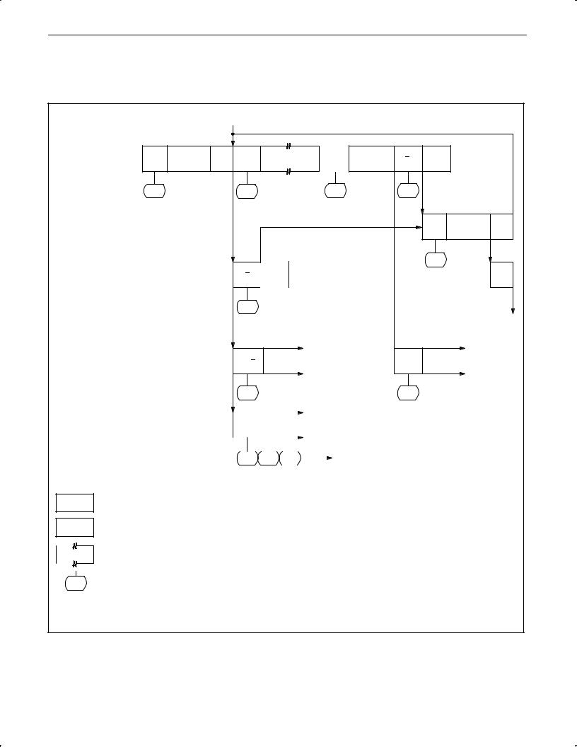
Philips Semiconductors Product data
80C51 8-bit Flash microcontroller family |
P89C660/P89C662/P89C664/ |
16KB/32KB/64KB ISP/IAP Flash with 512B/1KB/2KB/8KB RAM |
P89C668 |
|
|
|
|
|
|
MR |
|
|
|
|
|
|
|
SUCCESSFUL RECEPTION |
S |
SLA |
R |
A |
DATA |
A |
DATA |
A |
P |
|
|
FROM A SLAVE TRANSMITTER |
|
|
|||||||||
|
|
|
|
|
|
|
|
|
|
|
|
|
08H |
|
|
40H |
|
50H |
|
58H |
|
|
|
NEXT TRANSFER STARTED WITH A |
|
|
|
|
|
|
|
S |
SLA |
R |
|
REPEATED START CONDITION |
|
|
|
|
|
|
|
|
|||
|
|
|
|
|
|
|
|
|
|
|
|
|
|
|
|
|
|
|
|
|
10H |
|
|
NOT ACKNOWLEDGE RECEIVED |
|
|
|
A |
P |
|
|
|
|
|
W |
AFTER THE SLAVE ADDRESS |
|
|
|
|
|
|
|
|
|||
|
|
|
|
|
|
|
|
|
|
|
|
|
|
|
|
48H |
|
|
|
|
|
|
|
|
|
|
|
|
|
|
|
|
|
TO MST/TRX MODE |
|
|
|
|
|
|
|
|
|
|
|
ENTRY = MT |
|
ARBITRATION LOST IN SLAVE ADDRESS |
|
|
A or A |
OTHER MST |
|
|
A |
OTHER MST |
|
||
OR ACKNOWLEDGE BIT |
|
|
|
CONTINUES |
|
|
CONTINUES |
|
|||
|
|
|
|
|
|
|
|
||||
|
|
|
|
38H |
|
|
|
38H |
|
|
|
|
|
|
|
|
|
|
|
|
|
|
ARBITRATION LOST AND ADDRESSED AS SLAVE |
|
A |
OTHER MST |
|
||||||
|
|
CONTINUES |
|
|||||||
|
|
|
|
|
|
|||||
|
|
|
|
|
|
|
|
|
|
TO CORRESPONDING |
|
|
|
|
|
|
|
|
|
|
|
|
|
68H |
78H |
80H |
|
|||||
|
|
|
STATES IN SLAVE MODE |
|||||||
|
|
|
|
|
|
|
|
|
|
|
FROM MASTER TO SLAVE
FROM SLAVE TO MASTER
|
|
|
|
|
ANY NUMBER OF DATA BYTES AND THEIR ASSOCIATED ACKNOWLEDGE BITS |
DATA |
|
A |
|
||
|
|
|
|||
|
|
|
|
|
|
n |
THIS NUMBER (CONTAINED IN S1STA) CORRESPONDS TO A DEFINED STATE OF THE I2C BUS. SEE TABLE 5. |
|
SU00972
Figure 9. Format and States in the Master Receiver Mode
2002 Oct 28 |
22 |
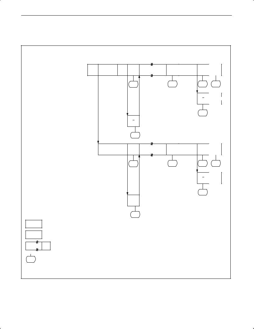
Philips Semiconductors Product data
80C51 8-bit Flash microcontroller family |
P89C660/P89C662/P89C664/ |
16KB/32KB/64KB ISP/IAP Flash with 512B/1KB/2KB/8KB RAM |
P89C668 |
|
|
RECEPTION OF THE OWN SLAVE ADDRESS |
|
|
|
|
|
|
|
|
|
AND ONE OR MORE DATA BYTES |
S |
SLA |
W |
A |
DATA |
A |
DATASLA |
A |
P or S |
ALL ARE ACKNOWLEDGED. |
|
|
|
|
|
|
|
|
|
|
|
|
|
60H |
|
80H |
|
80H |
A0H |
LAST DATA BYTE RECEIVED IS |
|
|
|
|
|
|
|
A |
P or S |
NOT ACKNOWLEDGED |
|
|
|
|
|
|
|
||
|
|
|
|
|
|
|
|
|
|
|
|
|
|
|
|
|
|
88H |
|
ARBITRATION LOST AS MST AND |
|
|
|
A |
|
|
|
|
|
ADDRESSED AS SLAVE |
|
|
|
|
|
|
|
|
|
|
|
|
|
|
|
|
|
|
|
|
|
|
|
68H |
|
|
|
|
|
RECEPTION OF THE GENERAL CALL ADDRESS |
|
GENERAL |
|
|
|
|
DATA |
|
|
AND ONE OR MORE DATA BYTES |
|
|
A |
DATA |
A |
A |
P or S |
||
|
CALL |
|
|||||||
|
|
|
|
|
|
|
|
|
|
|
|
|
|
70H |
|
90H |
|
90H |
A0H |
LAST DATA BYTE IS NOT ACKNOWLEDGED |
|
|
|
|
|
|
|
A |
P or S |
|
|
|
|
|
|
|
|
||
|
|
|
|
|
|
|
|
98H |
|
ARBITRATION LOST AS MST AND ADDRESSED AS SLAVE BY GENERAL CALL |
|
A |
|
|
|
|
|
||
|
|
|
|
|
|
|
|
|
|
78H
FROM MASTER TO SLAVE
FROM SLAVE TO MASTER
Data |
A |
ANY NUMBER OF DATA BYTES AND THEIR ASSOCIATED ACKNOWLEDGE BITS |
n |
THIS NUMBER (CONTAINED IN S1STA) CORRESPONDS TO A DEFINED STATE OF THE I2C BUS. SEE TABLE 6. |
|
SU00973
Figure 10. Format and States in the Slave Receiver mode
2002 Oct 28 |
23 |
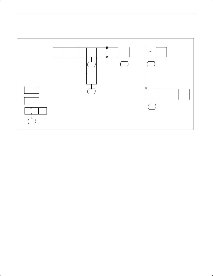
Philips Semiconductors Product data
80C51 8-bit Flash microcontroller family |
P89C660/P89C662/P89C664/ |
16KB/32KB/64KB ISP/IAP Flash with 512B/1KB/2KB/8KB RAM |
P89C668 |
|
|
RECEPTION OF THE |
|
|
|
|
|
|
|
|
|
|
|
OWN SLAVE ADDRESS |
S |
SLA |
R |
A |
DATA |
A |
DATA |
A |
P or S |
|
|
AND TRANSMISSION |
|
||||||||||
|
|
|
|
|
|
|
|
|
|
||
OF ONE OR MORE |
|
|
|
|
|
|
|
|
|
|
|
DATA BYTES |
|
|
|
|
|
|
|
|
|
|
|
|
|
|
|
|
A8H |
|
B8H |
|
C0H |
|
|
|
|
|
|
|
A |
ARBITRATION LOST AS MST |
|
|
|
|
|
|
|
|
|
|
AND ADDRESSED AS SLAVE |
|
|
|
|
||
|
FROM MASTER TO SLAVE |
|
B0H |
LAST DATA BYTE TRANSMITTED. |
|
|
|
||||
|
|
|
|
|
|
|
|
||||
|
|
|
|
|
|
|
|
P or S |
|||
|
|
|
|
|
|
SWITCHED TO NOT ADDRESSED |
A |
All ª1ºs |
|||
|
|
|
|
|
|
SLAVE (AA BIT IN S1CON = ª0º |
|
|
|
||
|
FROM SLAVE TO MASTER |
|
|
|
|
|
|
|
|
||
|
|
|
|
|
|
|
|
|
C8H |
|
|
DATA |
A |
ANY NUMBER OF DATA BYTES AND THEIR ASSOCIATED ACKNOWLEDGE BITS |
|
|
|
|
|||||
n THIS NUMBER (CONTAINED IN S1STA) CORRESPONDS TO A DEFINED STATE OF THE I2C BUS. SEE TABLE 7.
SU00974
Figure 11. Format and States of the Slave Transmitter mode
2002 Oct 28 |
24 |

Philips Semiconductors Product data
80C51 8-bit Flash microcontroller family |
|
P89C660/P89C662/P89C664/ |
|||||||
16KB/32KB/64KB ISP/IAP Flash with 512B/1KB/2KB/8KB RAM |
|
P89C668 |
|||||||
|
|
|
|
|
|
|
|
|
|
Table 4. |
Master Transmitter mode |
|
|
|
|
|
|||
|
|
|
|
|
|
|
|
|
|
STATUS |
STATUS OF THE |
APPLICATION SOFTWARE RESPONSE |
|
||||||
|
|
|
|
|
|
||||
CODE |
I2C BUS AND |
TO/FROM S1DAT |
|
TO S1CON |
|
NEXT ACTION TAKEN BY SIO1 HARDWARE |
|||
(S1STA) |
SIO1 HARDWARE |
|
|
|
|
|
|||
STA |
STO |
SI |
AA |
|
|||||
|
|
||||||||
|
|
|
|
|
|
||||
|
|
|
|
|
|
|
|
|
|
08H |
A START condition has |
Load SLA+W |
X |
0 |
0 |
X |
SLA+W will be transmitted; |
||
|
been transmitted |
|
|
|
|
|
ACK bit will be received |
||
|
|
|
|
|
|
|
|
|
|
10H |
A repeated START |
Load SLA+W or |
X |
0 |
0 |
X |
As above |
||
|
condition has been |
Load SLA+R |
X |
0 |
0 |
X |
SLA+W will be transmitted; |
||
|
transmitted |
|
|
|
|
|
SIO1 will be switched to MST/REC mode |
||
|
|
|
|
|
|
|
|
|
|
18H |
SLA+W has been |
Load data byte or |
0 |
0 |
0 |
X |
Data byte will be transmitted; |
||
|
transmitted; ACK has |
|
|
|
|
|
ACK bit will be received |
||
|
been received |
no S1DAT action or |
1 |
0 |
0 |
X |
Repeated START will be transmitted; |
||
|
|
|
|
no S1DAT action or |
0 |
1 |
0 |
X |
STOP condition will be transmitted; |
|
|
|
|
|
|
|
|
|
STO flag will be reset |
|
|
|
|
no S1DAT action |
1 |
1 |
0 |
X |
STOP condition followed by a |
|
|
|
|
|
|
|
|
|
START condition will be transmitted; |
|
|
|
|
|
|
|
|
|
STO flag will be reset |
20H |
SLA+W has been |
Load data byte or |
0 |
0 |
0 |
X |
Data byte will be transmitted; |
||
|
transmitted; NOT ACK |
|
|
|
|
|
ACK bit will be received |
||
|
has been received |
no S1DAT action or |
1 |
0 |
0 |
X |
Repeated START will be transmitted; |
||
|
|
|
|
no S1DAT action or |
0 |
1 |
0 |
X |
STOP condition will be transmitted; |
|
|
|
|
|
|
|
|
|
STO flag will be reset |
|
|
|
|
no S1DAT action |
1 |
1 |
0 |
X |
STOP condition followed by a |
|
|
|
|
|
|
|
|
|
START condition will be transmitted; |
|
|
|
|
|
|
|
|
|
STO flag will be reset |
|
|
|
|
|
|
|
|
|
|
28H |
Data byte in S1DAT has |
Load data byte or |
0 |
0 |
0 |
X |
Data byte will be transmitted; |
||
|
been transmitted; ACK |
|
|
|
|
|
ACK bit will be received |
||
|
has been received |
no S1DAT action or |
1 |
0 |
0 |
X |
Repeated START will be transmitted; |
||
|
|
|
|
no S1DAT action or |
0 |
1 |
0 |
X |
STOP condition will be transmitted; |
|
|
|
|
|
|
|
|
|
STO flag will be reset |
|
|
|
|
no S1DAT action |
1 |
1 |
0 |
X |
STOP condition followed by a |
|
|
|
|
|
|
|
|
|
START condition will be transmitted; |
|
|
|
|
|
|
|
|
|
STO flag will be reset |
|
|
|
|
|
|
|
|
|
|
30H |
Data byte in S1DAT has |
Load data byte or |
0 |
0 |
0 |
X |
Data byte will be transmitted; |
||
|
been transmitted; NOT |
|
|
|
|
|
ACK bit will be received |
||
|
ACK has been received |
no S1DAT action or |
1 |
0 |
0 |
X |
Repeated START will be transmitted; |
||
|
|
|
|
no S1DAT action or |
0 |
1 |
0 |
X |
STOP condition will be transmitted; |
|
|
|
|
|
|
|
|
|
STO flag will be reset |
|
|
|
|
no S1DAT action |
1 |
1 |
0 |
X |
STOP condition followed by a |
|
|
|
|
|
|
|
|
|
START condition will be transmitted; |
|
|
|
|
|
|
|
|
|
STO flag will be reset |
38H |
Arbitration lost in |
No S1DAT action or |
0 |
0 |
0 |
X |
I2C bus will be released; |
||
|
SLA+R/W |
|
or |
|
|
|
|
|
not addressed slave will be entered |
|
Data bytes |
No S1DAT action |
1 |
0 |
0 |
X |
A START condition will be transmitted when the |
||
|
|
|
|
|
|
|
|
|
bus becomes free |
2002 Oct 28 |
25 |

Philips Semiconductors Product data
80C51 8-bit Flash microcontroller family |
|
|
P89C660/P89C662/P89C664/ |
|||||
16KB/32KB/64KB ISP/IAP Flash with 512B/1KB/2KB/8KB RAM |
|
P89C668 |
||||||
|
|
|
|
|
|
|
|
|
Table 5. |
Master Receiver Mode |
|
|
|
|
|
|
|
|
|
|
|
|
|
|
|
|
STATUS |
STATUS OF THE I2C |
APPLICATION SOFTWARE RESPONSE |
|
|
||||
|
|
|
|
|
|
|
||
CODE |
BUS AND |
TO/FROM S1DAT |
|
TO S1CON |
|
NEXT ACTION TAKEN BY SIO1 HARDWARE |
||
(S1STA) |
SIO1 HARDWARE |
|
|
|
|
|
|
|
STA |
STO |
SI |
|
AA |
|
|||
|
|
|
||||||
|
|
|
|
|
||||
|
|
|
|
|
|
|
|
|
08H |
A START condition has |
Load SLA+R |
X |
0 |
0 |
|
X |
SLA+R will be transmitted; |
|
been transmitted |
|
|
|
|
|
|
ACK bit will be received |
|
|
|
|
|
|
|
|
|
10H |
A repeated START |
Load SLA+R or |
X |
0 |
0 |
|
X |
As above |
|
condition has been |
Load SLA+W |
X |
0 |
0 |
|
X |
SLA+W will be transmitted; |
|
transmitted |
|
|
|
|
|
|
SIO1 will be switched to MST/TRX mode |
|
|
|
|
|
|
|
|
|
38H |
Arbitration lost in |
No S1DAT action or |
0 |
0 |
0 |
|
X |
I2C bus will be released; |
|
NOT ACK bit |
|
|
|
|
|
|
SIO1 will enter a Slave mode |
|
|
No S1DAT action |
1 |
0 |
0 |
|
X |
A START condition will be transmitted when the |
|
|
|
|
|
|
|
|
bus becomes free |
|
|
|
|
|
|
|
|
|
40H |
SLA+R has been |
No S1DAT action or |
0 |
0 |
0 |
|
0 |
Data byte will be received; |
|
transmitted; ACK has |
|
|
|
|
|
|
NOT ACK bit will be returned |
|
been received |
no S1DAT action |
0 |
0 |
0 |
|
1 |
Data byte will be received; |
|
|
|
|
|
|
|
|
ACK bit will be returned |
|
|
|
|
|
|
|
|
|
48H |
SLA+R has been |
No S1DAT action or |
1 |
0 |
0 |
|
X |
Repeated START condition will be transmitted |
|
transmitted; NOT ACK |
no S1DAT action or |
0 |
1 |
0 |
|
X |
STOP condition will be transmitted; |
|
has been received |
|
|
|
|
|
|
STO flag will be reset |
|
|
no S1DAT action |
1 |
1 |
0 |
|
X |
STOP condition followed by a |
|
|
|
|
|
|
|
|
START condition will be transmitted; |
|
|
|
|
|
|
|
|
STO flag will be reset |
|
|
|
|
|
|
|
|
|
50H |
Data byte has been |
Read data byte or |
0 |
0 |
0 |
|
0 |
Data byte will be received; |
|
received; ACK has been |
|
|
|
|
|
|
NOT ACK bit will be returned |
|
returned |
read data byte |
0 |
0 |
0 |
|
1 |
Data byte will be received; |
|
|
|
|
|
|
|
|
ACK bit will be returned |
|
|
|
|
|
|
|
|
|
58H |
Data byte has been |
Read data byte or |
1 |
0 |
0 |
|
X |
Repeated START condition will be transmitted |
|
received; NOT ACK has |
read data byte or |
0 |
1 |
0 |
|
X |
STOP condition will be transmitted; |
|
been returned |
|
|
|
|
|
|
STO flag will be reset |
|
|
read data byte |
1 |
1 |
0 |
|
X |
STOP condition followed by a |
|
|
|
|
|
|
|
|
START condition will be transmitted; |
|
|
|
|
|
|
|
|
STO flag will be reset |
2002 Oct 28 |
26 |

Philips Semiconductors Product data
80C51 8-bit Flash microcontroller family |
|
|
P89C660/P89C662/P89C664/ |
||||||
16KB/32KB/64KB ISP/IAP Flash with 512B/1KB/2KB/8KB RAM |
P89C668 |
||||||||
|
|
|
|
|
|
|
|
|
|
Table 6. |
Slave Receiver mode |
|
|
|
|
|
|||
|
|
|
|
|
|
|
|
|
|
STATUS |
STATUS OF THE |
APPLICATION SOFTWARE RESPONSE |
|
||||||
|
|
|
|
|
|
||||
CODE |
I2C BUS AND |
TO/FROM S1DAT |
|
TO S1CON |
|
NEXT ACTION TAKEN BY SIO1 HARDWARE |
|||
(S1STA) |
SIO1 HARDWARE |
|
|
|
|
|
|||
STA |
STO |
SI |
AA |
|
|||||
|
|
||||||||
|
|
|
|
|
|
||||
|
|
|
|
|
|
|
|
|
|
60H |
Own SLA+W has |
No S1DAT action or |
X |
0 |
0 |
0 |
Data byte will be received and NOT ACK will be |
||
|
been received; ACK |
|
|
|
|
|
returned |
||
|
has been returned |
no S1DAT action |
X |
0 |
0 |
1 |
Data byte will be received and ACK will be returned |
||
|
|
|
|
|
|
|
|
||
68H |
Arbitration lost in |
No S1DAT action or |
X |
0 |
0 |
0 |
Data byte will be received and NOT ACK will be |
||
|
SLA+R/W |
|
as master; |
|
|
|
|
|
returned |
|
Own SLA+W has |
|
|
|
|
|
|
||
|
been received, ACK |
no S1DAT action |
X |
0 |
0 |
1 |
Data byte will be received and ACK will be returned |
||
|
returned |
|
|
|
|
|
|
||
|
|
|
|
|
|
|
|
||
70H |
General call address |
No S1DAT action or |
X |
0 |
0 |
0 |
Data byte will be received and NOT ACK will be |
||
|
(00H) has been |
|
|
|
|
|
returned |
||
|
received; ACK has |
no S1DAT action |
X |
0 |
0 |
1 |
Data byte will be received and ACK will be returned |
||
|
been returned |
||||||||
|
|
|
|
|
|
|
|||
|
|
|
|
|
|
|
|
||
78H |
Arbitration lost in |
No S1DAT action or |
X |
0 |
0 |
0 |
Data byte will be received and NOT ACK will be |
||
|
SLA+R/W |
|
as master; |
|
|
|
|
|
returned |
|
General call address |
|
|
|
|
|
|
||
|
has been received, |
no S1DAT action |
X |
0 |
0 |
1 |
Data byte will be received and ACK will be returned |
||
|
ACK has been |
||||||||
|
|
|
|
|
|
|
|||
|
returned |
|
|
|
|
|
|
||
|
|
|
|
|
|
|
|
||
80H |
Previously addressed |
Read data byte or |
X |
0 |
0 |
0 |
Data byte will be received and NOT ACK will be |
||
|
with own SLV |
|
|
|
|
|
returned |
||
|
address; DATA has |
|
|
|
|
|
|
||
|
been received; ACK |
read data byte |
X |
0 |
0 |
1 |
Data byte will be received and ACK will be returned |
||
|
has been returned |
|
|
|
|
|
|
||
|
|
|
|
|
|
|
|
||
88H |
Previously addressed |
Read data byte or |
0 |
0 |
0 |
0 |
Switched to not addressed SLV mode; no recognition |
||
|
with own SLA; DATA |
|
|
|
|
|
of own SLA or General call address |
||
|
byte has been |
read data byte or |
0 |
0 |
0 |
1 |
Switched to not addressed SLV mode; Own SLA will |
||
|
received; NOT ACK |
|
|
|
|
|
be recognized; General call address will be |
||
|
has been returned |
|
|
|
|
|
recognized if S1ADR.0 = logic 1 |
||
|
|
|
|
read data byte or |
1 |
0 |
0 |
0 |
Switched to not addressed SLV mode; no recognition |
|
|
|
|
|
|
|
|
|
of own SLA or General call address. A START |
|
|
|
|
|
|
|
|
|
condition will be transmitted when the bus becomes |
|
|
|
|
|
|
|
|
|
free |
|
|
|
|
read data byte |
1 |
0 |
0 |
1 |
Switched to not addressed SLV mode; Own SLA will |
|
|
|
|
|
|
|
|
|
be recognized; General call address will be |
|
|
|
|
|
|
|
|
|
recognized if S1ADR.0 = logic 1. A START condition |
|
|
|
|
|
|
|
|
|
will be transmitted when the bus becomes free. |
|
|
|
|
|
|
|
|
||
90H |
Previously addressed |
Read data byte or |
X |
0 |
0 |
0 |
Data byte will be received and NOT ACK will be |
||
|
with General Call; |
|
|
|
|
|
returned |
||
|
DATA byte has been |
|
|
|
|
|
|
||
|
received; ACK has |
read data byte |
X |
0 |
0 |
1 |
Data byte will be received and ACK will be returned |
||
|
been returned |
|
|
|
|
|
|
||
|
|
|
|
|
|
|
|
||
98H |
Previously addressed |
Read data byte or |
0 |
0 |
0 |
0 |
Switched to not addressed SLV mode; no recognition |
||
|
with General Call; |
|
|
|
|
|
of own SLA or General call address |
||
|
DATA byte has been |
read data byte or |
0 |
0 |
0 |
1 |
Switched to not addressed SLV mode; Own SLA will |
||
|
received; NOT ACK |
|
|
|
|
|
be recognized; General call address will be |
||
|
has been returned |
|
|
|
|
|
recognized if S1ADR.0 = logic 1 |
||
|
|
|
|
read data byte or |
1 |
0 |
0 |
0 |
Switched to not addressed SLV mode; no recognition |
|
|
|
|
|
|
|
|
|
of own SLA or General call address. A START |
|
|
|
|
|
|
|
|
|
condition will be transmitted when the bus becomes |
|
|
|
|
|
|
|
|
|
free |
|
|
|
|
read data byte |
1 |
0 |
0 |
1 |
Switched to not addressed SLV mode; Own SLA will |
|
|
|
|
|
|
|
|
|
be recognized; General call address will be |
|
|
|
|
|
|
|
|
|
recognized if S1ADR.0 = logic 1. A START condition |
|
|
|
|
|
|
|
|
|
will be transmitted when the bus becomes free. |
2002 Oct 28 |
27 |
 Loading...