


INTEGRATED CIRCUITS
DATA SHEET
PCF85102C-2; PCF85103C-2
256 × 8-bit CMOS EEPROMs with I2C-bus interface
Product specification |
|
2000 Feb 15 |
|||||
File under Integrated Circuits, IC12 |
|
|
|
|
|
|
|
|
|
|
|
|
|
|
|
|
|
|
|
|
|
|
|
|
|
|
|
|
|
|
|

Philips Semiconductors |
Product specification |
|
|
256 × 8-bit CMOS EEPROMs with
PCF85102C-2; PCF85103C-2
I2C-bus interface
CONTENTS |
9 |
LIMITING VALUES |
||
1 |
FEATURES |
10 |
CHARACTERISTICS |
|
11 |
I2C-BUS CHARACTERISTICS |
|||
2 |
GENERAL DESCRIPTION |
|||
12 |
WRITE CYCLE LIMITS |
|||
3 |
QUICK REFERENCE DATA |
|||
13 |
PACKAGE OUTLINES |
|||
4 |
ORDERING INFORMATION |
|||
14 |
SOLDERING |
|||
5 |
DEVICE SELECTION |
|||
|
|
|||
6BLOCK DIAGRAM
7PINNING
7.1Pin description PCF85102C-2
7.2Pin description PCF85103C-2
8 |
I2C-BUS PROTOCOL |
8.1Bus conditions
8.2Data transfer
8.3Device addressing
8.3.1Remark
8.4Write operations
8.4.1Byte/word write
8.4.2Page write
8.5Read operations
8.5.1Remark
14.1Introduction
14.2Through-hole mount packages
14.2.1Soldering by dipping or by solder wave
14.2.2Manual soldering
14.3Surface mount packages
14.3.1Reflow soldering
14.3.2Wave soldering
14.3.3Manual soldering
15DEFINITIONS
16LIFE SUPPORT APPLICATIONS
17PURCHASE OF PHILIPS I2C COMPONENTS
2000 Feb 15 |
2 |

Philips Semiconductors |
Product specification |
256 × 8-bit CMOS EEPROMs with
PCF85102C-2; PCF85103C-2
I2C-bus interface
1 FEATURES
∙Low power CMOS:
–maximum operating current: 2.0 mA
–maximum standby current 10 μA (at 6.0 V), typical 4 μA.
∙Non-volatile storage of:
–2 kbits organized as 256 × 8-bit.
∙Single supply with full operation down to 2.5 V
∙On-chip voltage multiplier
∙Serial input/output I2C-bus
∙Write operations:
–byte write mode
–8-byte page write mode
(minimizes total write time per byte).
∙Read operations:
–sequential read
–random read.
∙Internal timer for writing (no external components)
∙Power-on reset
∙High reliability by using a redundant storage code
∙Endurance: 1000000 Erase/Write (E/W) cycles at Tamb = 22 °C
∙10 years non-volatile data retention time
∙Standard industrial pinning (pin 7 not connected)
∙Up to sixteen EEPROMs addressable in one I2C-bus using both PCF85102 and PCF85103 in combination.
2 GENERAL DESCRIPTION
The PCF85102C-2 and PCF85103C-2 (further referred to as PCF8510xC-2) are 2 kbits (256 × 8-bit) floating gate Electrically Erasable Programmable Read Only Memories (EEPROMs). Power consumption is low due to the full CMOS technology used. The programming voltage is generated on-chip, using a voltage multiplier.
The PCF8510x-2 is pin compatible to widely used industrial pinning (pin 7 not connected).
As data bytes are received and transmitted via the serial I2C-bus, a package using eight pins is sufficient. Up to sixteen PCF8510xC-2 devices may be connected to the I2C-bus. This is possible with the introduction of a second device selection code. Chip select is accomplished by three address inputs (A0, A1 and A2) for each PCF8510xC-2 type.
3 QUICK REFERENCE DATA
SYMBOL |
PARAMETER |
CONDITIONS |
MIN. |
MAX. |
UNIT |
|
|
|
|
|
|
VDD |
supply voltage |
|
2.5 |
6.0 |
V |
IDDR |
supply current read |
fSCL = 100 kHz |
|
|
|
|
|
VDD = 2.5 V |
− |
60 |
μA |
|
|
VDD = 6.0 V |
− |
200 |
μA |
IDDW |
supply current E/W |
fSCL = 100 kHz |
|
|
|
|
|
VDD = 2.5 V |
− |
0.6 |
mA |
|
|
VDD = 6.0 V |
− |
2.0 |
mA |
IDDstb |
standby supply current |
VDD = 2.5 V |
− |
3.5 |
μA |
|
|
VDD = 6.0 V |
− |
10 |
μA |
2000 Feb 15 |
3 |

Philips Semiconductors |
Product specification |
256 × 8-bit CMOS EEPROMs with
PCF85102C-2; PCF85103C-2
I2C-bus interface
4 |
ORDERING INFORMATION |
|
|
|
|
|
|
|
|
|
|
|
|
||
|
|
|
|
|
|
|
|
|
|
|
|
|
|
|
|
|
TYPE |
|
|
|
|
PACKAGE |
|
|
|
|
|
|
|
|
|
|
|
|
|
|
|
|
|
|
|
|
|
|
|
|
|
|
NUMBER |
NAME |
|
|
DESCRIPTION |
|
|
|
VERSION |
|
|||||
|
|
|
|
|
|
|
|
||||||||
|
|
|
|
|
|
|
|
|
|
|
|
|
|||
PCF85102C-2P |
DIP8 |
|
plastic dual in-line package; 8 leads (300 mil) |
|
|
SOT97-1 |
|
||||||||
|
|
|
|
|
|
|
|
|
|
|
|
|
|
|
|
PCF85103C-2P |
|
|
|
|
|
|
|
|
|
|
|
|
|
|
|
|
|
|
|
|
|
|
|
|
|
|
|
|
|||
PCF85102C-2T |
SO8 |
|
plastic small outline package; 8 leads; |
|
|
SOT96-1 |
|
||||||||
|
|
|
|
|
body width 3.9 mm |
|
|
|
|
|
|
|
|
|
|
PCF85103C-2T |
|
|
|
|
|
|
|
|
|
|
|
|
|||
|
|
|
|
|
|
|
|
|
|
|
|
|
|
||
|
|
|
|
|
|
|
|
|
|
|
|
|
|
|
|
5 |
DEVICE SELECTION |
|
|
|
|
|
|
|
|
|
|
|
|
||
Table 1 Device selection code |
|
|
|
|
|
|
|
|
|
|
|
|
|||
|
|
|
|
|
|
|
|
|
|
|
|
|
|||
|
SELECTION |
|
|
DEVICE CODE |
|
|
CHIP ENABLE |
|
|
|
|
|
|||
|
|
|
|
|
|
|
R/W |
|
|||||||
|
|
|
|
|
|
|
|
|
|
|
|
||||
Bit |
b7(1) |
|
b6 |
b5 |
b4 |
b3 |
|
b2 |
|
b1 |
|
b0 |
|
||
PCF85102-C |
1 |
|
0 |
1 |
0 |
A2 |
|
A1 |
|
A0 |
|
|
|
|
|
|
R/W |
|
|||||||||||||
PCF85103-C |
0 |
|
0 |
1 |
0 |
A2 |
|
A1 |
|
A0 |
|
|
|
|
|
|
R/W |
|
|||||||||||||
Note
1. The Most Significant Bit (MSB) ‘b7’ is sent first.
2000 Feb 15 |
4 |

_
15 Feb 2000
|
|
VDD |
|
|
|
|
|
|
|
|
|
|
|
8 |
|
|
|
|
|
|
|
|
|
|
SCL |
6 |
|
|
|
|
|
|
|
|
|
|
|
|
INPUT |
|
|
|
I2C-BUS CONTROL LOGIC |
|
|
|
|
|
|
5 |
|
|
|
|
|
|
|
||
|
SDA |
|
FILTER |
|
|
|
|
|
|
||
|
|
|
|
|
|
|
|
|
|
|
|
|
|
n |
|
|
|
|
|
|
|
|
|
|
|
|
|
|
BYTE |
|
|
ADDRESS |
SEQUENCER |
DIVIDER |
|
|
|
|
|
|
|
|
HIGH |
||||
|
|
|
|
|
COUNTER |
|
|
( |
128) |
||
|
|
|
|
|
|
|
REGISTER |
|
|||
|
|
|
|
|
|
|
|
|
|
|
|
|
|
|
|
|
3 |
|
|
|
|
|
|
|
|
ADDRESS |
SHIFT |
BYTE |
ADDRESS |
|
4 |
EE |
|
|
|
5 |
|
SWITCH |
|
REGISTER |
LATCH |
POINTER |
8 |
EEPROM |
CONTROL |
|
|
|
|
(8 bytes) |
|
|
|
||||||
|
|
|
|
|
|
|
|
|
|
|
|
|
A2 |
3 |
|
|
|
|
|
|
TIMER |
|
|
|
2 |
|
|
|
|
|
|
|
|
||
|
A1 |
|
TEST MODE DECODER |
|
|
|
|
|
|||
|
|
|
|
|
( 16) |
|
|
||||
|
1 |
|
|
|
|
|
|
||||
|
A0 |
|
|
|
|
|
|
|
|
|
|
|
|
|
|
|
|
|
|
|
|
|
|
|
|
|
|
|
|
|
PCF85102C-2; |
OSCILLATOR |
|
|
|
|
|
|
|
POWER-ON-RESET |
|
PCF85103C-2 |
|
|
|||
|
|
|
|
|
|
|
|
||||
|
|
7 |
4 |
|
|
|
|
|
|
|
|
|
|
|
|
VSS |
|
|
|
|
|
|
MGL967 |
|
|
n.c. |
|
|
|
|
|
|
|
|
|
The pin numbers in this block diagram refer to the PCF85102C-2. |
pagewidth |
For PCF85103C-2, please see Chapter 7. |
full |
|
|
|
handbook, |
|
Fig.1 Block diagram. |
DIAGRAMBLOCK 6 |
interfacebus-C |
CMOSbit-8 × 256 |
SemiconductorsPhilips |
|
I |
|
|
|
2 |
|
|
|
|
with EEPROMs |
|
|
2-PCF85103C 2;-PCF85102C |
specification Product |
|
Philips Semiconductors |
Product specification |
256 × 8-bit CMOS EEPROMs with
PCF85102C-2; PCF85103C-2
I2C-bus interface
7 PINNING
PCF8510xC-2 has standard industrial pinning which will be compatible for most applications.
7.1Pin description PCF85102C-2
SYMBOL |
PIN |
DESCRIPTION |
|
|
|
A0 |
1 |
address input 0 |
|
|
|
A1 |
2 |
address input 1 |
|
|
|
A2 |
3 |
address input 2 |
|
|
|
VSS |
4 |
negative supply voltage |
SDA |
5 |
serial data input/output (I2C-bus) |
SCL |
6 |
serial clock input (I2C-bus) |
n.c. |
7 |
not connected |
|
|
|
VDD |
8 |
positive supply voltage |
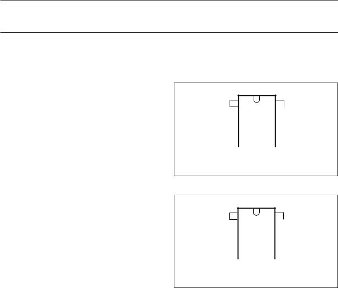
7.2Pin description PCF85103C-2
SYMBOL |
PIN |
DESCRIPTION |
|
|
|
WP |
1 |
address input 0 |
|
|
|
A1 |
2 |
address input 1 |
|
|
|
A2 |
3 |
address input 2 |
|
|
|
VSS |
4 |
negative supply voltage |
SDA |
5 |
serial data input/output (I2C-bus) |
SCL |
6 |
serial clock input (I2C-bus) |
n.c. |
7 |
not connected |
|
|
|
VDD |
8 |
positive supply voltage |
handbook, halfpage
A0 |
1 |
|
8 |
VDD |
||
|
|
|
|
|
|
n.c. |
A1 |
2 |
7 |
||||
A2 |
|
|
PCF85102C-2 |
|
|
SCL |
|
|
|
|
|||
3 |
|
|
6 |
|||
VSS |
|
|
|
|
|
|
4 |
5 |
SDA |
||||
|
|
|
|
|
|
|
|
|
|
MGL968 |
|
||
Fig.2 Pin configuration PCF85102C-2.
handbook, halfpage
WP |
1 |
|
8 |
VDD |
||
|
|
|
|
|
|
n.c. |
A1 |
2 |
7 |
||||
A2 |
|
|
PCF85103C-2 |
|
|
SCL |
|
|
|
|
|||
3 |
6 |
|||||
VSS |
|
|
|
|
|
|
4 |
5 |
SDA |
||||
|
|
|
|
|
|
|
|
|
|
MGL969 |
|
||
Fig.3 Pin configuration PCF85103C-2.
2000 Feb 15 |
6 |
 Loading...