


Philips PCF1252-0P-F4, PCF1252-0T-F4, PCF1252-5P, PCF1252-5P-F4, PCF1252-5T-F4 Datasheet
...
INTEGRATED CIRCUITS
DATA SHEET
PCF1252-X family
Threshold detector and reset generator
Product specification |
1998 Apr 16 |
Supersedes data of 1996 Jan 23
File under Integrated Circuits, IC11
Philips Semiconductors |
Product specification |
|
|
Threshold detector and reset generator |
PCF1252-X family |
|
|
|
|
FEATURES
∙Very low current consumption, typically 10 μA
∙10 factory programmed threshold voltages available covering trip voltages from 4.75 to 2.55 V
∙±50 mV trip point accuracy over full temperature range
∙Variable RESET delay
∙RESET pulse polarity selection
∙Defined outputs at 0.6 V (typ.)
∙Comparator for second level detection (e.g. overvoltage detection)
∙Advance warning of power fail
∙Operating temperature range −40 to +85 °C.
ORDERING INFORMATION
GENERAL DESCRIPTION
The PCF1252-Xs are low-power CMOS voltage threshold detectors designed especially for supervision of microcontroller/microprocessor systems for detection of power-on/off conditions and generation of a system reset pulse. The PCF1252-X also provides a POWF (power fail) output which is activated at a precise factory-programmed trip point. A system RESET output has a built-in delay with duration determined by an external capacitor (CCT).
A second comparator (comparator 2) has been included to enable the possibility of a second monitoring point in the system.
TYPE NUMBER |
|
PACKAGE |
|
|
|
|
|
||
NAME |
DESCRIPTION |
VERSION |
||
|
||||
|
|
|
|
|
PCF1252-XP(1) |
DIP8 |
plastic dual in-line package; 8 leads (300 mil) |
SOT97-1 |
|
PCF1252-XT(1) |
SO8 |
plastic small outline package; 8 leads; body width 3.9 mm |
SOT96-1 |
Note
1. X = 0 to 9; depending on threshold voltage.
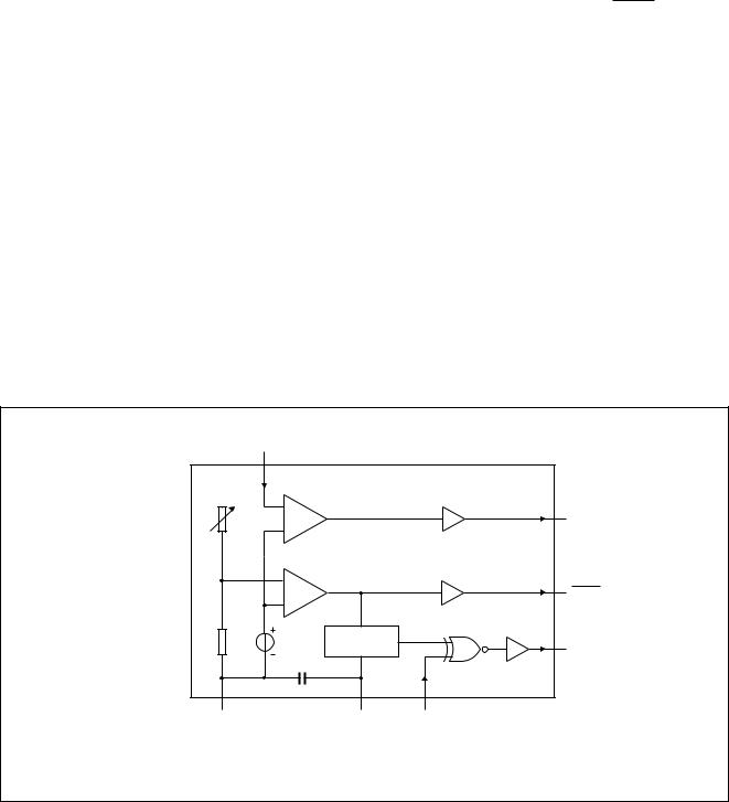
BLOCK DIAGRAM
handbook, full pagewidth |
VDD COMIN |
8 |
3 |
|
|
|
comparator 2 |
|
|
|
+ |
|
5 |
|
|
|
|
|
− |
|
COMOUT |
|
|
|
|
|
comparator 1 |
|
PCF1252-X |
|
+ |
|
7 |
|
|
|
|
|
− |
|
POWF |
|
|
|
|
|
1.30 V |
DELAY |
6 |
|
|
|
RESET |
4 |
|
1 |
2 |
|
|
|
MGC915 |
VSS |
|
CT |
SELECT |
Fig.1 Block diagram.
1998 Apr 16 |
2 |

Philips Semiconductors |
Product specification |
|
|
Threshold detector and reset generator |
PCF1252-X family |
|
|
PINNING
|
SYMBOL |
PIN |
DESCRIPTION |
|
|
|
|
|
|
|
CT |
1 |
connection for the external capacitor |
|
|
|
|
|
|
|
SELECT |
2 |
select polarity or external reset input |
|
|
|
|
|
|
|
COMIN |
3 |
comparator input |
|
|
|
|
|
|
|
VSS |
4 |
ground (0 V) |
|
|
COMOUT |
5 |
comparator output |
|
|
|
|
|
|
|
RESET |
6 |
reset output |
|
|
|
|
|
|
|
|
|
7 |
power failure signal output |
|
POWF |
|
||
|
|
|
|
|
|
VDD |
8 |
supply voltage |
|
FUNCTIONAL DESCRIPTION (see Fig.1)
The PCF1252-X contains:
∙A precise factory-programmed voltage reference
∙Two comparators
∙A delay circuit.
The PCF1252-X family is comprised of 10 versions with different factory-programmed voltage trip-points (VTRIP), see Chapter “Characteristics”.
Supply
The supply voltage (VDD) is internally divided before being compared, via comparator 1, with the internal reference voltage.
POWF (see Fig.3)
The POWF output is:
∙LOW, if VDD is below VTRIP
∙HIGH, if VDD is above VTRIP.
Power-on reset (SELECT = LOW)
As VDD rises past VTRIP, a positive reset pulse is generated at RESET. The duration of the reset pulse (tR) is determined by the value of the external capacitor (CCT; maximum 1 μF, see Fig.8) connected to CT. With no external capacitor connected, CCT assumes a minimum value of 100 pF. If SELECT is HIGH, the reset pulse is inverted.
Power failure
During a power-off condition (VDD < VTRIP), POWF goes LOW. After a time delay (tS), also determined by CCT,
RESET goes HIGH. Any POWF assertion (VDD < VTRIP) will result in a subsequent RESET pulse.
handbook, halfpage |
|
|
|
|
|
|
CT |
1 |
|
8 |
VDD |
||
SELECT |
2 |
|
|
|
|
|
PCF1252-X |
7 |
POWF |
||||
COMIN |
3 |
6 |
RESET |
|||
|
||||||
VSS |
4 |
|
5 |
COMOUT |
||
|
|
MGC916 |
|
|
||
Fig.2 Pinning diagram.
Voltage trip-point
By selecting the voltage trip-point slightly higher than the minimum operating voltage of the microcontroller/microprocessor, there is sufficient time for data storage before the power actually fails.
In order to prevent oscillations around the voltage trip-point, a small hysteresis has been included, resulting in a power-on switching point that is higher than the voltage trip-point (minimum of 15 mV). The voltage trip-point refers to the value at which power-off is signalled.
COMIN
Input to the second comparator (comparator 2).
When used in conjunction with an external voltage divider, this allows a second point in the system to be monitored. This input has no built-in hysteresis. When not in use connect to VDD. COMOUT will be LOW or HIGH depending on the voltage at COMIN:
∙COMOUT = HIGH, if voltage at COMIN is above the switch point VSP (typically 1.30 V).
∙COMOUT = LOW, if voltage at COMIN is below the switch point VSP (typically 1.30 V).
1998 Apr 16 |
3 |

Philips Semiconductors |
|
|
|
Product specification |
||
|
|
|
|
|
|
|
Threshold detector and reset generator |
|
PCF1252-X family |
||||
|
|
|
|
|
|
|
LIMITING VALUES |
|
|
|
|
|
|
In accordance with the Absolute Maximum Rating System (IEC 134). |
|
|
|
|
||
|
|
|
|
|
|
|
SYMBOL |
PARAMETER |
CONDITIONS |
MIN. |
|
MAX. |
UNIT |
|
|
|
|
|
|
|
VDD |
supply voltage |
|
−0.5 |
|
+7.0 |
V |
VI |
input voltage |
|
−0.5 |
|
VDD + 0.5 |
V |
II |
DC clamp-diode current |
all pins: VI < −0.5 V |
− |
|
20 |
mA |
|
|
or VI > VDD + 0.5 V |
|
|
|
|
IO |
output current |
|
− |
|
20 |
mA |
Ptot |
total power dissipation |
|
− |
|
150 |
mW |
Tstg |
storage temperature |
|
−65 |
|
+100 |
°C |
Tamb |
operating ambient temperature |
|
−40 |
|
+85 |
°C |
HANDLING
Inputs and outputs are protected against electrostatic discharge in normal handling. However, to be totally safe, it is desirable to take normal handling precautions appropriate to handling MOS devices (see “Handling MOS Devices”).
CHARACTERISTICS
VDD = 2.4 to 6.0 V; VSS = 0 V; Tamb = −40 to +85 °C; (see Fig.3); unless otherwise specified.
SYMBOL |
PARAMETER |
CONDITIONS |
MIN. |
TYP. |
MAX. |
UNIT |
|
|
|
|
|
|
|
VDD |
supply voltage |
|
2.4 |
− |
6.0 |
V |
VTRIP |
Voltage trip-point: |
Tamb = 25 °C; note 1 |
|
|
|
|
|
PCF1252-0 |
|
4.70 |
4.75 |
4.80 |
V |
|
PCF1252-1 |
|
4.50 |
4.55 |
4.60 |
V |
|
PCF1252-2 |
|
4.20 |
4.25 |
4.30 |
V |
|
PCF1252-3 |
|
4.00 |
4.05 |
4.10 |
V |
|
PCF1252-4 |
|
3.70 |
3.75 |
3.80 |
V |
|
PCF1252-5 |
|
3.50 |
3.55 |
3.60 |
V |
|
PCF1252-6 |
|
3.20 |
3.25 |
3.30 |
V |
|
PCF1252-7 |
|
3.00 |
3.05 |
3.10 |
V |
|
PCF1252-8 |
|
2.70 |
2.75 |
2.80 |
V |
|
PCF1252-9 |
|
2.50 |
2.55 |
2.60 |
V |
|
|
|
|
|
|
|
IDD |
supply current |
Tamb = 25 °C; |
− |
10 |
15 |
μA |
|
|
VDD = VTRIP + 0.5 V; |
|
|
|
|
|
|
COMIN = VDD; |
|
|
|
|
|
|
see Figs. 4 and 5 |
|
|
|
|
|
|
|
|
|
|
|
VTRIP |
voltage trip-point temperature |
note 2 |
− |
±100 × 10−6 |
±400 × 10−6 |
mV/K |
|
coefficient |
|
|
|
|
|
|
|
|
|
|
|
|
Vhys |
voltage trip-point hysteresis |
|
15 |
30 |
50 |
mV |
1998 Apr 16 |
4 |

Philips Semiconductors |
|
|
|
Product specification |
||||
|
|
|
|
|
|
|
|
|
|
Threshold detector and reset generator |
|
PCF1252-X family |
|||||
|
|
|
|
|
|
|
|
|
|
|
|
|
|
|
|
|
|
|
SYMBOL |
PARAMETER |
CONDITIONS |
MIN. |
TYP. |
MAX. |
UNIT |
|
|
|
|
|
|
|
|
|
|
|
COMIN |
|
|
|
|
|
|
|
|
|
|
|
|
|
|
|
|
|
VSP |
COMIN switch point |
Tamb = 25 °C; note 1 |
1.28 |
1.30 |
1.32 |
V |
|
|
VSP |
COMIN switch point temperature |
note 2 |
− |
±0.1 |
±0.5 |
mV/K |
|
|
|
|
coefficient |
|
|
|
|
|
|
|
|
|
|
|
|
|
|
|
SELECT |
|
|
|
|
|
|
|
|
|
|
|
|
|
|
|
|
|
VIL |
LOW level input voltage |
|
− |
− |
0.3VDD |
V |
|
|
VIH |
HIGH level input voltage |
|
0.7VDD |
− |
− |
V |
|
|
SELECT and COMIN |
|
|
|
|
|
||
|
|
|
|
|
|
|
|
|
|
ILI |
LOW level leakage input current |
|
− |
− |
−1.0 |
μA |
|
|
ILI |
HIGH level leakage input current |
|
− |
− |
1.0 |
μA |
|
|
|
RESET and COMOUT |
|
|
|
|
|
|
|
POWF, |
|
|
|
|
|
||
|
|
|
|
|
|
|
|
|
|
IO |
output sink current |
VO = 0.4 V; |
1 |
3 |
− |
mA |
|
|
|
|
|
VDD = 2.4 V; |
|
|
|
|
|
|
|
|
see Fig.6 |
|
|
|
|
|
|
|
|
|
|
|
|
|
|
IO |
output source current |
VO = 2.0 V; |
−0.75 |
−2 |
− |
mA |
|
|
|
|
|
VDD = 2.4 V; |
|
|
|
|
|
|
|
|
see Fig.7 |
|
|
|
|
|
|
|
|
|
|
|
|
|
|
tR |
reset time |
CCT = 1 nF; note 3 |
400 |
1000 |
2000 |
μs |
|
|
tS |
save time |
CCT = 1 nF; note 3 |
40 |
100 |
200 |
μs |
|
|
tR/tS |
reset to save time ratio |
|
− |
10 |
− |
|
|
|
Cint |
CT internal capacitance |
|
− |
100 |
− |
pF |
|
Notes
1.Long time stability of COMIN switch point VSP and voltage trip point VTRIP: within 10 years of continuous operation at VDD(max) and an average operating temperature of 55 °C the drift of VSP will not exceed ±10 mV. The maximum drift for VTRIP will not exceed (±VTRIP(typ)/VSP(typ)) 10 mV.
2.Values given per degree Kelvin; tested on a sample basis.
3.Conformance to these specifications is only guaranteed if the slew rate of VDD is less than 25 V/ms.
1998 Apr 16 |
5 |
 Loading...