


NSC LM118WG-883, LM118MW8, JM38510-10107SP, JM38510-10107SH, JM38510-10107BP Datasheet
...March 1998
LM118/LM218/LM318
Operational Amplifiers
General Description
The LM118 series are precision high speed operational amplifiers designed for applications requiring wide bandwidth and high slew rate. They feature a factor of ten increase in speed over general purpose devices without sacrificing DC performance.
The LM118 series has internal unity gain frequency compensation. This considerably simplifies its application since no external components are necessary for operation. However, unlike most internally compensated amplifiers, external frequency compensation may be added for optimum performance. For inverting applications, feedforward compensation will boost the slew rate to over 150V/µs and almost double the bandwidth. Overcompensation can be used with the amplifier for greater stability when maximum bandwidth is not needed. Further, a single capacitor can be added to reduce the 0.1% settling time to under 1 µs.
The high speed and fast settling time of these op amps make them useful in A/D converters, oscillators, active filters,
sample and hold circuits, or general purpose amplifiers. These devices are easy to apply and offer an order of magnitude better AC performance than industry standards such as the LM709.
The LM218 is identical to the LM118 except that the LM218 has its performance specified over a −25ÊC to +85ÊC temperature range. The LM318 is specified from 0ÊC to +70ÊC.
Features
n15 MHz small signal bandwidth
nGuaranteed 50V/µs slew rate
nMaximum bias current of 250 nA
nOperates from supplies of ±5V to ±20V
nInternal frequency compensation
nInput and output overload protected
nPin compatible with general purpose op amps
Connection Diagram
Dual-In-Line Package |
Dual-In-Line Package |
DS007766-3
|
DS007766-24 |
|
Top View |
Top View |
|
Order Number LM118J-8/883 (Note 2), |
||
Order Number LM118J/883 (Note 2) |
||
LM318M or LM318N |
||
See NS Package Number J14A |
||
See NS Package Number J08A, M08A or N08B |
||
|
Amplifiers Operational LM118/LM218/LM318
© 1999 National Semiconductor Corporation |
DS007766 |
www.national.com |

Connection Diagram (Continued)
Metal Can Package
(Note 1)
DS007766-2
Top View
Order Number LM118H, LM118H/883 (Note 2),
LM218H or LM318H
See NS Package Number H08C
Note 1: Pin connections shown on schematic diagram and typical applications are for TO-5 package.
Note 2: Available per JM38510/10107.
www.national.com |
2 |

Absolute Maximum Ratings (Note 8)
If Military/Aerospace specified devices are required, please contact the National Semiconductor Sales Office/ Distributors for availability and specifications.
Supply Voltage |
±20V |
Power Dissipation (Note 3) |
500 mW |
Differential Input Current (Note 4) |
±10 mA |
Input Voltage (Note 5) |
±15V |
Output Short-Circuit Duration |
Continuous |
Operating Temperature Range |
|
LM118 |
−55ÊC to +125ÊC |
LM218 |
−25ÊC to +85ÊC |
LM318 |
0ÊC to +70ÊC |
Storage Temperature Range |
−65ÊC to +150ÊC |
Electrical Characteristics (Note 6)
Lead Temperature (Soldering, 10 sec.) |
|
Hermetic Package |
300ÊC |
Plastic Package |
260ÊC |
Soldering Information |
|
Dual-In-Line Package |
|
Soldering (10 sec.) |
260ÊC |
Small Outline Package |
|
Vapor Phase (60 sec.) |
215ÊC |
Infrared (15 sec.) |
220ÊC |
See AN-450 ªSurface Mounting Methods and Their Effect on Product Reliabilityº for other methods of soldering surface mount devices.
ESD Tolerance (Note 9) |
2000V |
Parameter |
Conditions |
LM118/LM218 |
|
LM318 |
|
Units |
|||
|
|
|
|
|
|
|
|
|
|
|
|
Min |
Typ |
Max |
Min |
|
Typ |
Max |
|
|
|
|
|
|
|
|
|
|
|
Input Offset Voltage |
TA = 25ÊC |
|
2 |
4 |
|
|
4 |
10 |
mV |
Input Offset Current |
TA = 25ÊC |
|
6 |
50 |
|
|
30 |
200 |
nA |
Input Bias Current |
TA = 25ÊC |
|
120 |
250 |
|
|
150 |
500 |
nA |
Input Resistance |
TA = 25ÊC |
1 |
3 |
|
0.5 |
|
3 |
|
MW |
Supply Current |
TA = 25ÊC |
|
5 |
8 |
|
|
5 |
10 |
mA |
Large Signal Voltage Gain |
TA = 25ÊC, VS = ±15V |
50 |
200 |
|
25 |
|
200 |
|
V/mV |
|
VOUT = ±10V, RL ³ 2 kW |
|
|
|
|
|
|
|
|
Slew Rate |
TA = 25ÊC, VS = ±15V, AV = 1 |
50 |
70 |
|
50 |
|
70 |
|
V/µs |
|
(Note 7) |
|
|
|
|
|
|
|
|
|
|
|
|
|
|
|
|
|
|
Small Signal Bandwidth |
TA = 25ÊC, VS = ±15V |
|
15 |
|
|
|
15 |
|
MHz |
Input Offset Voltage |
|
|
|
6 |
|
|
|
15 |
mV |
|
|
|
|
|
|
|
|
|
|
Input Offset Current |
|
|
|
100 |
|
|
|
300 |
nA |
|
|
|
|
|
|
|
|
|
|
Input Bias Current |
|
|
|
500 |
|
|
|
750 |
nA |
|
|
|
|
|
|
|
|
|
|
Supply Current |
TA = 125ÊC |
|
4.5 |
7 |
|
|
|
|
mA |
Large Signal Voltage Gain |
VS = ±15V, VOUT = ±10V |
25 |
|
|
20 |
|
|
|
V/mV |
|
RL ³ 2 kW |
|
|
|
|
|
|
|
|
Output Voltage Swing |
VS = ±15V, RL = 2 kW |
±12 |
±13 |
|
±12 |
|
±13 |
|
V |
Input Voltage Range |
VS = ±15V |
±11.5 |
|
|
±11.5 |
|
|
|
V |
Common-Mode Rejection Ratio |
|
80 |
100 |
|
70 |
|
100 |
|
dB |
|
|
|
|
|
|
|
|
|
|
Supply Voltage Rejection Ratio |
|
70 |
80 |
|
65 |
|
80 |
|
dB |
|
|
|
|
|
|
|
|
|
|
Note 3: The maximum junction temperature of the LM118 is 150ÊC, the LM218 is 110ÊC, and the LM318 is 110ÊC. For operating at elevated temperatures, devices in the H08 package must be derated based on a thermal resistance of 160ÊC/W, junction to ambient, or 20ÊC/W, junction to case. The thermal resistance of the dual-in-line package is 100ÊC/W, junction to ambient.
Note 4: The inputs are shunted with back-to-back diodes for overvoltage protection. Therefore, excessive current will flow if a differential input voltage in excess of 1V is applied between the inputs unless some limiting resistance is used.
Note 5: For supply voltages less than ±15V, the absolute maximum input voltage is equal to the supply voltage.
Note 6: These specifications apply for ±5V ≤ VS ≤ ±20V and −55ÊC ≤ TA ≤ +125ÊC (LM118), −25ÊC ≤ TA ≤ +85ÊC (LM218), and 0ÊC ≤ TA ≤ +70ÊC (LM318). Also, power supplies must be bypassed with 0.1 µF disc capacitors.
Note 7: Slew rate is tested with VS = ±15V. The LM118 is in a unity-gain non-inverting configuration. VIN is stepped from −7.5V to +7.5V and vice versa. The slew rates between −5.0V and +5.0V and vice versa are tested and guaranteed to exceed 50V/µs.
Note 8: Refer to RETS118X for LM118H and LM118J military specifications.
Note 9: Human body model, 1.5 kΩ in series with 100 pF.
3 |
www.national.com |

Typical Performance Characteristics LM118, LM218
Input Current |
Voltage Gain |
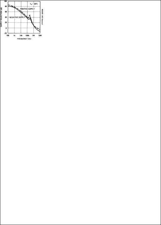
Power Supply Rejection |
DS007766-25 DS007766-26 DS007766-27
Input Noise Voltage Common Mode Rejection Supply Current
DS007766-28 DS007766-29 DS007766-30
Closed Loop Output |
Current Limiting |
Input Current |
Impedance |
|
|
DS007766-32 |
DS007766-33 |
DS007766-31 |
|
Unity Gain Bandwidth Voltage Follower Slew Rate Inverter Settling Time
DS007766-34 |
DS007766-35 |
DS007766-36 |
www.national.com |
4 |
Typical Performance Characteristics LM118, LM218 (Continued)
Large Signal Frequency |
Open Loop Frequency |
Voltage Follower Pulse |
Response |
Response |
Response |
DS007766-37 |
|
DS007766-38 |
DS007766-39 |
|
|
|
|
Large Signal Frequency |
Open Loop Frequency |
|
Inverter Pulse Response |
Response |
Response |
|
|
DS007766-42
DS007766-40
DS007766-41
Typical Performance Characteristics LM318
Input Current |
Voltage Gain |
Power Supply Rejection |
DS007766-43 |
DS007766-44 |
DS007766-45 |
5 |
www.national.com |
 Loading...