


LM2479NA
LM2479
120V Triple Bias Clamp
LM2479 120V Triple Bias Clamp
October 2000
General Description
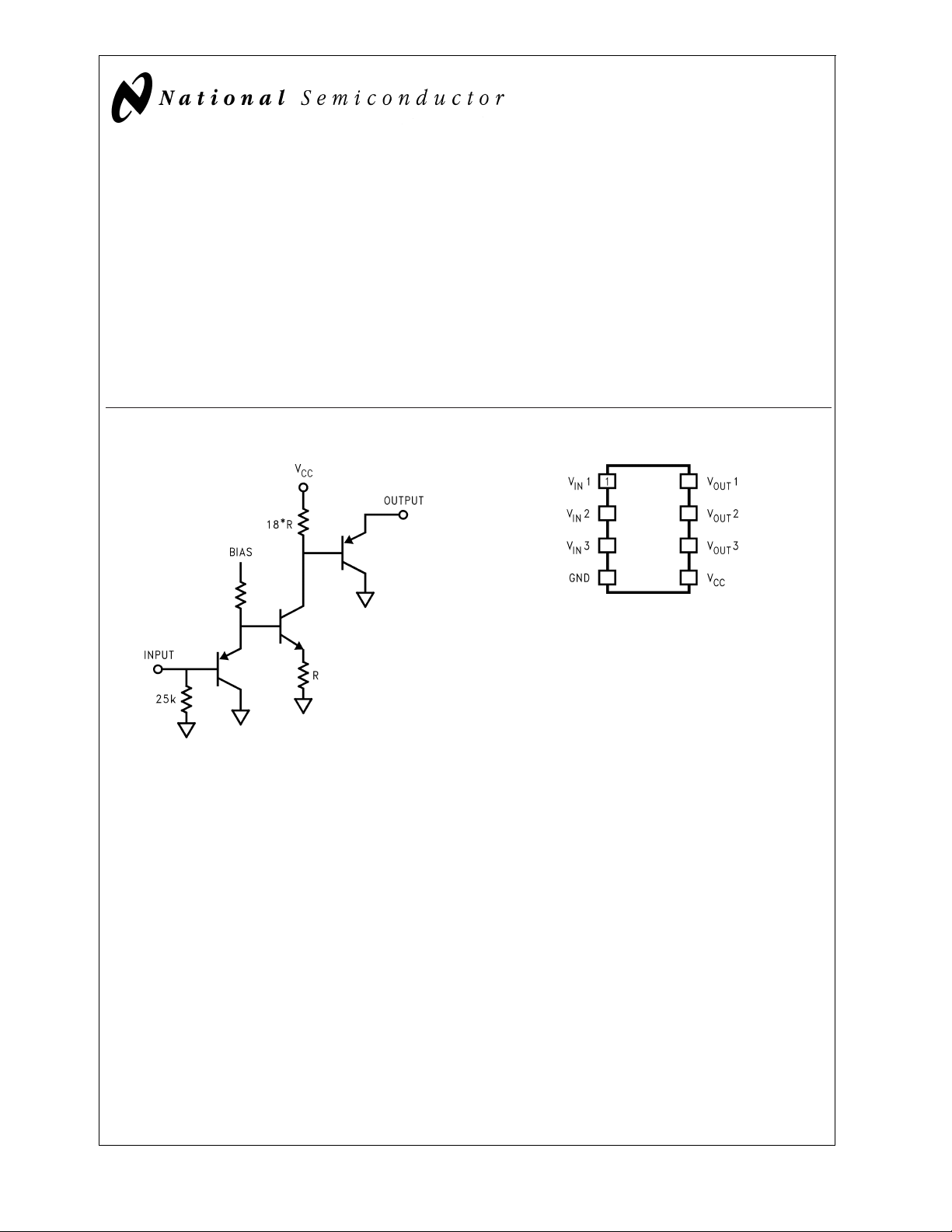
The LM2479 is an Integrated 120V triple bias clamp circuit
for DC recovery of each of the AC coupled outputs of a CRT
driver. It is well matched with the DAC outputs of the
LM126X family of pre-amplifiers. Each amplifier has its gain
internally set to -18. The IC is packaged in an industry
standard 8 lead molded DIP package.
n High input impedance
n Single supply operation
n Matched to the LM126X family of preamplifiers
Recommended Applications
n CRT monitors requiring DC restoration at the cathodes
Features
n Wide range integrated triple bias clamp
Block Diagrams Package Pinout
FIGURE 2. LM2479 Package Pinout
Order Number LM2479NA
NS Package Number: N08E
DS101391-2
DS101391-1
FIGURE 1. Simplified Schematic (One Channel)
© 2000 National Semiconductor Corporation DS101391 www.national.com
Absolute Maximum Ratings (Note 1)
If Military/Aerospace specified devices are required,
LM2479
please contact theNational Semiconductor Sales Office/
Distributors for availability and specifications.
Supply Voltage, V
Input Voltage, V
Storage Temperature Range, T
CC
IN
STG
-65˚C to +150˚C
+130V
0V to 5V
ESD Tolerance, Machine Model 200V
Limits of Operating Ranges (Note 3)
V
CC
V
OUT,VCC
= 120V 50 to 120V
Ambient Temperature Range, T
A
110 to 125
Lead Temperature (Soldering,
<
10sec.) 300˚C
DC CLAMP ELECTRICAL CHARACTERISTICS TARGETS AND LIMIT
Unless otherwise noted: VCC= +120V, VIN= 2.25VDC,TA= 25˚C.
Symbol Spec Parameter Conditions Min Typ Max Units
I
CC
V
OUT
V
OUT-Range
A
V
LE Linearity Error See Note 1 5 %
R
IN
Note 1: Linearity Error is the variation in DC gain from VIN= 1.0V to VIN= 4.0V.
Note 2: Absolute Maximum Ratings indicate limits beyond which damage to the device may occur.
Note 3: Operating Ratings indicate conditions for which the device is functional, but do not guarantee specific performance limits. For guaranteed specifications and
the test conditions, see the Electrical Characteristics. The guaranteed specifications apply only for the test conditions listed. Some performance characteristics may
change when the device is not operated under the listed test conditions.
Note 4: All voltages are measured with respect to GND, unless otherwise specified.
Supply Current All channels 2.3 3.5 mA
DC Output Voltage 83 87 91 V
Output Voltage Range VINRange = 1.0V - 4.0V 53 V
DC Voltage Gain -16 -18 -20
Input Resistance 24K Ω
0 to 70˚C
DC
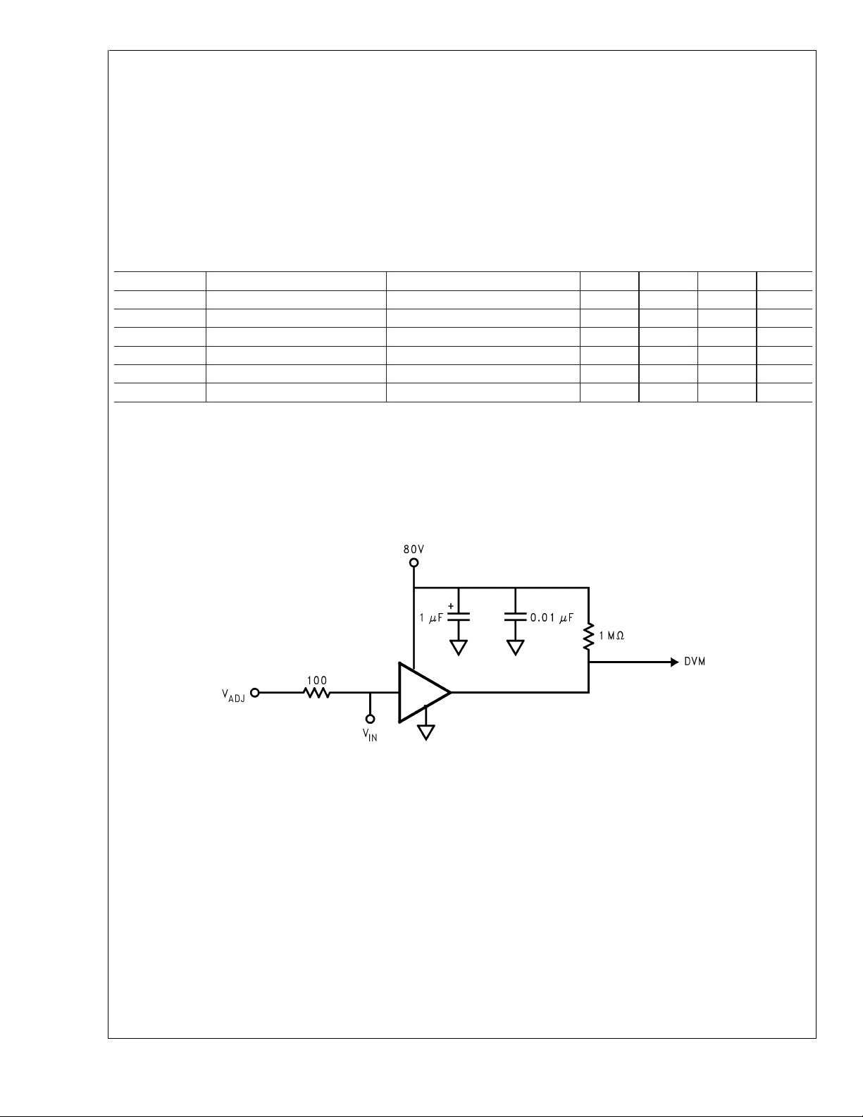
Test Circuit
Figure 3
measurements at the output.
shows the test circuit for evaluation of the LM2479 Clamp Amplifier. A high impedance VM (>100MΩ) is used for DC
DS101391-3
FIGURE 3. Test Circuit (One Channel)
www.national.com 2
 Loading...