


LM2439T
LM2439
Monolithic Triple 9.5 ns CRT Driver
General Description
The LM2439 is an integrated high voltage CRT driver circuit
designed for use in color monitor applications. The IC con-
tains three high input impedance, wide band amplifiers
which directly drivethe RGB cathodes of a CRT. Each chan-
nel has its gain internally set to −14 and can drive CRT ca-
pacitive loads as well as resistive loads present in other ap-
plications, limited only by the package’s power dissipation.
The IC is packaged in an industry standard 9-lead TO-220
molded plastic power package. See Thermal Considerations
section.
Features
n Dissipates approximately 50
%
less power than the
LM2406
n Well matched with LM1279 video preamp
n 0V to 5V input range
n Stable with 0 pF–20 pF capacitive loads and inductive
peaking networks
n Convenient TO-220 staggered lead package style
n Standard LM243X Family Pinout which is designed for
easy PCB layout
Applications
n 1024 x 768 Displays up to 70 Hz Refresh
n Pixel clock frequencies up to 75 MHz
n Monitors using video blanking
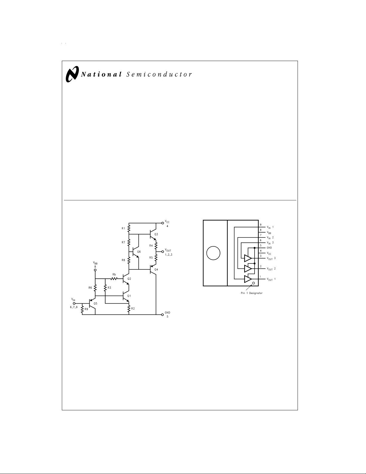
Schematic and Connection Diagrams
DS100988-1
FIGURE 1. Simplified Schematic Diagram
(One Channel)
DS100988-2
Note: TabisatGND
Top View
Order Number LM2439T
August 1999
LM2439 Monolithic Triple 9.5 ns CRT Driver
© 1999 National Semiconductor Corporation DS100988 www.national.com
Absolute Maximum Ratings (Notes 1, 3)
If Military/Aerospace specified devices are required,
please contact the National Semiconductor Sales Office/
Distributors for availability and specifications.
Supply Voltage, (V
CC
) +90V
Bias Voltage, (V
BB
) +16V
Input Voltage, (V
IN
) 0Vto6V
Storage Temperature Range, (T
STG
) −65˚C to +150˚C
Lead Temperature
(Soldering,
<
10 sec.) 300˚C
ESD Tolerance, Human Body Model 2 kV
Machine Model 250V
Operating Range (Note 2)
V
CC
+60V to +85V
V
BB
+8V to +15V
V
IN
+0V to +5V
V
OUT
+15V to +75V
Case Temperature −20˚C to +115˚C
Do not operate the part without a heat sink.
Electrical Characteristics
(See
Figure 2
for Test Circuit)
Unless otherwise noted: V
CC
= +80V, V
BB
= +12V, V
IN
= +2.7 V
DC
,C
L
= 8 pF, Output = 40 V
PP
at 1 MHz, T
C
= 50˚C.
Symbol Parameter Condition
LM2439
Units
Min Typ Max
I
CC
Supply Current Per Channel, No Input Signal, No
Output Load
8mA
I
BB
Bias Current All Three Channels 12 mA
V
OUT
DC Output Voltage No AC Input Signal, V
IN
= 1.2V 62 65 68 V
DC
A
V
DC Voltage Gain No AC Input Signal −12 −14 −16
∆A
V
Gain Matching (Note 4), No AC Input Signal 1.0 dB
LE Linearity Error (Notes 4, 5), No AC Input Signal 8
%
t
R
Rise Time (Note 6), 10
%
to 90
%
9ns
t
F
Fall Time (Note 6), 90
%
to 10
%
11 ns
OS Overshoot (Note 6) 1
%
Note 1: Absolute Maximum Ratings indicate limits beyond which damage to the device may occur.
Note 2: Operating ratings indicate conditions for which the device is functional, but do not guarantee specific performance limits. For guaranteed specifications and
test conditions, see the Electrical Characteristics. The guaranteed specifications apply only for the test conditions listed. Some performance characteristics may
change when the device is not operated under the listed test conditions.
Note 3: All voltages are measured with respect to GND, unless otherwise specified.
Note 4: Calculated value from Voltage Gain test on each channel.
Note 5: Linearity Error is the variation in dc gain from V
IN
= 1.0V to V
IN
= 4.5V.
Note 6: Input from signal generator: t
r
,t
f
<
1 ns.
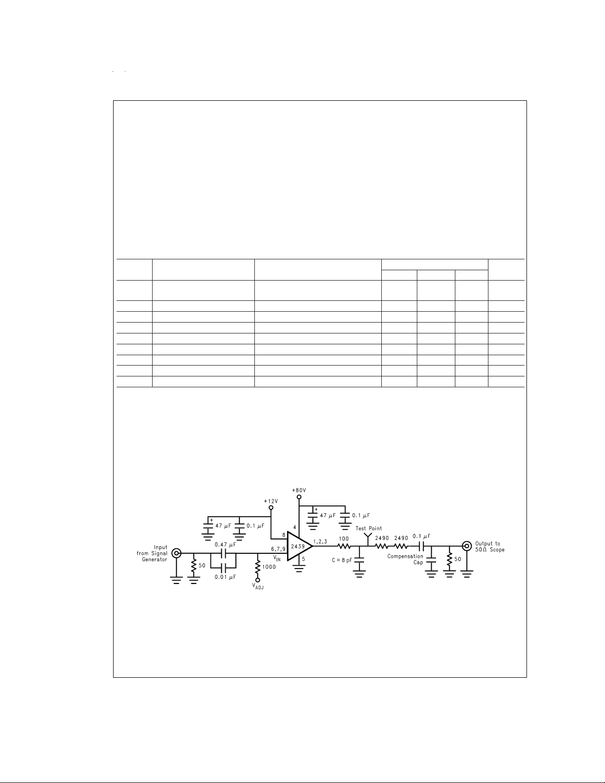
AC Test Circuit
Figure 2
shows a typical test circuit for evaluation of the LM2439. This circuit is designed to allow testing of the LM2439 in a 50Ω
environment without the use of an expensive FET probe. The two 2490Ω resistors form a 200:1 divider with the 50Ω resistor and
the oscilloscope. A test point is included for easy use of an oscilloscope probe. The compensation capacitor is used to compen-
sate the stray capacitance of the two 2490Ω resistors to achieve flat frequency response.
DS100988-3
Note: 8 pF load includes parasitic capacitance.
FIGURE 2. Test Circuit (One Channel)
www.national.com 2
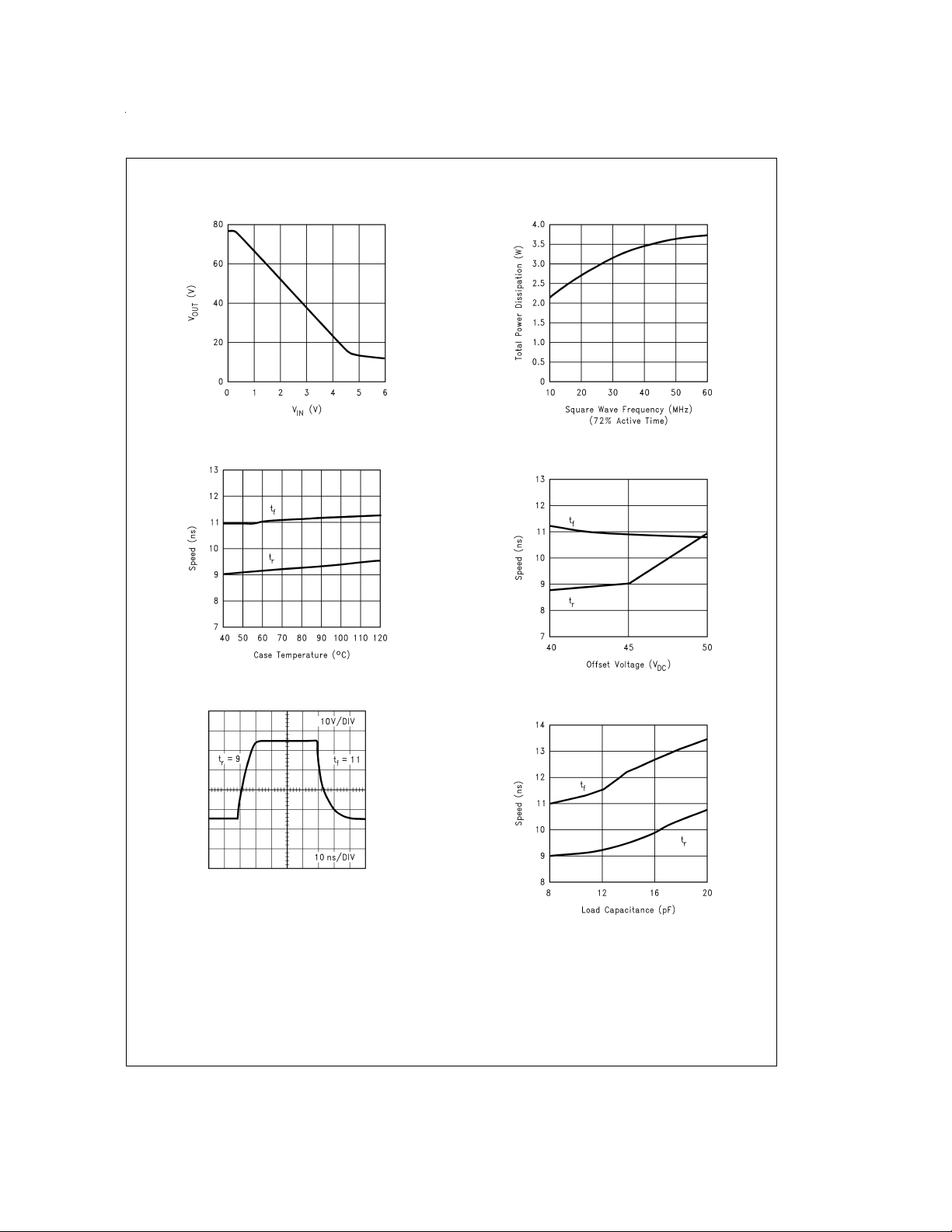
Typical Performance Characteristics (V
CC
= 80V, V
BB
= 12V, C
L
= 8pF, V
OUT
= 40V
PP
(25V-65V),
Test Circuit -
Figure 2
unless otherwise specified)
DS100988-4
FIGURE 3. V
OUT
vs V
IN
DS100988-5
FIGURE 4. Speed vs Temperature
DS100988-6
FIGURE 5. LM2439 Pulse Response
DS100988-7
FIGURE 6. Power Dissipation vs Frequency
DS100988-8
FIGURE 7. Speed vs Offset
DS100988-9
FIGURE 8. Speed vs Load Capacitance
www.national.com3
 Loading...