


NSC LM137HMDS, LM137HMDA, LM137H, LM137KMDA, LM137KGMD8 Datasheet
...May 1999
LM137/LM337
3-Terminal Adjustable Negative Regulators
General Description
The LM137/LM337 are adjustable 3-terminal negative voltage regulators capable of supplying in excess of −1.5A over an output voltage range of −1.2V to −37V. These regulators are exceptionally easy to apply, requiring only 2 external resistors to set the output voltage and 1 output capacitor for frequency compensation. The circuit design has been optimized for excellent regulation and low thermal transients. Further, the LM137 series features internal current limiting, thermal shutdown and safe-area compensation, making them virtually blowout-proof against overloads.
The LM137/LM337 serve a wide variety of applications including local on-card regulation, programmable-output voltage regulation or precision current regulation. The LM137/ LM337 are ideal complements to the LM117/LM317 adjustable positive regulators.
Features
nOutput voltage adjustable from −1.2V to −37V
n1.5A output current guaranteed, −55ÊC to +150ÊC
nLine regulation typically 0.01%/V
nLoad regulation typically 0.3%
nExcellent thermal regulation, 0.002%/W
n77 dB ripple rejection
nExcellent rejection of thermal transients
n50 ppm/ÊC temperature coefficient
nTemperature-independent current limit
nInternal thermal overload protection
nP+ Product Enhancement tested
nStandard 3-lead transistor package
nOutput is short circuit protected
LM137 Series Packages and Power
Capability
|
|
Rated |
Design |
Device |
Package |
Power |
Load |
|
|
Dissipation |
Current |
|
|
|
|
LM137/337 |
TO-3 (K) |
20W |
1.5A |
|
TO-39 (H) |
2W |
0.5A |
|
|
|
|
LM337 |
TO-220 (T) |
15W |
1.5A |
|
|
|
|
LM337 |
SOT-223 |
2W |
1A |
|
(MP) |
|
|
|
|
|
|
Typical Applications |
Comparison between SOT-223 and |
Adjustable Negative Voltage Regulator |
D-Pak (TO-252) Packages |
|
DS009067-31
Scale 1:1
DS009067-1
Full output current not available at high input-output voltages
²C1 = 1 µF solid tantalum or 10 µF aluminum electrolytic required for stability
*C2 = 1 µF solid tantalum is required only if regulator is more than 4" from power-supply filter capacitor
Output capacitors in the range of 1 µF to 1000 µF of aluminum or tantalum electrolytic are commonly used to provide improved output impedance and rejection of transients
Regulators Negative Adjustable Terminal-3 LM137/LM337
© 1999 National Semiconductor Corporation |
DS009067 |
www.national.com |

Absolute Maximum Ratings (Notes 1, 4)
If Military/Aerospace specified devices are required, please contact the National Semiconductor Sales Office/ Distributors for availability and specifications.
Power Dissipation |
Internally Limited |
Input-Output Voltage Differential |
40V |
Operating Junction Temperature Range |
|
LM137 |
−55ÊC to +150ÊC |
LM337 |
0ÊC to +125ÊC |
Storage Temperature |
−65ÊC to +150ÊC |
Lead Temperature (Soldering, 10 sec.) |
300ÊC |
Plastic Package (Soldering, 4 sec.) |
260ÊC |
ESD Rating |
2k Volts |
Electrical Characteristics
(Note 1)
Parameter |
Conditions |
|
LM137 |
|
LM337 |
|
Units |
|
|
|
|
|
|
|
|
|
|
|
|
Min |
Typ |
Max |
Min |
Typ |
Max |
|
|
|
|
|
|
|
|
|
|
Line Regulation |
Tj = 25ÊC, 3V ≤ |VIN − V OUT| ≤ 40V |
|
0.01 |
0.02 |
|
0.01 |
0.04 |
%/V |
|
(Note 2) IL = 10 mA |
|
|
|
|
|
|
|
Load Regulation |
Tj = 25ÊC, 10 mA ≤ IOUT ≤ IMAX |
|
0.3 |
0.5 |
|
0.3 |
1.0 |
% |
Thermal Regulation |
Tj = 25ÊC, 10 ms Pulse |
|
0.002 |
0.02 |
|
0.003 |
0.04 |
%/W |
Adjustment Pin Current |
|
|
65 |
100 |
|
65 |
100 |
µA |
|
|
|
|
|
|
|
|
|
Adjustment Pin Current Charge |
10 mA ≤ IL ≤ IMAX |
|
2 |
5 |
|
2 |
5 |
µA |
|
3.0V ≤ |VIN − V OUT| ≤ 40V, |
|
|
|
|
|
|
|
|
TA = 25ÊC |
|
|
|
|
|
|
|
Reference Voltage |
Tj = 25ÊC (Note 3) |
−1.225 |
−1.250 |
−1.275 |
−1.213 −1.250 −1.287 |
V |
||
|
3V ≤ |VIN − V OUT| ≤ 40V, (Note 3) |
−1.200 |
−1.250 |
−1.300 |
−1.200 |
−1.250 −1.300 |
V |
|
|
10 mA ≤ IOUT ≤ IMAX, P ≤ PMAX |
|
|
|
|
|
|
|
Line Regulation |
3V ≤ |VIN − V OUT| ≤ 40V, (Note 2) |
|
0.02 |
0.05 |
|
0.02 |
0.07 |
%/V |
Load Regulation |
10 mA ≤ IOUT ≤ IMAX, (Note 2) |
|
0.3 |
1 |
|
0.3 |
1.5 |
% |
Temperature Stability |
TMIN ≤ Tj ≤ TMAX |
|
0.6 |
|
|
0.6 |
|
% |
Minimum Load Current |
|VIN − V OUT| ≤ 40V |
|
2.5 |
5 |
|
2.5 |
10 |
mA |
|
|VIN − V OUT| ≤ 10V |
|
1.2 |
3 |
|
1.5 |
6 |
mA |
Current Limit |
|VIN − V OUT| ≤ 15V |
|
|
|
|
|
|
|
|
K, MP and T Package |
1.5 |
2.2 |
3.5 |
1.5 |
2.2 |
3.7 |
A |
|
H Package |
0.5 |
0.8 |
1.8 |
0.5 |
0.8 |
1.9 |
A |
|
|VIN − V OUT| = 40V, Tj = 25ÊC |
|
|
|
|
|
|
|
|
K, MP and T Package |
0.24 |
0.4 |
|
0.15 |
0.4 |
|
A |
|
H Package |
0.15 |
0.17 |
|
0.10 |
0.17 |
|
A |
|
|
|
|
|
|
|
|
|
RMS Output Noise, % of VOUT |
Tj = 25ÊC, 10 Hz ≤ f ≤ 10 kHz |
|
0.003 |
|
|
0.003 |
|
% |
Ripple Rejection Ratio |
VOUT = −10V, f = 120 Hz |
|
60 |
|
|
60 |
|
dB |
|
CADJ = 10 µF |
66 |
77 |
|
66 |
77 |
|
dB |
Long-Term Stability |
Tj = 125ÊC, 1000 Hours |
|
0.3 |
1 |
|
0.3 |
1 |
% |
Thermal Resistance, Junction to |
H Package |
|
12 |
15 |
|
12 |
15 |
ÊC/W |
Case |
K Package |
|
2.3 |
3 |
|
2.3 |
3 |
ÊC/W |
|
T Package |
|
|
|
|
4 |
|
ÊC/W |
|
|
|
|
|
|
|
|
|
Thermal Resistance, Junction to |
H Package |
|
140 |
|
|
140 |
|
ÊC/W |
Ambient (No Heat Sink) |
K Package |
|
35 |
|
|
35 |
|
ÊC/W |
|
T Package |
|
|
|
|
50 |
|
ÊC/W |
|
MP Package |
|
|
|
|
170 |
|
ÊC/W |
|
|
|
|
|
|
|
|
|
Note 1: Unless otherwise specified, these specifications apply −55ÊC ≤ Tj ≤ +150ÊC for the LM137, 0ÊC ≤ Tj ≤ +125ÊC for the LM337; VIN − V OUT = 5V; and IOUT = 0.1A for the TO-39 package and IOUT = 0.5A for the TO-3, SOT-223 and TO-220 packages. Although power dissipation is internally limited, these specifications
are applicable for power dissipations of 2W for the TO-39 and SOT-223 (see Application Hints), and 20W for the TO-3, and TO-220. IMAX is 1.5A for the TO-3, SOT-223 and TO-220 packages, and 0.2A for the TO-39 package.
Note 2: Regulation is measured at constant junction temperature, using pulse testing with a low duty cycle. Changes in output voltage due to heating effects are covered under the specification for thermal regulation. Load regulation is measured on the output pin at a point 1¤8" below the base of the TO-3 and TO-39 packages.
Note 3: Selected devices with tightened tolerance reference voltage available.
Note 4: Refer to RETS137H drawing for LM137H or RETS137K drawing for LM137K military specifications.
www.national.com |
2 |

Schematic Diagram
Thermal Regulation
When power is dissipated in an IC, a temperature gradient occurs across the IC chip affecting the individual IC circuit components. With an IC regulator, this gradient can be especially severe since power dissipation is large. Thermal regulation is the effect of these temperature gradients on output voltage (in percentage output change) per Watt of power change in a specified time. Thermal regulation error is independent of electrical regulation or temperature coefficient, and occurs within 5 ms to 50 ms after a change in power dissipation. Thermal regulation depends on IC layout as well as electrical design. The thermal regulation of a voltage regulator is defined as the percentage change of VOUT, per Watt, within the first 10 ms after a step of power is applied. The LM137's specification is 0.02%/W, max.
DS009067-2
DS009067-3
LM137, VOUT = −10V
VIN − V OUT = −40V
IIL = 0A → 0.25A → 0A
Vertical sensitivity, 5 mV/div
FIGURE 1.
In Figure 1, a typical LM137's output drifts only 3 mV (or 0.03% of VOUT = −10V) when a 10W pulse is applied for 10 ms. This performance is thus well inside the specification limit of 0.02%/W x 10W = 0.2% max. When the 10W pulse is ended, the thermal regulation again shows a 3 mV step at the LM137 chip cools off. Note that the load regulation error of about 8 mV (0.08%) is additional to the thermal regulation error. In Figure 2, when the 10W pulse is applied for 100 ms, the output drifts only slightly beyond the drift in the first 10 ms, and the thermal error stays well within 0.1% (10 mV).
3 |
www.national.com |
Thermal Regulation (Continued)
TO-220
Plastic Package
DS009067-4
LM137, VOUT = −10V
VIN − V OUT = −40V
IL = 0A → 0.25A → 0A
Horizontal sensitivity, 20 ms/div
FIGURE 2.
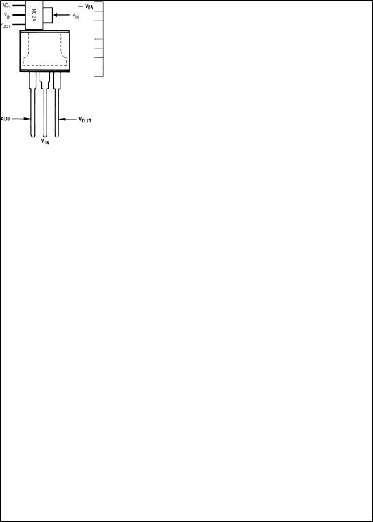
Connection Diagrams
TO-3
Metal Can Package
DS009067-5
Case is Input
Bottom View
Order Number LM137K/883
LM137KPQML and LM137KPQMLV(Note 5)
See NS Package Number K02C
Order Number LM337K STEEL
See NS Package Number K02A
TO-39
Metal Can Package
DS009067-6
Case Is Input
Note 5: See STD Mil DWG 5962P99517 for Radiation Tolerant Devices
Bottom View
Order Number LM137H, LM137H/883 or LM337H LM137HPQML and LM137HPQMLV(Note 5)
See NS Package Number H03A
DS009067-7
Front View
Order Number LM337T
See NS Package Number T03B
3-Lead SOT-223
DS009067-34
Front View
Order Number LM337IMP
Package Marked N02ASee NS Package Number MA04A
Application Hints
When a value for θ(H−A) is found using the equation shown, a heatsink must be selected that has a value that is less than
or equal to this number.
HEATSINKING SOT-223 PACKAGE PARTS
The SOT-223 (ªMPº) packages use a copper plane on the PCB and the PCB itself as a heatsink. To optimize the heat sinking ability of the plane and PCB, solder the tab of the package to the plane.
Figures 3, 4 show the information for the SOT-223 package.
Figure 4 assumes a θ(J−A) of 75ÊC/W for 1 ounce copper and 51ÊC/W for 2 ounce copper and a maximum junction tem-
perature of 125ÊC.
www.national.com |
4 |
 Loading...