


LM2574HVM-ADJ
NSC LM2574HVM-ADJ, LM2574HVM-5.0, LM2574HVM-3.3, LM2574HVM-12, LM2574HVN-3.3 Datasheet
...
LM2574/LM2574HV
SIMPLE SWITCHER
™
0.5A Step-Down Voltage Regulator
General Description
The LM2574 series of regulators are monolithic integrated
circuits that provide all the active functions for a step-down
(buck) switching regulator, capable of driving a 0.5A load
with excellent line and load regulation. These devices are
available in fixed output voltages of 3.3V, 5V, 12V, 15V, and
an adjustable output version.
Requiring aminimumnumber of external components, these
regulators are simple to use and include internal frequency
compensation and a fixed-frequency oscillator.
The LM2574 series offers a high-efficiency replacement for
popular three-terminal linear regulators. Because of its high
efficiency, the copper traces on the printed circuit board are
normally the only heat sinking needed.
A standard series of inductors optimized for use with the
LM2574 are available from several different manufacturers.
This feature greatly simplifies the design of switch-mode
power supplies.
Other features include a guaranteed
±
4%tolerance on output voltage within specified input voltages and output load
conditions, and
±
10%on the oscillator frequency. External
shutdown is included, featuring 50 µA (typical) standby current. The output switch includes cycle-by-cycle current limiting, as well as thermal shutdown for full protection under
fault conditions.
Features
n 3.3V, 5V, 12V, 15V, and adjustable output versions
n Adjustable version output voltage range, 1.23V to 37V
(57V for HV version)
±
4%max over line and load
conditions
n Guaranteed 0.5A output current
n Wide input voltage range, 40V, up to 60V for HV version
n Requires only 4 external components
n 52 kHz fixed frequency internal oscillator
n TTL shutdown capability, low power standby mode
n High efficiency
n Uses readily available standard inductors
n Thermal shutdown and current limit protection
Applications
n Simple high-efficiency step-down (buck) regulator
n Efficient pre-regulator for linear regulators
n On-card switching regulators
n Positive to negative converter (Buck-Boost)
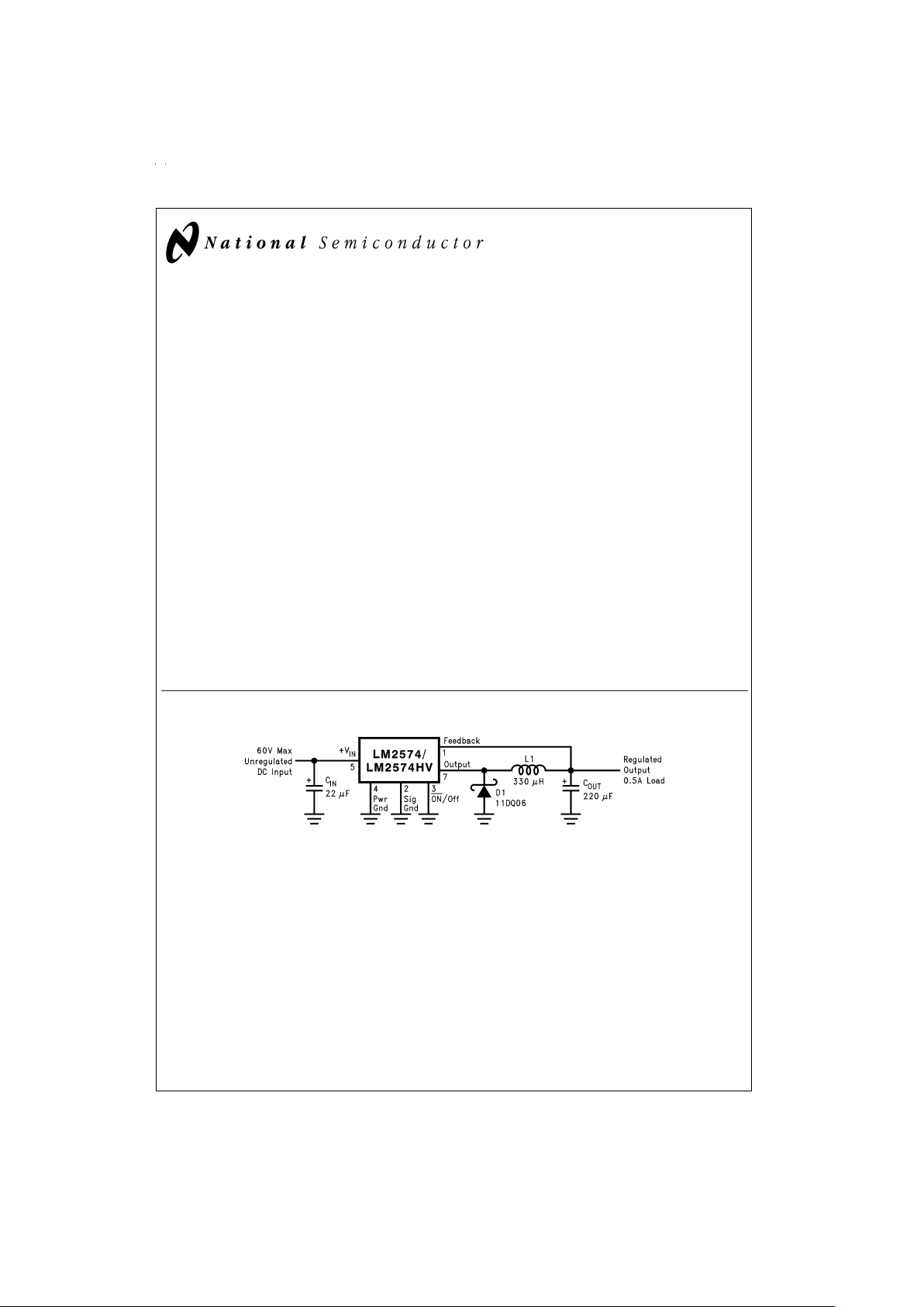
Typical Application (Fixed Output Voltage Versions)
Patent Pending
SIMPLE SWITCHER
™
is a trademark of National Semiconductor Corporation
DS011394-1
Note: Pin numbers are for 8-pin DIP package.
June 1999
LM2574/LM2574HV SIMPLE SWITCHER 0.5A Step-Down Voltage Regulator
© 1999 National Semiconductor Corporation DS011394 www.national.com
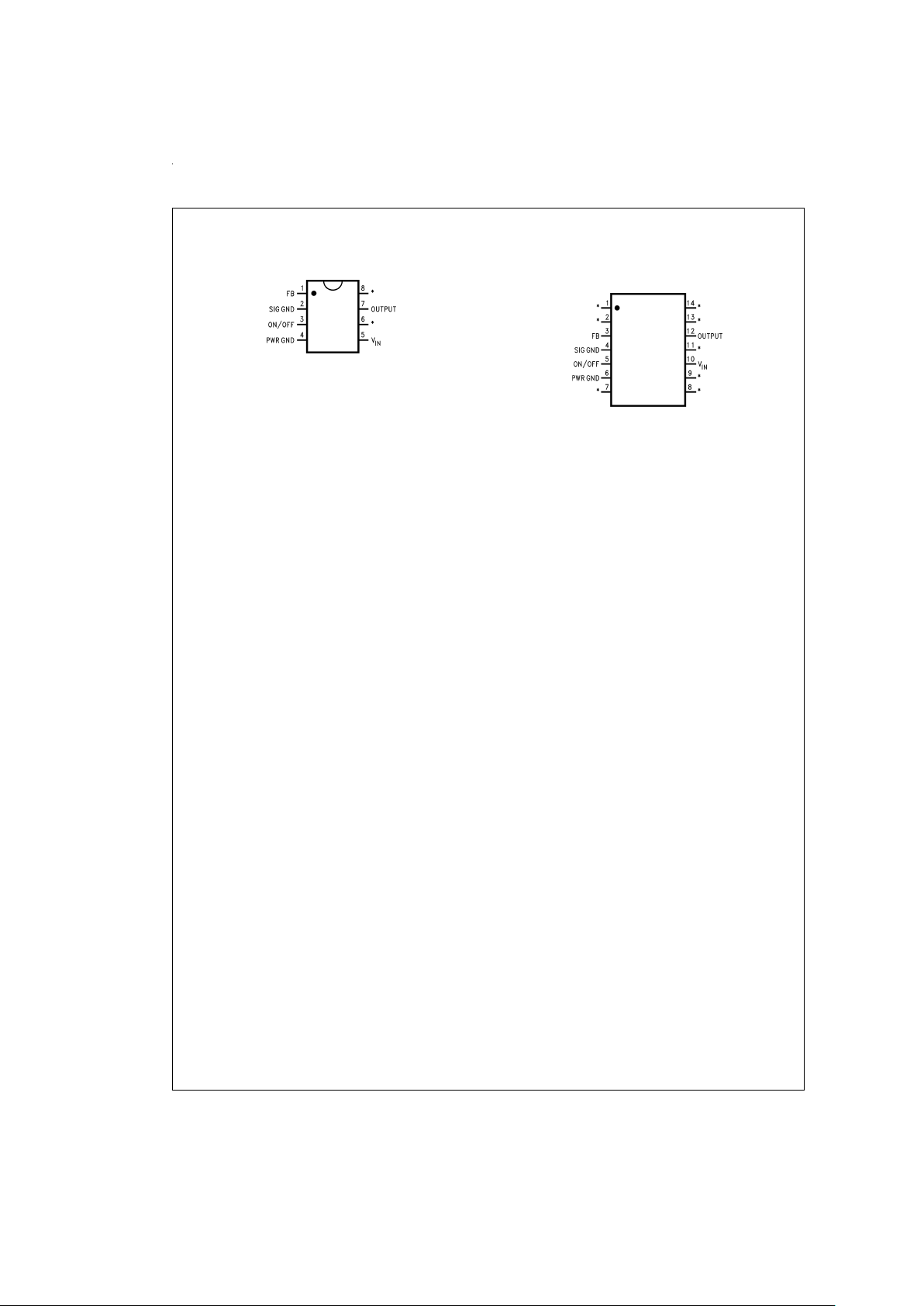
Connection Diagrams
8-Lead DIP
DS011394-2
* No internal connection, but should be soldered to PC board for best heat
transfer.
Top View
Order Number LM2574-3.3HVN, LM2574HVN-5.0,
LM2574HVN-12, LM2574HVN-15, LM2574HVN-ADJ,
LM2574N-3.3, LM2574N-5.0, LM2574N-12,
LM2574N-15 or LM2574N-ADJ
See NS Package Number N08A
14-Lead Wide
Surface Mount (WM)
DS011394-3
Top View
Order Number LM2574HVM-3.3, LM2574HVM-5.0,
LM2574HVM-12, LM2574HVM-15, LM2574HVM-ADJ,
LM2574M-3.3 LM2574M-5.0, LM2574M-12,
LM2574M-15 or LM2574M-ADJ
See NS Package Number M14B
www.national.com 2
Absolute Maximum Ratings (Note 1)
If Military/Aerospace specified devices are required,
please contact the National Semiconductor Sales Office/
Distributors for availability and specifications.
Maximum Supply Voltage
LM2574 45V
LM2574HV 63V
ON /OFF Pin Input Voltage
−0.3V ≤ V ≤ +V
IN
Output Voltage to Ground
(Steady State) −1V
Minimum ESD Rating
(C=100 pF, R=1.5 kΩ)2kV
Storage Temperature Range −65˚C to +150˚C
Lead Temperature
(Soldering, 10 seconds) 260˚C
Maximum Junction Temperature 150˚C
Power Dissipation Internally Limited
Operating Ratings
Temperature Range
LM2574/LM2574HV −40˚C ≤ T
J
≤ +125˚C
Supply Voltage
LM2574 40V
LM2574HV 60V
LM2574-3.3, LM2574HV-3.3
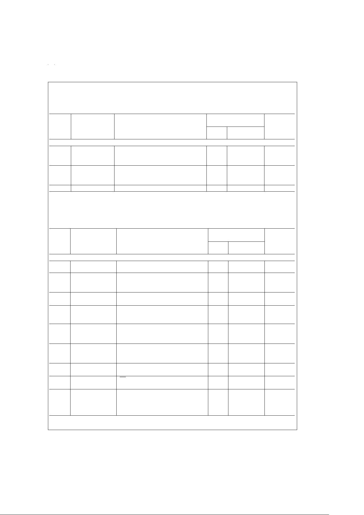
Electrical Characteristics
Specifications with standard type face are for T
J
=
25˚C, and those with boldface type apply over full Operating Tempera-
ture Range.
Symbol Parameter Conditions LM2574-3.3 Units
(Limits)
LM2574HV-3.3
Typ Limit
(Note 2)
SYSTEM PARAMETERS (Note 3) Test Circuit
Figure 2
V
OUT
Output Voltage V
IN
=
12V, I
LOAD
=
100 mA 3.3 V
3.234 V(Min)
3.366 V(Max)
V
OUT
Output Voltage 4.75V ≤ VIN≤ 40V, 0.1A ≤ I
LOAD
≤ 0.5A 3.3 V
LM2574 3.168/3.135 V(Min)
3.432/3.465 V(Max)
V
OUT
Output Voltage 4.75V ≤ VIN≤ 60V, 0.1A ≤ I
LOAD
≤ 0.5A 3.3
LM2574HV 3.168/3.135 V(Min)
3.450/3.482 V(Max)
η Efficiency V
IN
=
12V, I
LOAD
=
0.5A 72
%
LM2574-5.0, LM2574HV-5.0
Electrical Characteristics
Specifications with standard type face are for T
J
=
25˚C, and those with boldface type apply over full Operating Tempera-
ture Range.
Symbol Parameter Conditions LM2574-5.0 Units
(Limits)
LM2574HV-5.0
Typ Limit
(Note 2)
SYSTEM PARAMETERS (Note 3) Test Circuit
Figure 2
V
OUT
Output Voltage V
IN
=
12V, I
LOAD
=
100 mA 5 V
4.900 V(Min)
5.100 V(Max)
V
OUT
Output Voltage 7V ≤ VIN≤ 40V, 0.1A ≤ I
LOAD
≤ 0.5A 5 V
LM2574 4.800/4.750 V(Min)
5.200/5.250 V(Max)
V
OUT
Output Voltage 7V ≤ VIN≤ 60V, 0.1A ≤ I
LOAD
≤ 0.5A 5
LM2574HV 4.800/4.750 V(Min)
5.225/5.275 V(Max)
η Efficiency V
IN
=
12V, I
LOAD
=
0.5A 77
%
www.national.com3
LM2574-12, LM2574HV-12
Electrical Characteristics
Specifications with standard type face are for T
J
=
25˚C, and those with boldface type apply over full Operating Tempera-
ture Range.
Symbol Parameter Conditions LM2574-12 Units
(Limits)
LM2574HV-12
Typ Limit
(Note 2)
SYSTEM PARAMETERS (Note 3) Test Circuit
Figure 2
V
OUT
Output Voltage V
IN
=
25V, I
LOAD
=
100 mA 12 V
11.76 V(Min)
12.24 V(Max)
V
OUT
Output Voltage 15V ≤ VIN≤ 40V, 0.1A ≤ I
LOAD
≤ 0.5A 12 V
LM2574 11.52/11.40 V(Min)
12.48/12.60 V(Max)
V
OUT
Output Voltage 15V ≤ VIN≤ 60V, 0.1A ≤ I
LOAD
≤ 0.5A 12
LM2574HV 11.52/11.40 V(Min)
12.54/12.66 V(Max)
η Efficiency V
IN
=
15V, I
LOAD
=
0.5A 88
%
LM2574-15, LM2574HV-15
Electrical Characteristics
Specifications with standard type face are for T
J
=
25˚C, and those with boldface type apply over full Operating Tempera-
ture Range.
Symbol Parameter Conditions LM2574-15 Units
(Limits)
LM2574HV-15
Typ Limit
(Note 2)
SYSTEM PARAMETERS (Note 3) Test Circuit
Figure 2
V
OUT
Output Voltage V
IN
=
30V, I
LOAD
=
100 mA 15 V
14.70 V(Min)
15.30 V(Max)
V
OUT
Output Voltage 18V ≤ VIN≤ 40V, 0.1A ≤ I
LOAD
≤ 0.5A 15 V
LM2574 14.40/14.25 V(Min)
15.60/15.75 V(Max)
V
OUT
Output Voltage 18V ≤ VIN≤ 60V, 0.1A ≤ I
LOAD
≤ 0.5A 15
LM2574HV 14.40/14.25 V(Min)
15.68/15.83 V(Max)
η Efficiency V
IN
=
18V, I
LOAD
=
0.5A 88
%
LM2574-ADJ, LM2574HV-ADJ
Electrical Characteristics
Specifications with standard type face are for T
J
=
25˚C, and those with boldface type apply over full Operating Tempera-
ture Range. Unless otherwise specified, V
IN
=
12V, I
LOAD
=
100 mA.
Symbol Parameter Conditions LM2574-ADJ Units
(Limits)
LM2574HV-ADJ
Typ Limit
(Note 2)
SYSTEM PARAMETERS (Note 3) Test Circuit
Figure 2
V
FB
Feedback Voltage V
IN
=
12V, I
LOAD
=
100 mA 1.230 V
1.217 V(Min)
1.243 V(Max)
www.national.com 4
LM2574-ADJ, LM2574HV-ADJ
Electrical Characteristics
(Continued)
Specifications with standard type face are for T
J
=
25˚C, and those with boldface type apply over full Operating Tempera-
ture Range. Unless otherwise specified, V
IN
=
12V, I
LOAD
=
100 mA.
Symbol Parameter Conditions LM2574-ADJ Units
(Limits)
LM2574HV-ADJ
Typ Limit
(Note 2)
SYSTEM PARAMETERS (Note 3) Test Circuit
Figure 2
V
FB
Feedback Voltage 7V ≤ VIN≤ 40V, 0.1A ≤ I
LOAD
≤ 0.5A 1.230 V
LM2574 V
OUT
Programmed for 5V. Circuit of
Figure 2
1.193/1.180 V(Min)
1.267/1.280 V(Max)
V
FB
Feedback Voltage 7V ≤ VIN≤ 60V, 0.1A ≤ I
LOAD
≤ 0.5A 1.230
LM2574HV V
OUT
Programmed for 5V. Circuit of
Figure 2
1.193/1.180 V(Min)
1.273/1.286 V(Max)
η Efficiency V
IN
=
12V, V
OUT
=
5V, I
LOAD
=
0.5A 77
%
All Output Voltage Versions
Electrical Characteristics
Specifications with standard type face are for T
J
=
25˚C, and those with boldface type apply over full Operating Tempera-
ture Range. Unless otherwise specified, V
IN
=
12V for the 3.3V, 5V, and Adjustable version, V
IN
=
25V for the 12V version,
and V
IN
=
30V for the 15V version. I
LOAD
=
100 mA.
Symbol Parameter Conditions LM2574-XX Units
(Limits)
LM2574HV-XX
Typ Limit
(Note 2)
DEVICE PARAMETERS
I
b
Feedback Bias
Current
Adjustable Version Only, V
OUT
=
5V 50 100/500 nA
f
O
Oscillator Frequency (see Note 10) 52 kHz
47/42 kHz(Min)
58/63 kHz(Max)
V
SAT
Saturation Voltage I
OUT
=
0.5A (Note 4) 0.9 V
1.2/1.4 V(max)
DC Max Duty Cycle
(ON)
(Note 5) 98
%
93
%
(Min)
I
CL
Current Limit Peak Current, (Notes 4, 10) 1.0 A
0.7/0.65 A(Min)
1.6/1.8 A(Max)
I
L
Output Leakage (Notes 6, 7) Output=0V 2 mA(Max)
Current Output=−1V 7.5 mA
Output=−1V 30 mA(Max)
I
Q
Quiescent Current (Note 6) 5 mA
10 mA(Max)
I
STBY
Standby Quiescent ON /OFF Pin=5V (OFF) 50 µA
Current 200 µA(Max)
θ
JA
Thermal Resistance N Package, Junction to Ambient (Note 8) 92
θ
JA
N Package, Junction to Ambient (Note 9) 72 ˚C/W
θ
JA
M Package, Junction to Ambient (Note 8) 102
θ
JA
M Package, Junction to Ambient (Note 9) 78
www.national.com5
All Output Voltage Versions
Electrical Characteristics
(Continued)
Specifications with standard type face are for T
J
=
25˚C, and those with boldface type apply over full Operating Tempera-
ture Range. Unless otherwise specified, V
IN
=
12V for the 3.3V, 5V, and Adjustable version, V
IN
=
25V for the 12V version,
and V
IN
=
30V for the 15V version. I
LOAD
=
100 mA.
Symbol Parameter Conditions LM2574-XX Units
(Limits)
LM2574HV-XX
Typ Limit
(Note 2)
ON /OFF CONTROL Test Circuit
Figure 2
V
IH
ON /OFF Pin Logic V
OUT
=
0V 1.4 2.2/2.4 V(Min)
V
IL
Input Level V
OUT
=
Nominal Output Voltage 1.2 1.0/0.8 V(Max)
I
H
ON /OFF Pin Input ON /OFF Pin=5V (OFF) 12 µA
Current 30 µA(Max)
I
IL
ON /OFF Pin=0V (ON) 0µA
10 µA(Max)
Note 1: Absolute Maximum Ratings indicate limits beyond which damage to the device may occur.Operating Ratings indicate conditions for which the device is intended to be functional, but do not guarantee specific performance limits. For guaranteed specifications and test conditions, see the Electrical Characteristics.
Note 2: All limits guaranteed at room temperature (Standard type face) and at temperature extremes (bold type face). All room temperature limits are 100%produc-
tion tested. All limits at temperature extremes are guaranteed via correlation using standard Statistical Quality Control (SQC) methods. All limits are used to calculate
Average Outgoing Quality Level.
Note 3: External components such as the catch diode, inductor, input and output capacitors can affect switching regulator system performance. When the LM2574
is used as shown in the
Figure 2
test circuit, system performance will be as shown in system parameters section of Electrical Characteristics.
Note 4: Output pin sourcing current. No diode, inductor or capacitor connected to output pin.
Note 5: Feedback pin removed from output and connected to 0V.
Note 6: Feedback pin removed from output and connected to +12V for the Adjustable, 3.3V,and 5V versions, and +25V for the 12V and 15V versions, to force the
output transistor OFF.
Note 7: V
IN
=
40V (60V for high voltage version).
Note 8: Junction to ambient thermal resistance with approximately 1 square inch of printed circuit board copper surrounding the leads. Additional copper area will
lower thermal resistance further. See application hints in this data sheet and the thermal model in Switchers Made Simple software.
Note 9: Junction to ambient thermal resistance with approximately 4 square inches of 1 oz. (0.0014 in. thick) printed circuit board copper surrounding the leads. Additional copper area will lower thermal resistance further. (See Note 8.)
Note 10: The oscillator frequency reduces to approximately 18 kHz in the event of an output short or an overload which causes the regulated output voltage to drop
approximately 40%from the nominal output voltage. This self protection feature lowers the average power dissipation of the IC by lowering the minimum duty cycle
from 5%down to approximately 2%.
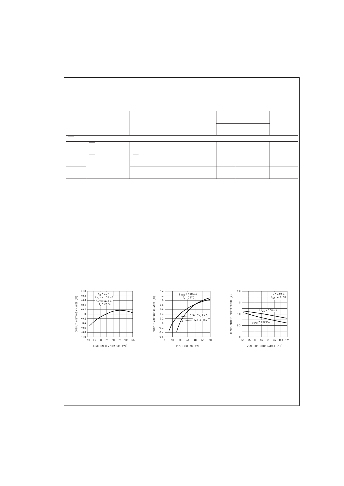
Typical Performance Characteristics (Circuit of
Figure 2
)
Normalized Output Voltage
DS011394-27
Line Regulation
DS011394-28
Dropout Voltage
DS011394-29
www.national.com 6
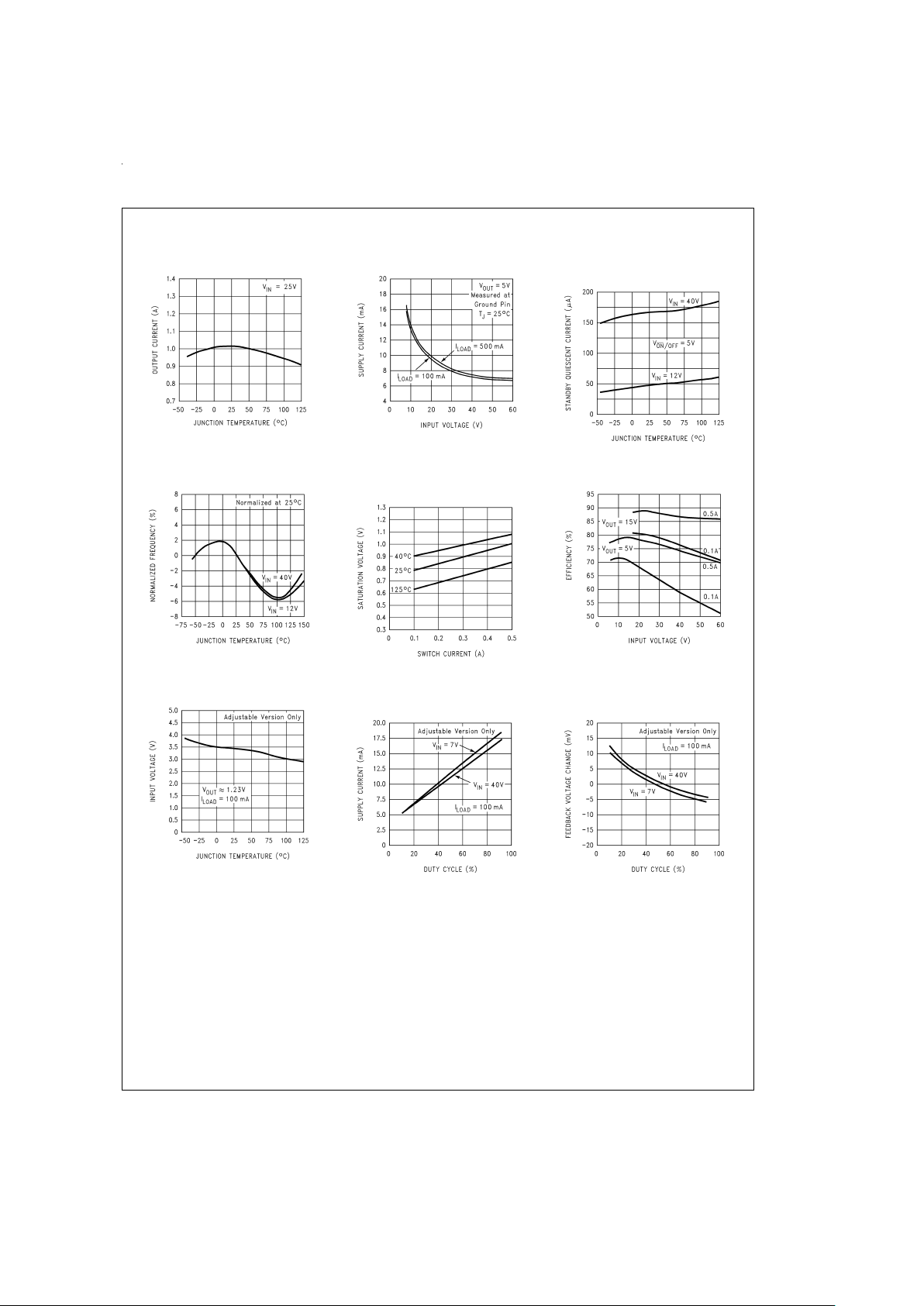
Typical Performance Characteristics (Circuit of
Figure 2
) (Continued)
Current Limit
DS011394-30
Supply Current
DS011394-31
Standby
Quiescent Current
DS011394-32
Oscillator Frequency
DS011394-33
Switch Saturation
Voltage
DS011394-34
Efficiency
DS011394-35
Minimum Operating Voltage
DS011394-36
Supply Current
vs Duty Cycle
DS011394-37
Feedback Voltage
vs Duty Cycle
DS011394-38
www.national.com7
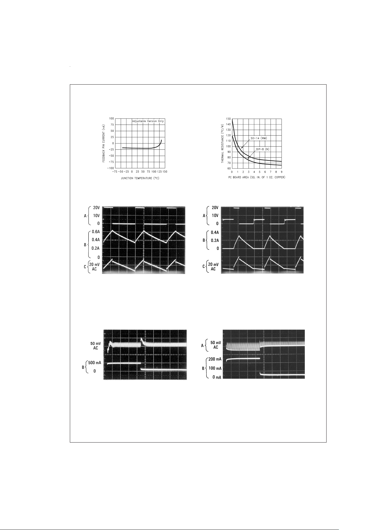
Typical Performance Characteristics (Circuit of
Figure 2
) (Continued)
Feedback
Pin Current
DS011394-39
Junction to Ambient
Thermal Resistance
DS011394-40
Continuous Mode Switching Waveforms
V
OUT
=
5V, 500 mA Load Current, L=330 µH
DS011394-6
Notes:
A: Output Pin Voltage, 10V/div
B: Inductor Current, 0.2 A/div
C: Output Ripple Voltage, 20 mV/div,
AC-Coupled
Horizontal Time Base: 5 µs/div
Discontinuous Mode Switching Waveforms
V
OUT
=
5V, 100 mA Load Current, L=100 µH
DS011394-7
Notes:
A: Output Pin Voltage, 10V/div
B: Inductor Current, 0.2 A/div
C: Output Ripple Voltage, 20 mV/div,
AC-Coupled
Horizontal Time Base: 5 µs/div
500 mA Load Transient Response for Continuous
Mode Operation. L=330 µH, C
OUT
=
300 µF
DS011394-8
Notes:
A: Output Voltage, 50 mV/div.
AC Coupled
B: 100 mA to 500 mA Load Pulse
Horizontal Time Base: 200 µs/div
250 mA Load Transient Response for Discontinuous
Mode Operation. L=68 µH, C
OUT
=
470 µF
DS011394-9
Notes:
A: Output Voltage, 50 mV/div.
AC Coupled
B: 50 mA to 250 mA Load Pulse
Horizontal Time Base: 200 µs/div
www.national.com 8
 Loading...