


 Loading...
Motorola MC68332GMFC16, MC68332GVFV16, MC68332GVFV20, MC68332MFC16, MC68332MFC20 Datasheet
...MOTOROLA
SEMICONDUCTOR
TECHNICAL DATA
Order this document by MC68332TS/D Rev. 2
MC68332
Technical Summary
32-Bit Modular Microcontroller
1 Introduction
The MC68332, a highly-integrated 32-bit microcontroller, combines high-performance data manipulation capabilities with powerful peripheral subsystems. The MCU is built up from standard modules that interface through a common intermodule bus (IMB). Standardization facilitates rapid development of devices tailored for specific applications.
The MCU incorporates a 32-bit CPU (CPU32), a system integration module (SIM), a time processor unit (TPU), a queued serial module (QSM), and a 2-Kbyte static RAM module with TPU emulation capability (TPURAM).
The MCU can either synthesize an internal clock signal from an external reference or use an external clock input directly. Operation with a 32.768-kHz reference frequency is standard. The maximum system clock speed is 20.97 MHz. System hardware and software allow changes in clock rate during operation. Because MCU operation is fully static, register and memory contents are not affected by clock rate changes.
High-density complementary metal-oxide semiconductor (HCMOS) architecture makes the basic power consumption of the MCU low. Power consumption can be minimized by stopping the system clock. The CPU32 instruction set includes a low-power stop (LPSTOP) command that efficiently implements this capability.
This document contains information on a new product. Specifications and information herein are subject to change without notice.
© MOTOROLA INC., 1993, 1996

Table 1 Ordering Information
Package Type |
TPU Type |
Temperature |
Frequency |
Package |
Order Number |
|
|
|
(MHz) |
Order |
|
|
|
|
|
Quantity |
|
|
|
|
|
|
|
132-Pin PQFP |
Motion Control |
–40 to +85 °C |
16 MHz |
2 pc tray |
SPAKMC332GCFC16 |
|
|
|
|
|
|
|
|
|
|
36 pc tray |
MC68332GCFC16 |
|
|
|
|
|
|
|
|
|
20 MHz |
2 pc tray |
SPAKMC332GCFC20 |
|
|
|
|
|
|
|
|
|
|
36 pc tray |
MC68332GCFC20 |
|
|
|
|
|
|
|
|
–40 to +105 °C |
16 MHz |
2 pc tray |
SPAKMC332GVFC16 |
|
|
|
|
|
|
|
|
|
|
36 pc tray |
MC68332GVFC16 |
|
|
|
|
|
|
|
|
|
20 MHz |
2 pc tray |
SPAKMC332GVFC20 |
|
|
|
|
|
|
|
|
|
|
36 pc tray |
MC68332GVFC20 |
|
|
|
|
|
|
|
|
–40 to +125 °C |
16 MHz |
2 pc tray |
SPAKMC332GMFC16 |
|
|
|
|
|
|
|
|
|
|
36 pc tray |
MC68332GMFC16 |
|
|
|
|
|
|
|
|
|
20 MHz |
2 pc tray |
SPAKMC332GMFC20 |
|
|
|
|
|
|
|
|
|
|
36 pc tray |
MC68332GMFC20 |
|
|
|
|
|
|
|
Standard |
–40 to +85 °C |
16 MHz |
2 pc tray |
SPAKMC332CFC16 |
|
|
|
|
|
|
|
|
|
|
36 pc tray |
MC68332CFC16 |
|
|
|
|
|
|
|
|
|
20 MHz |
2 pc tray |
SPAKMC332CFC20 |
|
|
|
|
|
|
|
|
|
|
36 pc tray |
MC68332CFC20 |
|
|
|
|
|
|
|
|
–40 to +105 °C |
16 MHz |
2 pc tray |
SPAKMC332VFC16 |
|
|
|
|
|
|
|
|
|
|
36 pc tray |
MC68332VFC16 |
|
|
|
|
|
|
|
|
|
20 MHz |
2 pc tray |
SPAKMC332VFC20 |
|
|
|
|
|
|
|
|
|
|
36 pc tray |
MC68332VFC20 |
|
|
|
|
|
|
|
|
–40 to +125 °C |
16 MHz |
2 pc tray |
SPAKMC332MFC16 |
|
|
|
|
|
|
|
|
|
|
36 pc tray |
MC68332MFC16 |
|
|
|
|
|
|
|
|
|
20 MHz |
2 pc tray |
SPAKMC332MFC20 |
|
|
|
|
|
|
|
|
|
|
36 pc tray |
MC68332MFC20 |
|
|
|
|
|
|
|
Std w/enhanced |
–40 to +85 °C |
16 MHz |
2 pc tray |
SPAKMC332ACFC16 |
|
PPWA |
|
|
|
|
|
|
|
36 pc tray |
MC68332ACFC16 |
|
|
|
|
|
||
|
|
|
|
|
|
|
|
|
20 MHz |
2 pc tray |
SPAKMC332ACFC20 |
|
|
|
|
|
|
|
|
|
|
36 pc tray |
MC68332ACFC20 |
|
|
|
|
|
|
|
|
–40 to +105 °C |
16 MHz |
2 pc tray |
SPAKMC332AVFC16 |
|
|
|
|
|
|
|
|
|
|
36 pc tray |
MC68332AVFC16 |
|
|
|
|
|
|
|
|
|
20 MHz |
2 pc tray |
SPAKMC332AVFC20 |
|
|
|
|
|
|
|
|
|
|
36 pc tray |
MC68332AVFC20 |
|
|
|
|
|
|
|
|
–40 to +125 °C |
16 MHz |
2 pc tray |
SPAKMC332AMFC16 |
|
|
|
|
|
|
|
|
|
|
36 pc tray |
MC68332AMFC16 |
|
|
|
|
|
|
|
|
|
20 MHz |
2 pc tray |
SPAKMC332AMFC20 |
|
|
|
|
|
|
|
|
|
|
36 pc tray |
MC68332AMFC20 |
|
|
|
|
|
|
MOTOROLA |
MC68332 |
2 |
MC68332TS/D |

Table 1 Ordering Information (Continued)
Package Type |
TPU Type |
Temperature |
Frequency |
Package |
Order Number |
|
|
|
(MHz) |
Order |
|
|
|
|
|
Quantity |
|
|
|
|
|
|
|
144-Pin QFP |
Motion Control |
–40 to +85 °C |
16 MHz |
2 pc tray |
SPAKMC332GCFV16 |
|
|
|
|
|
|
|
|
|
|
44 pc tray |
MC68332GCFVV16 |
|
|
|
|
|
|
|
|
|
20 MHz |
2 pc tray |
SPAKMC332GCFV20 |
|
|
|
|
|
|
|
|
|
|
44 pc tray |
MC68332GCFV20 |
|
|
|
|
|
|
|
|
–40 to +105 °C |
16 MHz |
2 pc tray |
SPAKMC332GVFV16 |
|
|
|
|
|
|
|
|
|
|
44 pc tray |
MC68332GVFV16 |
|
|
|
|
|
|
|
|
|
20 MHz |
2 pc tray |
SPAKMC332GVFV20 |
|
|
|
|
|
|
|
|
|
|
44 pc tray |
MC68332GVFV20 |
|
|
|
|
|
|
|
|
–40 to +125 °C |
16 MHz |
2 pc tray |
SPAKMC332GMFV16 |
|
|
|
|
|
|
|
|
|
|
44 pc tray |
MC68332GMFV16 |
|
|
|
|
|
|
|
|
|
20 MHz |
2 pc tray |
SPAKMC332GMFV20 |
|
|
|
|
|
|
|
|
|
|
44 pc tray |
MC68332GMFVV20 |
|
|
|
|
|
|
|
Standard |
–40 to +85 °C |
16 MHz |
2 pc tray |
SPAKMC332CFV16 |
|
|
|
|
|
|
|
|
|
|
44 pc tray |
MC68332CFV16 |
|
|
|
|
|
|
|
|
|
20 MHz |
2 pc tray |
SPAKMC332CFVV20 |
|
|
|
|
|
|
|
|
|
|
44 pc tray |
MC68332CFV20 |
|
|
|
|
|
|
|
|
–40 to +105 °C |
16 MHz |
2 pc tray |
SPAKMC332VFV16 |
|
|
|
|
|
|
|
|
|
|
44 pc tray |
MC68332VFV16 |
|
|
|
|
|
|
|
|
|
20 MHz |
2 pc tray |
SPAKMC332VFV20 |
|
|
|
|
|
|
|
|
|
|
44 pc tray |
MC68332VFV20 |
|
|
|
|
|
|
|
|
–40 to +125 °C |
16 MHz |
2 pc tray |
SPAKMC332MFV16 |
|
|
|
|
|
|
|
|
|
|
44 pc tray |
MC68332MFV16 |
|
|
|
|
|
|
|
|
|
20 MHz |
2 pc tray |
SPAKMC332MFV20 |
|
|
|
|
|
|
|
|
|
|
44 pc tray |
MC68332MFV20 |
|
|
|
|
|
|
|
Std w/enhanced |
–40 to +85 °C |
16 MHz |
2 pc tray |
SPAKMC332ACFV16 |
|
PPWA |
|
|
|
|
|
|
|
44 pc tray |
MC68332ACFV16 |
|
|
|
|
|
||
|
|
|
|
|
|
|
|
|
20 MHz |
2 pc tray |
SPAKMC332ACFV20 |
|
|
|
|
|
|
|
|
|
|
44 pc tray |
MC68332ACFV20 |
|
|
|
|
|
|
|
|
–40 to +105 °C |
16 MHz |
2 pc tray |
SPAKMC332AVFV16 |
|
|
|
|
|
|
|
|
|
|
44 pc tray |
MC68332AVFV16 |
|
|
|
|
|
|
|
|
|
20 MHz |
2 pc tray |
SPAKMC332AVFC20 |
|
|
|
|
|
|
|
|
|
|
44 pc tray |
MC68332AVFV20 |
|
|
|
|
|
|
|
|
–40 to +125 °C |
16 MHz |
2 pc tray |
SPAKMC332AMFV16 |
|
|
|
|
|
|
|
|
|
|
44 pc tray |
MC68332AMFV16 |
|
|
|
|
|
|
|
|
|
20 MHz |
2 pc tray |
SPAKMC332AMFV20 |
|
|
|
|
|
|
|
|
|
|
44 pc tray |
MC68332AMFV20 |
|
|
|
|
|
|
MC68332 |
MOTOROLA |
MC68332TS/D |
3 |

|
TABLE OF CONTENTS |
|
Section |
|
Page |
1 |
Introduction |
1 |
1.1 |
Features ...................................................................................................................................... |
5 |
1.2 |
Block Diagram ............................................................................................................................. |
6 |
1.3 |
Pin Assignments .......................................................................................................................... |
7 |
1.4 |
Address Map ............................................................................................................................... |
9 |
1.5 |
Intermodule Bus .......................................................................................................................... |
9 |
2 |
Signal Descriptions |
10 |
2.1 |
Pin Characteristics .................................................................................................................... |
10 |
2.2 |
MCU Power Connections .......................................................................................................... |
11 |
2.3 |
MCU Driver Types ..................................................................................................................... |
11 |
2.4 |
Signal Characteristics ................................................................................................................ |
12 |
2.5 |
Signal Function .......................................................................................................................... |
13 |
3 |
System Integration Module |
15 |
3.1 |
Overview ................................................................................................................................... |
15 |
3.2 |
System Configuration and Protection ........................................................................................ |
17 |
3.3 |
System Clock ............................................................................................................................ |
23 |
3.4 |
External Bus Interface ............................................................................................................... |
26 |
3.5 |
Chip Selects .............................................................................................................................. |
29 |
3.6 |
General-Purpose Input/Output .................................................................................................. |
36 |
3.7 |
Resets ....................................................................................................................................... |
38 |
3.8 |
Interrupts ................................................................................................................................... |
41 |
3.9 |
Factory Test Block ..................................................................................................................... |
43 |
4 |
Central Processor Unit |
44 |
4.1 |
Overview ................................................................................................................................... |
44 |
4.2 |
Programming Model .................................................................................................................. |
44 |
4.3 |
Status Register .......................................................................................................................... |
46 |
4.4 |
Data Types ................................................................................................................................ |
46 |
4.5 |
Addressing Modes ..................................................................................................................... |
46 |
4.6 |
Instruction Set Summary ........................................................................................................... |
47 |
4.7 |
Background Debugging Mode ................................................................................................... |
51 |
5 |
Time Processor Unit |
52 |
5.1 |
MC68332 and MC68332A Time Functions ............................................................................... |
52 |
5.2 |
MC68332G Time Functions ...................................................................................................... |
55 |
5.3 |
Programmer's Model ................................................................................................................. |
57 |
5.4 |
Parameter RAM ......................................................................................................................... |
58 |
5.5 |
TPU Registers ........................................................................................................................... |
58 |
6 |
Queued Serial Module |
64 |
6.1 |
Overview ................................................................................................................................... |
64 |
6.2 |
Address Map ............................................................................................................................. |
65 |
6.3 |
Pin Function .............................................................................................................................. |
66 |
6.4 |
QSM Registers .......................................................................................................................... |
66 |
6.5 |
QSPI Submodule ....................................................................................................................... |
71 |
6.6 |
SCI Submodule ......................................................................................................................... |
79 |
7 |
Standby RAM with TPU Emulation RAM |
84 |
7.1 |
Overview ................................................................................................................................... |
84 |
7.2 |
TPURAM Register Block ........................................................................................................... |
84 |
7.3 |
TPURAM Registers ................................................................................................................... |
84 |
7.4 |
TPURAM Operation .................................................................................................................. |
85 |
8 |
Summary of Changes |
86 |
MOTOROLA |
MC68332 |
4 |
MC68332TS/D |

1.1Features
•Central Processing Unit (CPU32)
—32-Bit Architecture
—Virtual Memory Implementation
—Table Lookup and Interpolate Instruction
—Improved Exception Handling for Controller Applications
—High-Level Language Support
—Background Debugging Mode
—Fully Static Operation
•System Integration Module (SIM)
—External Bus Support
—Programmable Chip-Select Outputs
—System Protection Logic
—Watchdog Timer, Clock Monitor, and Bus Monitor
—Two 8-Bit Dual Function Input/Output Ports
—One 7-Bit Dual Function Output Port
—Phase-Locked Loop (PLL) Clock System
•Time Processor Unit (TPU)
—Dedicated Microengine Operating Independently of CPU32
—16 Independent, Programmable Channels and Pins
—Any Channel can Perform any Time Function
—Two Timer Count Registers with Programmable Prescalers
—Selectable Channel Priority Levels
•Queued Serial Module (QSM)
—Enhanced Serial Communication Interface
—Queued Serial Peripheral Interface
—One 8-Bit Dual Function Port
•Static RAM Module with TPU Emulation Capability (TPURAM)
—2-Kbytes of Static RAM
—May be Used as Normal RAM or TPU Microcode Emulation RAM
MC68332 |
MOTOROLA |
MC68332TS/D |
5 |

1.2 Block Diagram
VSTBY
TPUCH[15:0] |
TPUCH[15:0] |
|
T2CLK |
T2CLK |
2 KBYTES |
|
TPU |
RAM |
|
|
CHIP |
|
|
CSBOOT |
|
SELECTS BR |
|
|
||
|
|
ADDR23/CS10 |
||
BG |
|
|
PC6/ADDR22/CS9 |
|
BGACK |
|
C |
PC5/ADDR21/CS8 |
|
CS[10:0] |
CONTROL |
PC4/ADDR20/CS7 |
||
PORT |
||||
|
PC3/ADDR19/CS6 |
|||
FC2 |
PC2/FC2/CS5 |
|||
FC1 |
PC1/FC1/CS4 |
|||
FC0 |
PC0/FC0/CS3 |
|||
|
|
|||
|
|
|
BGACK/CS2 |
|
|
|
|
BG/CS1 |
|
|
ADDR[23:19] |
|
BR/CS0 |
|
|
|
|
||
ADDR[23:0] |
|
|
ADDR[18:0] |
IMB
SIZ1
SIZ0
EBI DS  AS
AS 
RMC
AVEC  DSACK1
  DSACK0
CONTROL |
PORT E |
 PE7/SIZ1
 PE6/SIZ0
 PE5/DS
 PE4/AS
 PE3/RMC
 PE2/AVEC
 PE1/DSACK1
  PE0/DSACK0
RXD |
|
|
|
|
PQS7/TXD |
|
|
TXD |
|
PQS6/PCS3 |
|
|
PCS3 |
|
QS5/PCS2 |
PORTQS |
CONTROL |
PCS2 |
|
PQS4/PCS1 |
PCS1 |
|
||
|
|
|
||
PQS3/PCS0/SS |
|
|
PCS0/SS |
|
PQS2/SCK |
|
|
SCK |
|
PQS1/MOSI |
|
|
MOSI |
|
PQS0/MISO |
|
|
MISO |
|
|
|
|
QSM |
CPU 32 |
|
BKPT IFETCH |
IPIPE |
DSI |
DSO |
DSCLK |
BKPT/DSCLK |
|
|
|
|
|
IFETCH/DSI |
CONTROL |
|
|
|
|
IPIPE/DSO |
|
|
|
|
|
|
|
|
|
|
DATA[15:0] 
 DATA[15:0]
|
R/W |
|
|
RESET |
|
|
HALT |
|
|
BERR |
|
IRQ[7:1] |
PF7/IRQ7 |
|
|
PF6/IRQ6 |
|
CONTROL PORTF |
PF5/IRQ5 |
|
PF2/IRQ2 |
||
|
PF4/IRQ4 |
|
|
PF3/IRQ3 |
|
|
PF1/IRQ1 |
|
MODCLK |
PF0/MODCLK |
|
|
CLKOUT |
|
CLOCK |
XTAL |
|
EXTAL |
||
|
||
FREEZE |
XFC |
|
VDDSYN |
||
|
TSC |
CONTROL |
TSC |
TEST |
|
|
|
|
|
QUOT |
|
FREEZE/QUOT |
|
|
332 BLOCK |
Figure 1 MCU Block Diagram
MOTOROLA |
MC68332 |
6 |
MC68332TS/D |
1.3 Pin Assignments
|
|
|
|
|
V |
TPUCH0 |
|
TPUCH1 |
|
TPUCH2 |
|
TPUCH3 |
|
TPUCH4 |
|
TPUCH5 |
|
TPUCH6 |
|
TPUCH7 |
V |
V |
TPUCH8 |
|
TPUCH9 |
TPUCH10 |
|
TPUCH11 |
V |
V |
TPUCH12 |
TPUCH13 |
|
TPUCH14 |
|
TPUCH15 |
|
T2CLK |
V |
V |
|
ADDR23/CS10 |
|
PC6/ADDR22/CS9 |
|
PC5/ADDR21/CS8 |
|
PC4/ADDR20/CS7 |
|
PC3/ADDR19/CS6 |
|
PC2/FC2/CS5 |
|
PC1/FC1/CS4 |
|
PC0/FC0/CS3 |
V |
|||||||||||||||||||
|
|
|
|
|
|
|
|
|
|
|
|
|
|
|
|
|
|
|
|
|
|
|
|
|
||||||||||||||||||||||||||||||||||||||||||||||||||||
|
|
|
|
|
|
|
|
|
|
|
|
|
|
|
|
|
|
|
|
|
|
|
|
|
||||||||||||||||||||||||||||||||||||||||||||||||||||
|
|
|
|
|
|
SS |
|
|
|
|
|
|
|
|
|
|
|
|
|
|
|
|
|
SS |
|
DD |
|
|
|
|
|
|
|
|
|
SS |
|
DD |
|
|
|
|
|
|
|
|
|
|
SS |
DD |
|
|
|
|
|
|
|
|
|
|
|
|
|
|
|
|
|
SS |
||||||||
|
|
|
|
|
|
|
|
|
|
|
|
|
|
|
|
|
|
|
|
|
|
|
|
|
|
|
|
|
|
|
|
|
|
|
|
|
|
|
|
|
|
|
|
|
|
|
|
|
|
|
|
|
|
|
|
|
|
|
|
|
|
|
|
|
|
|
|
|
|
|
|
|
|
|
|
|
|
|
|
|
|
|
|
|
|
|
|
|
|
|
|
|
|
|
|
|
|
|
|
|
|
|
|
|
|
|
|
|
|
|
|
|
|
|
|
|
|
|
|
|
|
|
|
|
|
|
|
|
|
|
|
|
|
|
|
|
|
|
|
|
|
|
|
|
|
|
|
|
|
|
|
|
|
|
|
|
|
|
|
|
|
|
|
|
|
|
|
|
|
|
|
|
|
|
|
|
|
|
|
|
|
|
|
|
|
|
|
|
|
|
|
|
|
|
|
|
|
|
|
|
|
|
|
|
|
|
|
|
|
|
|
|
|
|
|
|
|
|
|
|
|
|
|
|
|
|
|
|
|
|
VDD |
|
|
17 |
|
16 |
15 |
14 |
13 |
12 |
11 |
10 |
9 |
|
8 |
|
7 |
|
6 |
5 |
|
4 |
3 |
|
2 |
|
1 |
|
132 |
|
131 |
130 |
129 |
128 |
127 |
|
126 |
|
125 |
124 |
123 |
122 |
121 |
120 |
119 |
118 |
117 |
|
|||||||||||||||||||||||||||||
|
18 |
|
|
|
|
|
|
|
|
|
|
|
|
|
|
|
|
|
|
|
|
|
|
|
|
|
|
|
|
|
|
|
|
|
|
|
|
|
|
|
|
|
|
|
|
|
|
|
|
|
|
|
|
|
|
|
|
|
|
|
|
|
|
|
|
|
|
|
|
116 |
||||||
|
|
|
|
|
|
|
|
|
|
|
|
|
|
|
|
|
|
|
|
|
|
|
|
|
|
|
|
|
|
|
|
|
|
|
|
|
|
|
|
|
|
|
|
|
|
|
|
|
|
|
|
|
|
|
|
|
|
|
|
|
|
|
|
|
|
|
|
|
|
|||||||
|
|
|
|
|
|
|
|
|
|
|
|
|
|
|
|
|
|
|
|
|
|
|
|
|
|
|
|
|
|
|
|
|
|
|
|
|
|
|
|
|
|
|
|
|
|
|
|
|
|
|
|
|
|
|
|
|
|
|
|
|
|
|
|
|
|
|
|
|
||||||||
VSTBY |
|
19 |
|
|
|
|
|
|
|
|
|
|
|
|
|
|
|
|
|
|
|
|
|
|
|
|
|
|
|
|
|
|
|
|
|
|
|
|
|
|
|
|
|
|
|
|
|
|
|
|
|
|
|
|
|
|
|
|
|
|
|
|
|
|
|
|
|
|
|
|
115 |
|||||
|
|
|
|
|
|
|
|
|
|
|
|
|
|
|
|
|
|
|
|
|
|
|
|
|
|
|
|
|
|
|
|
|
|
|
|
|
|
|
|
|
|
|
|
|
|
|
|
|
|
|
|
|
|
|
|
|
|
|
|
|
|
|
|
|
|
|
|
|
|
|||||||
|
|
|
|
|
|
|
|
|
|
|
|
|
|
|
|
|
|
|
|
|
|
|
|
|
|
|
|
|
|
|
|
|
|
|
|
|
|
|
|
|
|
|
|
|
|
|
|
|
|
|
|
|
|
|
|
|
|
|
|
|
|
|
|
|
|
|
|
|
|
|||||||
ADDR1 |
|
20 |
|
|
|
|
|
|
|
|
|
|
|
|
|
|
|
|
|
|
|
|
|
|
|
|
|
|
|
|
|
|
|
|
|
|
|
|
|
|
|
|
|
|
|
|
|
|
|
|
|
|
|
|
|
|
|
|
|
|
|
|
|
|
|
|
|
|
|
|
114 |
|||||
|
|
|
|
|
|
|
|
|
|
|
|
|
|
|
|
|
|
|
|
|
|
|
|
|
|
|
|
|
|
|
|
|
|
|
|
|
|
|
|
|
|
|
|
|
|
|
|
|
|
|
|
|
|
|
|
|
|
|
|
|
|
|
|
|
|
|
|
|
|
|||||||
ADDR2 |
|
|
21 |
|
|
|
|
|
|
|
|
|
|
|
|
|
|
|
|
|
|
|
|
|
|
|
|
|
|
|
|
|
|
|
|
|
|
|
|
|
|
|
|
|
|
|
|
|
|
|
|
|
|
|
|
|
|
|
|
|
|
|
|
|
|
|
|
|
|
|
|
113 |
||||
|
|
|
|
|
|
|
|
|
|
|
|
|
|
|
|
|
|
|
|
|
|
|
|
|
|
|
|
|
|
|
|
|
|
|
|
|
|
|
|
|
|
|
|
|
|
|
|
|
|
|
|
|
|
|
|
|
|
|
|
|
|
|
|
|
|
|
|
|
|
|||||||
|
|
|
|
|
|
|
|
|
|
|
|
|
|
|
|
|
|
|
|
|
|
|
|
|
|
|
|
|
|
|
|
|
|
|
|
|
|
|
|
|
|
|
|
|
|
|
|
|
|
|
|
|
|
|
|
|
|
|
|
|
|
|
|
|
|
|
|
|
|
|||||||
ADDR3 |
|
22 |
|
|
|
|
|
|
|
|
|
|
|
|
|
|
|
|
|
|
|
|
|
|
|
|
|
|
|
|
|
|
|
|
|
|
|
|
|
|
|
|
|
|
|
|
|
|
|
|
|
|
|
|
|
|
|
|
|
|
|
|
|
|
|
|
|
|
|
|
112 |
|||||
|
|
|
|
|
|
|
|
|
|
|
|
|
|
|
|
|
|
|
|
|
|
|
|
|
|
|
|
|
|
|
|
|
|
|
|
|
|
|
|
|
|
|
|
|
|
|
|
|
|
|
|
|
|
|
|
|
|
|
|
|
|
|
|
|
|
|
|
|
|
|||||||
ADDR4 |
|
|
23 |
|
|
|
|
|
|
|
|
|
|
|
|
|
|
|
|
|
|
|
|
|
|
|
|
|
|
|
|
|
|
|
|
|
|
|
|
|
|
|
|
|
|
|
|
|
|
|
|
|
|
|
|
|
|
|
|
|
|
|
|
|
|
|
|
|
|
|
|
111 |
||||
|
|
|
|
|
|
|
|
|
|
|
|
|
|
|
|
|
|
|
|
|
|
|
|
|
|
|
|
|
|
|
|
|
|
|
|
|
|
|
|
|
|
|
|
|
|
|
|
|
|
|
|
|
|
|
|
|
|
|
|
|
|
|
|
|
|
|
|
|
|
|||||||
|
|
|
|
|
|
|
|
|
|
|
|
|
|
|
|
|
|
|
|
|
|
|
|
|
|
|
|
|
|
|
|
|
|
|
|
|
|
|
|
|
|
|
|
|
|
|
|
|
|
|
|
|
|
|
|
|
|
|
|
|
|
|
|
|
|
|
|
|
|
|||||||
ADDR5 |
|
24 |
|
|
|
|
|
|
|
|
|
|
|
|
|
|
|
|
|
|
|
|
|
|
|
|
|
|
|
|
|
|
|
|
|
|
|
|
|
|
|
|
|
|
|
|
|
|
|
|
|
|
|
|
|
|
|
|
|
|
|
|
|
|
|
|
|
|
|
|
110 |
|||||
|
|
|
|
|
|
|
|
|
|
|
|
|
|
|
|
|
|
|
|
|
|
|
|
|
|
|
|
|
|
|
|
|
|
|
|
|
|
|
|
|
|
|
|
|
|
|
|
|
|
|
|
|
|
|
|
|
|
|
|
|
|
|
|
|
|
|
|
|
|
|||||||
ADDR6 |
|
|
25 |
|
|
|
|
|
|
|
|
|
|
|
|
|
|
|
|
|
|
|
|
|
|
|
|
|
|
|
|
|
|
|
|
|
|
|
|
|
|
|
|
|
|
|
|
|
|
|
|
|
|
|
|
|
|
|
|
|
|
|
|
|
|
|
|
|
|
|
|
109 |
||||
|
|
|
|
|
|
|
|
|
|
|
|
|
|
|
|
|
|
|
|
|
|
|
|
|
|
|
|
|
|
|
|
|
|
|
|
|
|
|
|
|
|
|
|
|
|
|
|
|
|
|
|
|
|
|
|
|
|
|
|
|
|
|
|
|
|
|
|
|
|
|||||||
|
|
|
|
|
|
|
|
|
|
|
|
|
|
|
|
|
|
|
|
|
|
|
|
|
|
|
|
|
|
|
|
|
|
|
|
|
|
|
|
|
|
|
|
|
|
|
|
|
|
|
|
|
|
|
|
|
|
|
|
|
|
|
|
|
|
|
|
|
|
|||||||
ADDR7 |
|
26 |
|
|
|
|
|
|
|
|
|
|
|
|
|
|
|
|
|
|
|
|
|
|
|
|
|
|
|
|
|
|
|
|
|
|
|
|
|
|
|
|
|
|
|
|
|
|
|
|
|
|
|
|
|
|
|
|
|
|
|
|
|
|
|
|
|
|
|
|
108 |
|||||
|
|
|
|
|
|
|
|
|
|
|
|
|
|
|
|
|
|
|
|
|
|
|
|
|
|
|
|
|
|
|
|
|
|
|
|
|
|
|
|
|
|
|
|
|
|
|
|
|
|
|
|
|
|
|
|
|
|
|
|
|
|
|
|
|
|
|
|
|
|
|||||||
ADDR8 |
|
|
27 |
|
|
|
|
|
|
|
|
|
|
|
|
|
|
|
|
|
|
|
|
|
|
|
|
|
|
|
|
|
|
|
|
|
|
|
|
|
|
|
|
|
|
|
|
|
|
|
|
|
|
|
|
|
|
|
|
|
|
|
|
|
|
|
|
|
|
|
|
107 |
||||
|
|
|
|
|
|
|
|
|
|
|
|
|
|
|
|
|
|
|
|
|
|
|
|
|
|
|
|
|
|
|
|
|
|
|
|
|
|
|
|
|
|
|
|
|
|
|
|
|
|
|
|
|
|
|
|
|
|
|
|
|
|
|
|
|
|
|
|
|
|
|||||||
|
|
|
|
|
|
|
|
|
|
|
|
|
|
|
|
|
|
|
|
|
|
|
|
|
|
|
|
|
|
|
|
|
|
|
|
|
|
|
|
|
|
|
|
|
|
|
|
|
|
|
|
|
|
|
|
|
|
|
|
|
|
|
|
|
|
|
|
|
|
|||||||
VDD |
|
28 |
|
|
|
|
|
|
|
|
|
|
|
|
|
|
|
|
|
|
|
|
|
|
|
|
|
|
|
|
|
|
|
|
|
|
|
|
|
|
|
|
|
|
|
|
|
|
|
|
|
|
|
|
|
|
|
|
|
|
|
|
|
|
|
|
|
|
|
|
106 |
|||||
|
|
|
|
|
|
|
|
|
|
|
|
|
|
|
|
|
|
|
|
|
|
|
|
|
|
|
|
|
|
|
|
|
|
|
|
|
|
|
|
|
|
|
|
|
|
|
|
|
|
|
|
|
|
|
|
|
|
|
|
|
|
|
|
|
|
|
|
|
|
|||||||
|
|
|
|
|
|
|
|
|
|
|
|
|
|
|
|
|
|
|
|
|
|
|
|
|
|
|
|
|
|
|
|
|
|
|
|
|
|
|
|
|
|
|
|
|
|
|
|
|
|
|
|
|
|
|
|
|
|
|
|
|
|
|
|
|
|
|
|
|
||||||||
VSS |
|
29 |
|
|
|
|
|
|
|
|
|
|
|
|
|
|
|
|
|
|
|
|
|
|
|
|
|
|
|
|
|
|
|
|
|
|
|
|
|
|
|
|
|
|
|
|
|
|
|
|
|
|
|
|
|
|
|
|
|
|
|
|
|
|
|
|
|
|
|
|
105 |
|||||
|
|
|
|
|
|
|
|
|
|
|
|
|
|
|
|
|
|
|
|
|
|
|
|
|
|
|
|
|
|
|
|
|
|
|
|
|
|
|
|
|
|
|
|
|
|
|
|
|
|
|
|
|
|
|
|
|
|
|
|
|
|
|
|
|
|
|
|
|
|
|||||||
|
|
|
|
|
|
|
|
|
|
|
|
|
|
|
|
|
|
|
|
|
|
|
|
|
|
|
|
|
|
|
|
|
|
|
|
|
|
|
|
|
|
|
|
|
|
|
|
|
|
|
|
|
|
|
|
|
|
|
|
|
|
|
|
|
|
|
|
|
|
|||||||
ADDR9 |
|
30 |
|
|
|
|
|
|
|
|
|
|
|
|
|
|
|
|
|
|
|
|
|
|
|
|
|
|
|
|
|
|
|
|
|
|
|
|
|
|
|
|
|
|
|
|
|
|
|
|
|
|
|
|
|
|
|
|
|
|
|
|
|
|
|
|
|
|
|
|
104 |
|||||
|
|
|
|
|
|
|
|
|
|
|
|
|
|
|
|
|
|
|
|
|
|
|
|
|
|
|
|
|
|
|
|
|
|
|
|
|
|
|
|
|
|
|
|
|
|
|
|
|
|
|
|
|
|
|
|
|
|
|
|
|
|
|
|
|
|
|
|
|
|
|||||||
ADDR10 |
|
|
31 |
|
|
|
|
|
|
|
|
|
|
|
|
|
|
|
|
|
|
|
|
|
|
|
|
|
|
|
|
|
|
|
|
|
|
|
|
|
|
|
|
|
|
|
|
|
|
|
|
|
|
|
|
|
|
|
|
|
|
|
|
|
|
|
|
|
|
|
|
103 |
||||
|
|
|
|
|
|
|
|
|
|
|
|
|
|
|
|
|
|
|
|
|
|
|
|
|
|
|
|
|
|
|
|
|
|
|
|
|
|
|
|
|
|
|
|
|
|
|
|
|
|
|
|
|
|
|
|
|
|
|
|
|
|
|
|
|
|
|
|
|
|
|||||||
|
|
|
|
|
|
|
|
|
|
|
|
|
|
|
|
|
|
|
|
|
|
|
|
|
|
|
|
|
|
|
|
|
|
|
|
|
|
|
|
|
|
|
|
|
|
|
|
|
|
|
|
|
|
|
|
|
|
|
|
|
|
|
|
|
|
|
|
|
|
|||||||
ADDR11 |
|
32 |
|
|
|
|
|
|
|
|
|
|
|
|
|
|
|
|
|
|
|
|
|
|
|
|
|
|
|
|
|
|
|
|
|
|
|
|
|
|
|
|
|
|
|
|
|
|
|
|
|
|
|
|
|
|
|
|
|
|
|
|
|
|
|
|
|
|
|
|
102 |
|||||
|
|
|
|
|
|
|
|
|
|
|
|
|
|
|
|
|
|
|
|
|
|
|
|
|
|
|
|
|
|
|
|
|
|
|
|
|
|
|
|
|
|
|
|
|
|
|
|
|
|
|
|
|
|
|
|
|
|
|
|
|
|
|
|
|
|
|
|
|
|
|||||||
ADDR12 |
|
|
33 |
|
|
|
|
|
|
|
|
|
|
|
|
|
|
|
|
|
|
|
|
|
|
|
|
|
|
|
|
|
|
|
|
|
|
|
|
|
|
|
|
|
|
|
|
|
|
|
|
|
|
|
|
|
|
|
|
|
|
|
|
|
|
|
|
|
|
|
|
101 |
||||
|
|
|
|
|
|
|
|
|
|
|
|
|
|
|
|
|
|
|
|
|
|
|
|
|
|
|
|
|
|
|
|
|
|
|
|
|
|
|
|
|
|
|
|
|
|
|
|
|
|
|
|
|
|
|
|
|
|
|
|
|
|
|
|
|
|
|
|
|
|
|||||||
|
|
|
|
|
|
|
|
|
|
|
|
|
|
|
|
|
|
|
|
|
|
|
|
|
|
|
|
|
|
|
|
|
|
|
|
|
|
|
|
|
|
|
|
|
|
|
|
|
|
|
|
|
|
|
|
|
|
|
|
|
|
|
|
|
|
|
|
|
|
|||||||
VSS |
|
34 |
|
|
|
|
|
|
|
|
|
|
|
|
|
|
|
|
|
|
|
|
|
|
|
|
|
|
|
|
|
|
|
|
MC68332 |
|
|
|
|
|
|
|
|
|
|
|
|
|
|
|
|
|
|
|
|
|
|
|
|
|
|
|
|
100 |
||||||||||||
|
|
|
|
|
|
|
|
|
|
|
|
|
|
|
|
|
|
|
|
|
|
|
|
|
|
|
|
|
|
|
|
|
|
|
|
|
|
|
|
|
|
|
|
|
|
|
|
|
|
|
|
|
|
|
|
|
|
|
|
|
|
|||||||||||||||
|
|
|
|
|
|
|
|
|
|
|
|
|
|
|
|
|
|
|
|
|
|
|
|
|
|
|
|
|
|
|
|
|
|
|
|
|
|
|
|
|
|
|
|
|
|
|
|
|
|
|
|
|
|
|
|
|
|
|
|
|
||||||||||||||||
ADDR13 |
|
|
35 |
|
|
|
|
|
|
|
|
|
|
|
|
|
|
|
|
|
|
|
|
|
|
|
|
|
|
|
|
|
|
|
|
|
|
|
|
|
|
|
|
|
|
|
|
|
|
|
|
|
|
|
|
|
|
|
|
|
|
|
|
|
|
|
|
|
|
|
|
99 |
||||
|
|
|
|
|
|
|
|
|
|
|
|
|
|
|
|
|
|
|
|
|
|
|
|
|
|
|
|
|
|
|
|
|
|
|
|
|
|
|
|
|
|
|
|
|
|
|
|
|
|
|
|
|
|
|
|
|
|
|
|
|
|
|
|
|
|
|
|
|
|
|||||||
ADDR14 |
|
36 |
|
|
|
|
|
|
|
|
|
|
|
|
|
|
|
|
|
|
|
|
|
|
|
|
|
|
|
|
|
|
|
|
|
|
|
|
|
|
|
|
|
|
|
|
|
|
|
|
|
|
|
|
|
|
|
|
|
|
|
|
|
|
|
|
|
|
|
|
98 |
|||||
|
|
|
|
|
|
|
|
|
|
|
|
|
|
|
|
|
|
|
|
|
|
|
|
|
|
|
|
|
|
|
|
|
|
|
|
|
|
|
|
|
|
|
|
|
|
|
|
|
|
|
|
|
|
|
|
|
|
|
|
|
|
|
|
|
|
|
|
|
|
|||||||
ADDR15 |
|
|
37 |
|
|
|
|
|
|
|
|
|
|
|
|
|
|
|
|
|
|
|
|
|
|
|
|
|
|
|
|
|
|
|
|
|
|
|
|
|
|
|
|
|
|
|
|
|
|
|
|
|
|
|
|
|
|
|
|
|
|
|
|
|
|
|
|
|
|
|
|
97 |
||||
|
|
|
|
|
|
|
|
|
|
|
|
|
|
|
|
|
|
|
|
|
|
|
|
|
|
|
|
|
|
|
|
|
|
|
|
|
|
|
|
|
|
|
|
|
|
|
|
|
|
|
|
|
|
|
|
|
|
|
|
|
|
|
|
|
|
|
|
|
|
|||||||
|
|
|
|
|
|
|
|
|
|
|
|
|
|
|
|
|
|
|
|
|
|
|
|
|
|
|
|
|
|
|
|
|
|
|
|
|
|
|
|
|
|
|
|
|
|
|
|
|
|
|
|
|
|
|
|
|
|
|
|
|
|
|
|
|
|
|
|
|
|
|||||||
ADDR16 |
|
38 |
|
|
|
|
|
|
|
|
|
|
|
|
|
|
|
|
|
|
|
|
|
|
|
|
|
|
|
|
|
|
|
|
|
|
|
|
|
|
|
|
|
|
|
|
|
|
|
|
|
|
|
|
|
|
|
|
|
|
|
|
|
|
|
|
|
|
|
|
96 |
|||||
|
|
|
|
|
|
|
|
|
|
|
|
|
|
|
|
|
|
|
|
|
|
|
|
|
|
|
|
|
|
|
|
|
|
|
|
|
|
|
|
|
|
|
|
|
|
|
|
|
|
|
|
|
|
|
|
|
|
|
|
|
|
|
|
|
|
|
|
|
|
|||||||
VDD |
|
|
39 |
|
|
|
|
|
|
|
|
|
|
|
|
|
|
|
|
|
|
|
|
|
|
|
|
|
|
|
|
|
|
|
|
|
|
|
|
|
|
|
|
|
|
|
|
|
|
|
|
|
|
|
|
|
|
|
|
|
|
|
|
|
|
|
|
|
|
|
|
95 |
||||
|
|
|
|
|
|
|
|
|
|
|
|
|
|
|
|
|
|
|
|
|
|
|
|
|
|
|
|
|
|
|
|
|
|
|
|
|
|
|
|
|
|
|
|
|
|
|
|
|
|
|
|
|
|
|
|
|
|
|
|
|
|
|
|
|
|
|
|
|
|
|||||||
|
|
|
|
|
|
|
|
|
|
|
|
|
|
|
|
|
|
|
|
|
|
|
|
|
|
|
|
|
|
|
|
|
|
|
|
|
|
|
|
|
|
|
|
|
|
|
|
|
|
|
|
|
|
|
|
|
|
|
|
|
|
|
|
|
|
|
|
|
|
|||||||
VSS |
|
40 |
|
|
|
|
|
|
|
|
|
|
|
|
|
|
|
|
|
|
|
|
|
|
|
|
|
|
|
|
|
|
|
|
|
|
|
|
|
|
|
|
|
|
|
|
|
|
|
|
|
|
|
|
|
|
|
|
|
|
|
|
|
|
|
|
|
|
|
|
94 |
|||||
|
|
|
|
|
|
|
|
|
|
|
|
|
|
|
|
|
|
|
|
|
|
|
|
|
|
|
|
|
|
|
|
|
|
|
|
|
|
|
|
|
|
|
|
|
|
|
|
|
|
|
|
|
|
|
|
|
|
|
|
|
|
|
|
|
|
|
|
|
|
|||||||
|
|
|
|
|
|
|
|
|
|
|
|
|
|
|
|
|
|
|
|
|
|
|
|
|
|
|
|
|
|
|
|
|
|
|
|
|
|
|
|
|
|
|
|
|
|
|
|
|
|
|
|
|
|
|
|
|
|
|
|
|
|
|
|
|
|
|
|
|
||||||||
ADDR17 |
|
|
41 |
|
|
|
|
|
|
|
|
|
|
|
|
|
|
|
|
|
|
|
|
|
|
|
|
|
|
|
|
|
|
|
|
|
|
|
|
|
|
|
|
|
|
|
|
|
|
|
|
|
|
|
|
|
|
|
|
|
|
|
|
|
|
|
|
|
|
|
|
93 |
||||
|
|
|
|
|
|
|
|
|
|
|
|
|
|
|
|
|
|
|
|
|
|
|
|
|
|
|
|
|
|
|
|
|
|
|
|
|
|
|
|
|
|
|
|
|
|
|
|
|
|
|
|
|
|
|
|
|
|
|
|
|
|
|
|
|
|
|
|
|
|
|||||||
ADDR18 |
|
42 |
|
|
|
|
|
|
|
|
|
|
|
|
|
|
|
|
|
|
|
|
|
|
|
|
|
|
|
|
|
|
|
|
|
|
|
|
|
|
|
|
|
|
|
|
|
|
|
|
|
|
|
|
|
|
|
|
|
|
|
|
|
|
|
|
|
|
|
|
92 |
|||||
|
|
|
|
|
|
|
|
|
|
|
|
|
|
|
|
|
|
|
|
|
|
|
|
|
|
|
|
|
|
|
|
|
|
|
|
|
|
|
|
|
|
|
|
|
|
|
|
|
|
|
|
|
|
|
|
|
|
|
|
|
|
|
|
|
|
|
|
|
|
|||||||
PQS0/MISO |
|
|
43 |
|
|
|
|
|
|
|
|
|
|
|
|
|
|
|
|
|
|
|
|
|
|
|
|
|
|
|
|
|
|
|
|
|
|
|
|
|
|
|
|
|
|
|
|
|
|
|
|
|
|
|
|
|
|
|
|
|
|
|
|
|
|
|
|
|
|
|
|
91 |
||||
|
|
|
|
|
|
|
|
|
|
|
|
|
|
|
|
|
|
|
|
|
|
|
|
|
|
|
|
|
|
|
|
|
|
|
|
|
|
|
|
|
|
|
|
|
|
|
|
|
|
|
|
|
|
|
|
|
|
|
|
|
|
|
|
|
|
|
|
|
|
|||||||
|
|
|
|
|
|
|
|
|
|
|
|
|
|
|
|
|
|
|
|
|
|
|
|
|
|
|
|
|
|
|
|
|
|
|
|
|
|
|
|
|
|
|
|
|
|
|
|
|
|
|
|
|
|
|
|
|
|
|
|
|
|
|
|
|
|
|
|
|
|
|||||||
PQS1/MOSI |
|
44 |
|
|
|
|
|
|
|
|
|
|
|
|
|
|
|
|
|
|
|
|
|
|
|
|
|
|
|
|
|
|
|
|
|
|
|
|
|
|
|
|
|
|
|
|
|
|
|
|
|
|
|
|
|
|
|
|
|
|
|
|
|
|
|
|
|
|
|
|
90 |
|||||
|
|
|
|
|
|
|
|
|
|
|
|
|
|
|
|
|
|
|
|
|
|
|
|
|
|
|
|
|
|
|
|
|
|
|
|
|
|
|
|
|
|
|
|
|
|
|
|
|
|
|
|
|
|
|
|
|
|
|
|
|
|
|
|
|
|
|
|
|
|
|||||||
PQS2/SCK |
|
|
45 |
|
|
|
|
|
|
|
|
|
|
|
|
|
|
|
|
|
|
|
|
|
|
|
|
|
|
|
|
|
|
|
|
|
|
|
|
|
|
|
|
|
|
|
|
|
|
|
|
|
|
|
|
|
|
|
|
|
|
|
|
|
|
|
|
|
|
|
|
89 |
||||
|
|
|
|
|
|
|
|
|
|
|
|
|
|
|
|
|
|
|
|
|
|
|
|
|
|
|
|
|
|
|
|
|
|
|
|
|
|
|
|
|
|
|
|
|
|
|
|
|
|
|
|
|
|
|
|
|
|
|
|
|
|
|
|
|
|
|
|
|
|
|||||||
|
|
|
|
|
|
|
|
|
|
|
|
|
|
|
|
|
|
|
|
|
|
|
|
|
|
|
|
|
|
|
|
|
|
|
|
|
|
|
|
|
|
|
|
|
|
|
|
|
|
|
|
|
|
|
|
|
|
|
|
|
|
|
|
|
|
|
|
|
|
|||||||
PQS3/PCS0/SS |
|
|
|
46 |
|
|
|
|
|
|
|
|
|
|
|
|
|
|
|
|
|
|
|
|
|
|
|
|
|
|
|
|
|
|
|
|
|
|
|
|
|
|
|
|
|
|
|
|
|
|
|
|
|
|
|
|
|
|
|
|
|
|
|
|
|
|
|
|
|
|
|
|
88 |
|||
|
|
|
|
|
|
|
|
|
|
|
|
|
|
|
|
|
|
|
|
|
|
|
|
|
|
|
|
|
|
|
|
|
|
|
|
|
|
|
|
|
|
|
|
|
|
|
|
|
|
|
|
|
|
|
|
|
|
|
|
|
|
|
|
|
|
|
|
|
|
|
||||||
PQS4/PCS1 |
|
|
47 |
|
|
|
|
|
|
|
|
|
|
|
|
|
|
|
|
|
|
|
|
|
|
|
|
|
|
|
|
|
|
|
|
|
|
|
|
|
|
|
|
|
|
|
|
|
|
|
|
|
|
|
|
|
|
|
|
|
|
|
|
|
|
|
|
|
|
|
|
87 |
||||
|
|
|
|
|
|
|
|
|
|
|
|
|
|
|
|
|
|
|
|
|
|
|
|
|
|
|
|
|
|
|
|
|
|
|
|
|
|
|
|
|
|
|
|
|
|
|
|
|
|
|
|
|
|
|
|
|
|
|
|
|
|
|
|
|
|
|
|
|
|
|||||||
|
|
|
|
|
|
|
|
|
|
|
|
|
|
|
|
|
|
|
|
|
|
|
|
|
|
|
|
|
|
|
|
|
|
|
|
|
|
|
|
|
|
|
|
|
|
|
|
|
|
|
|
|
|
|
|
|
|
|
|
|
|
|
|
|
|
|
|
|
|
|||||||
PQS5/PCS2 |
|
48 |
|
|
|
|
|
|
|
|
|
|
|
|
|
|
|
|
|
|
|
|
|
|
|
|
|
|
|
|
|
|
|
|
|
|
|
|
|
|
|
|
|
|
|
|
|
|
|
|
|
|
|
|
|
|
|
|
|
|
|
|
|
|
|
|
|
|
|
|
86 |
|||||
|
|
|
|
|
|
|
|
|
|
|
|
|
|
|
|
|
|
|
|
|
|
|
|
|
|
|
|
|
|
|
|
|
|
|
|
|
|
|
|
|
|
|
|
|
|
|
|
|
|
|
|
|
|
|
|
|
|
|
|
|
|
|
|
|
|
|
|
|
|
|||||||
PQS6/PCS3 |
|
|
49 |
|
|
|
|
|
|
|
|
|
|
|
|
|
|
|
|
|
|
|
|
|
|
|
|
|
|
|
|
|
|
|
|
|
|
|
|
|
|
|
|
|
|
|
|
|
|
|
|
|
|
|
|
|
|
|
|
|
|
|
|
|
|
|
|
|
|
|
|
85 |
||||
|
|
|
|
|
|
|
|
|
|
|
|
|
|
|
|
|
|
|
|
|
|
|
|
|
|
|
|
|
|
|
|
|
|
|
|
|
|
|
|
|
|
|
|
|
|
|
|
|
|
|
|
|
|
|
|
|
|
|
|
|
|
|
|
|
|
|
|
|
|
|||||||
|
|
|
|
|
|
|
|
|
|
|
|
|
|
|
|
|
|
|
|
|
|
|
|
|
|
|
|
|
|
|
|
|
|
|
|
|
|
|
|
|
|
|
|
|
|
|
|
|
|
|
|
|
|
|
|
|
|
|
|
|
|
|
|
|
|
|
|
|
|
|||||||
VDD |
|
|
50 |
|
|
|
|
|
|
|
|
|
|
|
|
|
|
|
|
|
|
|
|
|
|
|
|
|
|
|
|
|
|
|
|
|
|
|
|
|
|
|
|
|
|
|
|
|
|
|
|
|
|
|
|
|
|
|
|
|
|
|
|
|
|
|
|
|
|
|
|
84 |
||||
|
|
|
|
|
|
|
|
|
|
|
|
|
|
|
|
|
|
|
|
|
|
|
|
|
|
|
|
|
|
|
|
|
|
|
|
|
|
|
|
|
|
|
|
|
|
|
|
|
|
|
|
|
|
|
|
|
|
|
|
|
|
|
|
|
|
|
|
|
|
|||||||
|
|
|
|
|
|
|
|
|
|
|
|
|
|
|
|
|
|
|
|
|
|
|
|
|
|
|
|
|
|
|
|
|
|
|
|
|
|
|
|
|
|
|
|
|
|
|
|
|
|
|
|
|
|
|
|
|
|
|
|
|
|
|
|
|
|
|
|
|
|
|||||||
|
|
|
|
|
51 |
|
52 |
53 |
54 |
55 |
56 |
57 |
58 |
59 |
|
60 |
|
61 |
|
62 |
63 |
|
64 |
65 |
|
66 |
|
67 |
|
68 |
|
69 |
70 |
71 |
72 |
73 |
|
74 |
|
75 |
76 |
77 |
78 |
79 |
80 |
81 |
82 |
83 |
|
|||||||||||||||||||||||||||
|
|
|
|
|
|
|
|
|
|
|
|
|
|
|
|
|
|
|
|
|
|
|
|
|
|
|
|
|
|
|
|
|
|
|
|
|
|
|
|
|
|
|
|
|
|
|
|
|
|
|
|
|
|
|
|
|
|
|
|
|
|
|
|
|
|
|
|
|
|
|
|
|
|
|
|
|
|
|
|
|
|
|
|
|
|
|
|
|
|
|
|
|
|
|
|
|
|
|
|
|
|
|
|
|
|
|
|
|
|
|
|
|
|
|
|
|
|
|
|
|
|
|
|
|
|
|
|
|
|
|
|
|
|
|
|
|
|
|
|
|
|
|
|
|
|
|
|
|
|
|
|
|
|
|
|
|
|
|
|
|
|
|
|
|
|
|
|
|
|
|
|
|
|
|
|
|
|
|
|
|
|
|
|
|
|
|
|
|
|
|
|
|
|
|
|
|
|
|
|
|
|
|
|
|
|
|
|
|
|
|
|
|
|
|
|
|
|
|
|
|
|
|
|
|
|
|
|
|
|
|
|
|
|
|
|
V |
PQS7/TXD |
|
RXD |
|
IPIPE/DSO |
|
IFETCH/DSI |
|
BKPT/DSCLK |
|
TSC |
|
FREEZE/QUOT |
V |
|
XTAL |
V |
EXTAL |
V |
XFC |
V |
|
CLKOUT |
V |
RESET |
HALT |
|
BERR |
|
PF7/IRQ7 |
|
PF6/IRQ6 |
|
PF5/IRQ5 |
PF4/IRQ4 |
|
PF3/IRQ3 |
|
PF2/IRQ2 |
|
PF1/IRQ1 |
|
PF0/MODCLK |
|
R/W |
|
PE7/SIZ1 |
|
PE6/SIZ0 |
|
AS |
V |
|||||||||||||||||||
|
|
|
|
|
|
SS |
|
|
|
|
|
|
|
|
|
|
|
|
|
|
SS |
|
|
|
|
DDSYN |
|
|
DD |
|
|
DD |
|
|
|
|
SS |
|
|
|
|
|
|
|
|
|
|
|
|
|
|
|
|
|
|
|
|
|
|
|
|
|
|
|
|
|
|
|
SS |
|||||||
|
|
|
|
|
|
|
|
|
|
|
|
|
|
|
|
|
|
|
|
|
|
|
|
|
|
|
|
|
|
|
|
|
|
|
|
|
|
|
|
|
|
|
|
|
|
|
|
|
|
|
|
|
|
|
|
|
|
|
|
|
|
|
||||||||||||||
|
|
|
|
|
|
|
|
|
|
|
|
|
|
|
|
|
|
|
|
|
|
|
|
|
|
|
|
|
|
|
|
|
|
|
|
|
|
|
|
|
|
|
|
|
|
|
|
|
|
|
|
|
|
|
|
|
|
|
|
|
|
|
|
|
|
|
|
|
|
|
|
|
|
|
||
|
|
|
|
|
|
|
|
|
|
|
|
|
|
|
|
|
|
|
|
|
|
|
|
|
|
|
|
|
|
|
|
|
|
|
|
|
|
|
|
|
|
|
|
|
|
|
|
|
|
|
|
|
|
|
|
|
|
|
|
|
|
|
|
|
|
|
|
|
|
|
|
|
|
|
||
|
|
|
|
|
|
|
|
|
|
|
|
|
|
|
|
|
|
|
|
|
|
|
|
|
|
|
|
|
|
|
|
|
|
|
|
|
|
|
|
|
|
|
|
|
|
|
|
|
|
|
|
|
|
|
|
|
|
|
|
|
|
|
|
|
|
|
|
|
|
|
|
|
|
|
|
|
|
|
|
|
|
|
|
|
|
|
|
|
|
|
|
|
|
|
|
|
|
|
|
|
|
|
|
|
|
|
|
|
|
|
|
|
|
|
|
|
|
|
|
|
|
|
|
|
|
|
|
|
|
|
|
|
|
|
|
|
|
|
|
|
|
|
|
|
|
|
|
|
|
|
|
|
|
|
|
|
|
|
|
|
|
|
|
|
|
|
|
|
|
|
|
|
|
|
|
|
|
|
|
|
|
|
|
|
|
|
|
|
|
|
|
|
|
|
|
|
|
|
|
|
|
|
|
|
|
|
|
|
|
|
|
|
|
|
|
|
|
|
|
|
|
|
|
|
|
|
|
|
|
|
Figure 2 MC68332 132-Pin QFP Pin Assignments
VDD
BGACK/CS2
BG/CS1
BR/CS0
CSBOOT
DATA0
DATA1
DATA2
DATA3
VDD
VSS
DATA4
DATA5
DATA6
DATA7
VSS
DATA8
DATA9
DATA10
DATA11
VDD
VSS
DATA12
DATA13
DATA14
DATA15
ADDR0
PE0/DSACK0
PE1/DSACK1
PE2/AVEC
PE3/RMC
PE5/DS
VDD
332 132-PIN QFP
MC68332 |
MOTOROLA |
MC68332TS/D |
7 |
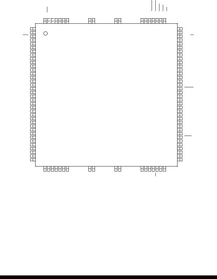
NC
VSS
FC0/CS3
FC1/CS4
FC2/CS5 ADDR19/CS6 ADDR20/CS7 ADDR21/CS8 ADDR22/CS9
ADDR23/CS10
VDD
VSS
T2CLK
TPUCH15
TPUCH14
TPUCH13
TPUCH12
NC
VDD
VSS
TPUCH11
TPUCH10
TPUCH9
TPUCH8 VDDE
VSSE
TPUCH7
TPUCH6
TPUCH5
TPUCH4
TPUCH3
TPUCH2
TPUCH1
TPUCH0 VSS NC
|
DD |
V |
|
|
|
|
|
|
|
1 |
144 |
|
|
2 |
|
3 |
|
4 |
|
5 |
|
6 |
|
7 |
|
8 |
|
9 |
|
10 |
|
11 |
|
12 |
|
13 |
|
14 |
|
15 |
|
16 |
|
17 |
|
18 |
|
19 |
|
20 |
|
21 |
|
22 |
|
23 |
|
24 |
|
25 |
|
26 |
|
27 |
|
28 |
|
29 |
|
30 |
|
31 |
|
32 |
|
33 |
|
34 |
|
35 |
|
36 |
37 |
|
|
|
|
|
|
|
|
|
DD |
V |
|
 143 BGACK/CS2
VSTBY 38
142 BG/CS1

ADDR1 39
141 BR/CS0

ADDR2 40
140 CSBOOT
ADDR3 41
139 DATA0
ADDR4 42
138 DATA1
ADDR5 43
137 DATA2
ADDR6 44
DATA3 |
V V |
DATA4 |
|
DATA5 |
||||
|
|
DD |
SS |
|
|
|
||
|
|
|
|
|
|
|
|
|
|
|
|
|
|
|
|
|
|
136 |
135 |
|
134 |
|
133 |
132 |
||
45 |
46 |
47 |
48 |
|
49 |
|||
|
|
|
|
|
|
|
|
|
|
|
|
|
|
|
|
|
|
|
|
|
|
|
|
|
|
|
ADDR7 |
|
ADDR8 |
V |
V |
ADDR9 |
|||
|
|
|
|
DD |
|
SS |
|
|
131 DATA6
ADDR10 50
130 DATA7
ADDR11 51
NC |
V |
DATA8 |
|
NC |
|
DATA9 |
||
|
|
SS |
|
|
|
|
|
|
|
|
|
|
|
|
|
|
|
|
|
|
|
|
|
|
|
|
129 |
128 |
|
127 |
126 |
125 |
|||
MC68332
52 |
53 |
54 |
|
55 |
56 |
|||
|
|
|
|
|
|
|
|
|
|
|
|
|
|
|
|
|
|
|
|
|
|
|
|
|
|
|
ADDR12 |
|
NC |
|
SS |
NC |
|
ADDR13 |
|
|
V |
|
||||||
124 DATA10
ADDR14 57
123 NC
ADDR15 58
DATA11 |
V |
V |
DATA12 |
|
DATA13 |
|||
|
|
DD |
SS |
|
|
|
||
|
|
|
|
|
|
|
|
|
|
|
|
|
|
|
|
|
|
122 |
121 |
|
120 |
|
119 |
118 |
||
59 |
60 |
61 |
62 |
|
63 |
|||
|
|
|
|
|
|
|
|
|
|
|
|
|
|
|
|
|
|
|
|
|
|
|
|
|
|
|
NC |
|
ADDR16 |
|
DD |
|
SS |
ADDR17 |
|
|
V |
V |
||||||
117 DATA14
ADDR18 64
116 DATA15
PQS0/MISO 65
115 ADDR0
PQS1/MOSI 66
114 PE0/DSACK0
PQS2/SCK 67
113 PE1/DSACK1
PQS3/PCS0/SS 68
112 PE2/AVEC
PQS4/PCS1 69
111 PE3/RMC
PQS5/PCS2 70
PE5/DS |
V |
|||
|
|
DD |
||
|
|
|
|
|
|
|
|
|
|
110 |
109 |
|||
108 |
||||
|
||||
|
107 |
|||
|
106 |
|||
|
105 |
|||
|
104 |
|||
|
103 |
|||
|
102 |
|||
|
101 |
|||
|
100 |
|||
|
99 |
|||
|
98 |
|||
|
97 |
|||
|
96 |
|||
|
95 |
|||
|
94 |
|||
|
93 |
|||
|
92 |
|||
|
91 |
|||
|
90 |
|||
|
89 |
|||
|
88 |
|||
|
87 |
|||
|
86 |
|||
|
85 |
|||
|
84 |
|||
|
83 |
|||
|
82 |
|||
|
81 |
|||
|
80 |
|||
|
79 |
|||
|
78 |
|||
|
77 |
|||
|
76 |
|||
|
75 |
|||
|
74 |
|||
|
73 |
|||
71 |
72 |
|
||
|
|
|
||
|
|
|
|
|
|
|
|
|
|
PQS6/PCS3 |
|
DD |
||
V |
||||
NC
VSS PE4/AS
PE6/SIZ0
PE7/SIZ1 R/W PF0/MODCLK PF1/IRQ1 PF2/IRQ2 PF3/IRQ3 PF4/IRQ4 PF5/IRQ5 PF6/IRQ6 PF7/IRQ7 BERR
HALT
RESET VSS
CLKOUT
VDD
NC
XFC
VDD
EXTAL
VDD
XTAL
VSS
FREEZE/QUOT TSC
BKPT/DSCLK IFETCH/DSI IPIPE/DSO RXD
PQS7/TXD VSS
NC
332 144-PIN QFP
Figure 3 MC68332 144-Pin QFP Pin Assignments
MOTOROLA |
MC68332 |
8 |
MC68332TS/D |

1.4 Address Map
The following figure is a map of the MCU internal addresses. The RAM array is positioned by the base address registers in the associated RAM control block. Unimplemented blocks are mapped externally.
$YFF000
$YFFA00 |
|
SIM |
|
|
|
|
|
|
|
|
|
|
|
|
|
|
|
|
|
|
|
|
|
$YFFA80 |
|
RESERVED |
|
|
|
|
|
|
|
|
|
|
|
|
|
|
|
|
|
|
|
|
|
$YFFB00 |
|
TPURAM CONTROL |
|
|
|
|
|
$YFFB40 |
|
|
|
|
|
|
|
|
|
|
|
|
|
|
|
|
RESERVED |
|
|
|
2-KBYTE |
|
|
|
|
|
|
|
|
||
|
|
|
|
|
|
|
|
$YFFC00 |
|
QSM |
|
|
|
TPURAM ARRAY |
|
|
|
|
|
|
|
|
|
|
|
|
|
||||
|
|
|
|
|
|
|
|
$YFFE00 |
|
TPU |
|
|
|
|
|
|
|
|
|
|
|
|
|
$YFFFFF |
|
|
|
|
|
|
|
|
|
|
|
|
|
332 ADDRESS MAP |
|
|
|
Figure 4 MCU Address Map |
|||||
1.5 Intermodule Bus |
|
|
|
|
|
|
|
The intermodule bus (IMB) is a standardized bus developed to facilitate both design and operation of modular microcontrollers. It contains circuitry to support exception processing, address space partitioning, multiple interrupt levels, and vectored interrupts. The standardized modules in the MCU communicate with one another and with external components through the IMB. The IMB in the MCU uses 24 address and 16 data lines.
MC68332 |
MOTOROLA |
MC68332TS/D |
9 |

2 Signal Descriptions
2.1 Pin Characteristics
The following table shows MCU pins and their characteristics. All inputs detect CMOS logic levels. All inputs can be put in a high-impedance state, but the method of doing this differs depending upon pin function. Refer to the table, MCU Driver Types, for a description of output drivers. An entry in the discrete I/O column of the MCU Pin Characteristics table indicates that a pin has an alternate I/O function. The port designation is given when it applies. Refer to the MCU Block Diagram for information about port organization.
Table 2 MCU Pin Characteristic
|
|
|
|
|
|
|
|
|
|
Pin |
Output |
Input |
Input |
Discrete |
Port |
||||||||||||||||||||||||||
|
|
Mnemonic |
Driver |
Synchronized |
Hysteresis |
I/O |
Designation |
||||||||||||||||||||||||||||||||||
|
|
|
|
|
|
|
|
|
|
|
|
|
|
|
|
|
|
|
|
|
|
|
|
|
|
|
|
|
|
|
|
|
|
|
|
|
|
|
|
|
|
|
|
|
|
|
|
|
|
|
|
|
|
|
|
|
|
|
|
|
|
|
|
|
|
|
|
|
|
|
|
|
|
|
|
|
|
|
A |
Y |
N |
O |
— |
ADDR23/CS10/ECLK |
|||||||||||||||||||||||||||||||||||||||||
|
|
|
|
|
|
|
|
|
|
|
|
|
|
|
|
|
|
|
|
|
|
|
|
|
|
|
|
|
|
|
|
|
|
|
|
|
|
|
|
|
|
|
|
|
|
|
|
|
|
|
|
|
|
|
|
|
|
|
|
|
|
|
|
|
|
|
|
|
|
|
|
|
|
|
|
|
|
|
A |
Y |
N |
O |
PC[6:3] |
ADDR[22:19]/CS[9:6] |
|||||||||||||||||||||||||||||||||||||||||
|
|
|
|
|
|
|
|
||||||||||||||||||||||||||||||||||
|
|
ADDR[18:0] |
A |
Y |
N |
— |
— |
||||||||||||||||||||||||||||||||||
|
|
|
|
|
|
|
|
|
|
|
|
|
|
|
|
|
|
|
|
|
|
|
|
|
|
|
|
|
|
|
|
|
|
|
|
|
|
|
|
|
|
|
|
|
|
|
|
|
|
|
|
|
|
|
|
|
|
|
|
|
|
|
|
|
|
|
|
|
|
|
|
|
|
|
|
|
|
B |
Y |
N |
I/O |
PE5 |
|
|
|
|
|
|
|
|
|
|
|
|
AS |
||||||||||||||||||||||||||||||
|
|
|
|
|
|
|
|
|
|
|
|
|
|
|
|
|
|
|
|
|
|
|
|
|
|
|
|
|
|
|
|
|
|
|
|
|
|
|
|
|
|
|
|
|
|
|
|
|
|
|
|
|
|
|
|
|
|
|
|
|
|
|
|
|
|
|
|
|
|
|
|
|
|
|
|
|
|
B |
Y |
N |
I/O |
PE2 |
|
|
|
|
|
|
|
|
AVEC |
||||||||||||||||||||||||||||||||||
|
|
|
|
|
|
|
|
|
|
|
|
|
|
|
|
|
|
|
|
|
|
|
|
|
|
|
|
|
|
|
|
|
|
|
|
|
|
|
|
||
|
|
|
|
|
|
|
|
|
|
|
|
|
|
|
|
|
|
|
|
|
|
|
|
|
|
|
|
|
|
|
|
|
|
|
|
B |
Y |
N |
— |
— |
|
|
|
|
|
|
|
|
BERR |
||||||||||||||||||||||||||||||||||
|
|
|
|
|
|
|
|
|
|
|
|
|
|
|
|
|
|
|
|
|
|
|
|
|
|
|
|
|
|
|
|
|
|
|
|
|
|||||
|
|
|
|
|
|
|
|
|
|
|
|
|
|
|
|
|
|
|
|
|
|
|
|
|
|
|
|
|
|
|
|
|
|
|
|
|
B |
— |
— |
— |
— |
|
|
|
|
|
BG/CS1 |
||||||||||||||||||||||||||||||||||||
|
|
|
|
|
|
|
|
|
|
|
|
|
|
|
|
|
|
|
|
|
|
|
|
|
|
|
|
|
|
|
|
|
|
|
|
||||||
|
|
|
|
|
|
|
|
|
|
|
|
|
|
|
|
|
|
|
|
|
|
|
|
|
|
|
|
|
|
|
|
|
|
|
|
|
B |
Y |
N |
— |
— |
|
|
BGACK/CS2 |
|||||||||||||||||||||||||||||||||||||||
|
|
|
|
|
|
|
|
|
|
|
|
|
|
|
|
|
|
|
|
|
|
|
|
|
|
|
|
|
|
|
|
|
|||||||||
|
|
|
|
|
|
|
|
|
|
|
|
|
|
|
|
|
|
|
|
|
|
|
|
|
|
|
|
|
|
|
|
|
|
|
|
|
— |
Y |
Y |
— |
— |
|
BKPT/DSCLK |
||||||||||||||||||||||||||||||||||||||||
|
|
|
|
|
|
|
|
|
|
|
|
|
|
|
|
|
|
|
|
|
|
|
|
|
|
|
|
|
|
|
|
|
|||||||||
|
|
|
|
|
|
|
|
|
|
|
|
|
|
|
|
|
|
|
|
|
|
|
|
|
|
|
|
|
|
|
|
|
|
|
|
|
B |
Y |
N |
— |
— |
|
|
|
|
|
BR/CS0 |
||||||||||||||||||||||||||||||||||||
|
|
|
|
|
|
|
|
|
|||||||||||||||||||||||||||||||||
|
|
|
CLKOUT |
A |
— |
— |
— |
— |
|||||||||||||||||||||||||||||||||
|
|
|
|
|
|
|
|
|
|
|
|
|
|
|
|
|
|
|
|
|
|
|
|
|
|
|
|
|
|
|
|
||||||||||
|
|
|
|
|
|
|
|
|
|
|
|
|
|
|
|
|
|
|
|
|
|
|
|
|
|
|
|
|
|
|
|
|
|
|
B |
— |
— |
— |
— |
||
|
|
|
CSBOOT |
||||||||||||||||||||||||||||||||||||||
|
|
|
|
|
|
|
|
||||||||||||||||||||||||||||||||||
|
|
DATA[15:0]1 |
Aw |
Y |
N |
— |
— |
||||||||||||||||||||||||||||||||||
|
|
|
|
|
|
|
|
|
|
|
|
|
|
|
|
|
|
|
|
|
|
|
|
|
|
|
|
|
|
|
|
B |
Y |
N |
I/O |
PE4 |
|||||
|
|
|
|
|
|
|
|
|
|
|
DS |
||||||||||||||||||||||||||||||
|
|
|
|
|
|
|
|
|
|
|
|
|
|
|
|
|
|
|
|
|
|
|
|
|
|
|
|
|
|||||||||||||
|
|
|
|
|
|
|
|
|
|
|
|
|
|
|
|
|
|
|
|
|
|
|
|
|
|
|
|
|
|
|
|
|
|
|
B |
Y |
N |
I/O |
PE1 |
||
|
|
|
|
|
DSACK1 |
||||||||||||||||||||||||||||||||||||
|
|
|
|
|
|
|
|
|
|
|
|
|
|
|
|
|
|
|
|
|
|
|
|
|
|
|
|||||||||||||||
|
|
|
|
|
|
|
|
|
|
|
|
|
|
|
|
|
|
|
|
|
|
|
|
|
|
|
|
|
|
|
|
|
B |
Y |
N |
I/O |
PE0 |
||||
|
|
|
|
DSACK0 |
|||||||||||||||||||||||||||||||||||||
|
|
|
|
|
|
|
|
|
|
|
|
|
|
|
|
|
|
|
|
|
|
|
|||||||||||||||||||
|
|
|
|
|
|
|
|
|
|
|
|
|
|
|
|
|
|
|
|
|
|
|
|
|
|
|
|
|
|
|
|
|
|
|
A |
Y |
Y |
— |
— |
||
|
|
DSI/IFETCH |
|||||||||||||||||||||||||||||||||||||||
|
|
|
|
|
|
|
|
|
|
|
|
|
|
|
|
|
|
|
|
|
|||||||||||||||||||||
|
|
|
|
|
|
|
|
|
|
|
|
|
|
|
|
|
|
|
|
|
|
|
|
|
|
|
|
|
|
|
|
|
|
A |
— |
— |
— |
— |
|||
|
|
DSO/IPIPE |
|||||||||||||||||||||||||||||||||||||||
|
|
|
|
|
|
|
|
|
|
|
|||||||||||||||||||||||||||||||
|
|
|
|
|
EXTAL2 |
— |
— |
Special |
— |
— |
|||||||||||||||||||||||||||||||
|
|
|
|
|
|
|
|
|
|
|
|
|
|
|
|
|
|
|
|
|
|
|
|
|
|
|
|
|
|
|
|
|
|
|
|
A |
Y |
N |
O |
PC[2:0] |
|
FC[2:0]/CS[5:3] |
|||||||||||||||||||||||||||||||||||||||||
|
|
|
|
|
|
||||||||||||||||||||||||||||||||||||
FREEZE/QUOT |
A |
— |
— |
— |
— |
||||||||||||||||||||||||||||||||||||
|
|
|
|
|
|
|
|
|
|
|
|
|
|
|
|
|
|
|
|
|
|
|
|||||||||||||||||||
|
|
|
|
|
|
|
|
|
|
|
|
|
|
|
|
|
|
|
|
|
|
|
|
|
|
|
Bo |
Y |
N |
— |
— |
||||||||||
|
|
|
|
|
|
|
|
HALT |
|||||||||||||||||||||||||||||||||
|
|
|
|
|
|
|
|
|
|
|
|
|
|
|
|
|
|
|
|
||||||||||||||||||||||
|
|
|
|
|
|
|
|
|
|
|
|
|
|
|
|
|
|
|
|
|
|
|
|
|
|
|
|
|
B |
Y |
Y |
I/O |
PF[7:1] |
||||||||
|
|
|
|
|
IRQ[7:1] |
||||||||||||||||||||||||||||||||||||
|
|
|
|
|
|
|
|
|
|
|
|
|
|
||||||||||||||||||||||||||||
|
|
|
|
|
|
|
|
MISO |
Bo |
Y |
Y |
I/O |
PQS0 |
||||||||||||||||||||||||||||
|
|
|
|
|
|
|
|
||||||||||||||||||||||||||||||||||
|
|
MODCLK1 |
B |
Y |
N |
I/O |
PF0 |
||||||||||||||||||||||||||||||||||
|
|
|
|
|
|
|
|
MOSI |
Bo |
Y |
Y |
I/O |
PQS1 |
||||||||||||||||||||||||||||
|
|
|
|
|
|
|
|
|
|
|
|
|
|
|
|
||||||||||||||||||||||||||
|
|
|
|
|
|
|
|
|
|
|
|
|
|
|
|
|
|
|
|
|
|
|
|
|
|
|
|
|
|
|
Bo |
Y |
Y |
I/O |
PQS3 |
||||||
|
|
|
PCS0/SS |
||||||||||||||||||||||||||||||||||||||
|
|
|
|
|
|
|
|
|
|
||||||||||||||||||||||||||||||||
|
|
|
|
PCS[3:1] |
Bo |
Y |
Y |
I/O |
PQS[6:4] |
||||||||||||||||||||||||||||||||
|
|
|
|
|
|
|
|
|
|
|
|
|
|
|
|
|
|
||||||||||||||||||||||||
|
|
|
|
|
|
|
|
|
|
|
|
|
|
|
|
|
|
|
|
|
|
|
|
A |
Y |
N |
— |
— |
|||||||||||||
|
|
|
|
|
|
|
|
|
R/W |
||||||||||||||||||||||||||||||||
|
|
|
|
|
|
|
|
|
|
|
|
|
|
|
|||||||||||||||||||||||||||
|
|
|
|
|
|
|
|
|
|
|
|
|
|
|
|
|
|
|
|
|
|
|
|
|
|
|
Bo |
Y |
Y |
— |
— |
||||||||||
|
|
|
|
|
|
RESET |
|||||||||||||||||||||||||||||||||||
|
|
|
|
|
|
|
|
|
|
|
|
|
|
|
|
||||||||||||||||||||||||||
|
|
|
|
|
|
|
|
|
|
|
|
|
|
|
|
|
|
|
|
|
|
|
B |
Y |
N |
I/O |
PE3 |
||||||||||||||
|
|
|
|
|
|
|
|
|
RMC |
||||||||||||||||||||||||||||||||
|
|
|
|
|
|
|
|
|
|
|
|
|
|
|
|||||||||||||||||||||||||||
|
|
|
|
|
|
|
|
|
RXD |
— |
N |
N |
— |
— |
|||||||||||||||||||||||||||
|
|
|
|
|
|
|
|
|
|
|
|
|
|
|
|||||||||||||||||||||||||||
|
|
|
|
|
|
|
|
|
SCK |
Bo |
Y |
Y |
I/O |
PQS2 |
|||||||||||||||||||||||||||
|
|
|
|
|
|
|
|
|
|
|
|||||||||||||||||||||||||||||||
|
|
|
|
|
SIZ[1:0] |
B |
Y |
N |
I/O |
PE[7:6] |
|||||||||||||||||||||||||||||||
|
|
|
|
|
|
|
|
|
|
|
|
|
|
|
|
|
|
|
|
|
|
|
|
|
|
|
|
|
|
|
|
|
|
|
|
|
|
|
|
|
|
MOTOROLA |
MC68332 |
10 |
MC68332TS/D |
Table 2 MCU Pin Characteristic (Continued)
Pin |
Output |
Input |
Input |
Discrete |
Port |
Mnemonic |
Driver |
Synchronized |
Hysteresis |
I/O |
Designation |
|
|
|
|
|
|
T2CLK |
— |
Y |
Y |
— |
— |
|
|
|
|
|
|
TPUCH[15:0] |
A |
Y |
Y |
— |
— |
|
|
|
|
|
|
TSC |
— |
Y |
Y |
— |
— |
|
|
|
|
|
|
TXD |
Bo |
Y |
Y |
I/O |
PQS7 |
|
|
|
|
|
|
XFC2 |
— |
— |
— |
Special |
— |
XTAL2 |
— |
— |
— |
Special |
— |
NOTES:
1.DATA[15:0] are synchronized during reset only. MODCLK is synchronized only when used as an input port pin.
2.EXTAL, XFC, and XTAL are clock reference connections.
2.2MCU Power Connections
|
Table 3 MCU Power Connections |
|
|
|
|
VSTBY |
|
Standby RAM Power/Clock Synthesizer Power |
VDDSYN |
|
Clock Synthesizer Power |
VSSE/VDDE |
|
External Periphery Power (Source and Drain) |
VSSI/VDDI |
|
Internal Module Power (Source and Drain) |
2.3 MCU Driver Types |
|
|
|
|
Table 4 MCU Driver Types |
|
|
|
Type |
I/O |
Description |
|
|
|
A |
O |
Output-only signals that are always driven; no external pull-up required |
|
|
|
Aw |
O |
Type A output with weak P-channel pull-up during reset |
|
|
|
B |
O |
Three-state output that includes circuitry to pull up output before high impedance is |
|
|
established, to ensure rapid rise time. An external holding resistor is required to maintain |
|
|
logic level while the pin is in the high-impedance state. |
|
|
|
Bo |
O |
Type B output that can be operated in an open-drain mode |
|
|
|
MC68332 |
MOTOROLA |
MC68332TS/D |
11 |

2.4 Signal Characteristics
Table 5 MCU Signal Characteristics
Signal Name |
MCU Module |
Signal Type |
Active State |
|||||||||||||||||||||||||||
|
|
|
|
|||||||||||||||||||||||||||
ADDR[23:0] |
SIM |
Bus |
— |
|||||||||||||||||||||||||||
|
|
|
|
|
|
|
|
|
|
|
|
|
|
|
|
|
|
|
|
|
|
|
|
|
|
|
|
|
|
|
|
|
|
|
|
|
|
|
|
|
|
|
|
|
|
|
|
|
|
|
|
|
|
|
|
|
|
|
SIM |
Output |
0 |
|
|
|
|
|
|
|
|
|
AS |
|||||||||||||||||||||
|
|
|
|
|
|
|
|
|
|
|
|
|
|
|
|
|
|
|
|
|
|
|
|
|
|
|
|
|
|
|
|
|
|
|
|
|
|
|
|
|
|
|
|
|
|
|
|
|
|
|
|
|
|
|
|
|
|
|
SIM |
Input |
0 |
AVEC |
||||||||||||||||||||||||||||||
|
|
|
|
|
|
|
|
|
|
|
|
|
|
|
|
|
|
|
|
|
|
|
|
|
|
|
|
|
||
|
|
|
|
|
|
|
|
|
|
|
|
|
|
|
|
|
|
|
|
|
|
|
|
|
|
|
|
SIM |
Input |
0 |
|
|
|
|
|
|
BERR |
||||||||||||||||||||||||
|
|
|
|
|
|
|
|
|
|
|
|
|
|
|
|
|
|
|
|
|
|
|
|
|
|
|
|
|||
|
|
|
|
|
|
|
|
|
|
|
|
|
|
|
|
|
|
|
|
|
|
|
|
|
|
SIM |
Output |
0 |
||
|
|
|
|
|
|
|
|
|
BG |
|||||||||||||||||||||
|
|
|
|
|
|
|
|
|
|
|
|
|
|
|
|
|
|
|
|
|
|
|
|
|
|
|||||
|
|
|
|
|
|
|
|
|
|
|
|
|
|
|
|
|
|
|
|
|
|
|
|
|
|
|
|
SIM |
Input |
0 |
BGACK |
||||||||||||||||||||||||||||||
|
|
|
|
|
|
|
|
|
|
|
|
|
|
|
|
|
|
|
|
|
|
|
|
|
|
|||||
|
|
|
|
|
|
|
|
|
|
|
|
|
|
|
|
|
|
|
|
|
|
|
|
|
CPU32 |
Input |
0 |
|||
|
|
|
|
|
|
|
BKPT |
|||||||||||||||||||||||
|
|
|
|
|
|
|
|
|
|
|
|
|
|
|
|
|
|
|
|
|
|
|
|
|
||||||
|
|
|
|
|
|
|
|
|
|
|
|
|
|
|
|
|
|
|
|
|
|
|
SIM |
Input |
0 |
|||||
|
|
|
|
|
|
|
|
|
BR |
|||||||||||||||||||||
|
|
|
|
|
|
|||||||||||||||||||||||||
|
|
CLKOUT |
SIM |
Output |
— |
|||||||||||||||||||||||||
|
|
|
|
|
|
|
|
|
|
|
|
|
|
|
|
|
|
|
|
|
|
|
||||||||
|
|
|
|
|
|
|
|
|
|
|
|
|
|
|
|
|
|
|
|
|
|
|
|
|
|
|
|
SIM |
Output |
0 |
|
|
|
CS[10:0] |
|||||||||||||||||||||||||||
|
|
|
|
|
|
|
|
|
|
|
|
|
|
|
|
|
|
|
|
|
|
|||||||||
|
|
|
|
|
|
|
|
|
|
|
|
|
|
|
|
|
|
|
|
|
|
|
|
|
|
|
|
SIM |
Output |
0 |
|
|
CSBOOT |
||||||||||||||||||||||||||||
|
|
|
|
|||||||||||||||||||||||||||
DATA[15:0] |
SIM |
Bus |
— |
|||||||||||||||||||||||||||
|
|
|
|
|
|
|
|
|
|
|
|
|
|
|
|
|
|
|
|
|
|
|||||||||
|
|
|
|
|
|
|
|
|
|
|
|
|
|
|
|
|
|
|
|
|
SIM |
Output |
0 |
|||||||
|
|
|
|
|
|
|
|
|
DS |
|||||||||||||||||||||
|
|
|
|
|
|
|
|
|
|
|
|
|
|
|
|
|
|
|
||||||||||||
|
|
|
|
|
|
|
|
|
|
|
|
|
|
|
|
|
|
|
|
|
|
|
|
|
|
|
|
SIM |
Input |
0 |
|
DSACK[1:0] |
|||||||||||||||||||||||||||||
|
|
|
|
|
|
|
|
|
||||||||||||||||||||||
|
|
|
|
|
DSCLK |
CPU32 |
Input |
Serial Clock |
||||||||||||||||||||||
|
|
|
|
|
|
|
|
|
|
|
|
|||||||||||||||||||
|
|
|
|
|
|
|
|
DSI |
CPU32 |
Input |
(Serial Data) |
|||||||||||||||||||
|
|
|
|
|
|
|
|
|
|
|
|
|||||||||||||||||||
|
|
|
|
|
|
|
|
DSO |
CPU32 |
Output |
(Serial Data) |
|||||||||||||||||||
|
|
|
|
|
|
|
|
|
||||||||||||||||||||||
|
|
|
|
|
EXTAL |
SIM |
Input |
— |
||||||||||||||||||||||
|
|
|
|
|
|
|
|
|
||||||||||||||||||||||
|
|
|
|
|
FC[2:0] |
SIM |
Output |
— |
||||||||||||||||||||||
|
|
|
|
|
|
|||||||||||||||||||||||||
|
|
FREEZE |
SIM |
Output |
1 |
|||||||||||||||||||||||||
|
|
|
|
|
|
|
|
|
|
|
|
|
|
|
|
|
|
|
|
|||||||||||
|
|
|
|
|
|
|
|
|
|
|
|
|
|
|
|
|
|
|
|
|
SIM |
Input/Output |
0 |
|||||||
|
|
|
|
|
|
|
HALT |
|||||||||||||||||||||||
|
|
|
|
|
|
|
|
|
|
|
|
|
|
|
|
|
|
|||||||||||||
|
|
|
|
|
|
|
|
|
|
|
|
|
|
|
|
|
|
|
|
|
|
|
|
|
CPU32 |
Output |
— |
|||
|
|
|
|
IFETCH |
||||||||||||||||||||||||||
|
|
|
|
|
|
|
|
|
|
|
|
|
|
|
|
|
|
|
||||||||||||
|
|
|
|
|
|
|
|
|
|
|
|
|
|
|
|
|
|
|
|
CPU32 |
Output |
— |
||||||||
|
|
|
|
|
|
|
IPIPE |
|||||||||||||||||||||||
|
|
|
|
|
|
|
|
|
|
|
|
|
|
|
||||||||||||||||
|
|
|
|
|
|
|
|
|
|
|
|
|
|
|
|
|
|
|
|
|
|
|
|
|
SIM |
Input |
0 |
|||
|
|
|
IRQ[7:1] |
|||||||||||||||||||||||||||
|
|
|
|
|
|
|
|
|
|
|
||||||||||||||||||||
|
|
|
|
|
|
|
MISO |
QSM |
Input/Output |
— |
||||||||||||||||||||
|
|
|
|
|
||||||||||||||||||||||||||
|
MODCLK |
SIM |
Input |
— |
||||||||||||||||||||||||||
|
|
|
|
|
|
|
|
|
|
|
||||||||||||||||||||
|
|
|
|
|
|
|
MOSI |
QSM |
Input/Output |
— |
||||||||||||||||||||
|
|
|
|
|
|
|
|
|
||||||||||||||||||||||
|
|
|
|
|
PC[6:0] |
SIM |
Output |
(Port) |
||||||||||||||||||||||
|
|
|
|
|
|
|||||||||||||||||||||||||
|
|
PCS[3:0] |
QSM |
Input/Output |
— |
|||||||||||||||||||||||||
|
|
|
|
|
|
|
|
|
||||||||||||||||||||||
|
|
|
|
|
PE[7:0] |
SIM |
Input/Output |
(Port) |
||||||||||||||||||||||
|
|
|
|
|
|
|
|
|
||||||||||||||||||||||
|
|
|
|
|
PF[7:0] |
SIM |
Input/Output |
(Port) |
||||||||||||||||||||||
|
|
|
|
|
|
|||||||||||||||||||||||||
|
|
PQS[7:0] |
QSM |
Input/Output |
(Port) |
|||||||||||||||||||||||||
|
|
|
|
|
|
|
|
|
||||||||||||||||||||||
|
|
|
|
|
QUOT |
SIM |
Output |
— |
||||||||||||||||||||||
|
|
|
|
|
|
|
|
|
|
|
|
|
|
|
||||||||||||||||
|
|
|
|
|
|
|
|
|
|
|
|
|
|
|
|
|
|
|
|
|
|
SIM |
Input/Output |
0 |
||||||
|
|
|
|
|
RESET |
|||||||||||||||||||||||||
|
|
|
|
|
|
|
|
|
|
|
|
|
|
|
|
|||||||||||||||
|
|
|
|
|
|
|
|
|
|
|
|
|
|
|
|
|
SIM |
Output |
0 |
|||||||||||
|
|
|
|
|
|
|
|
RMC |
||||||||||||||||||||||
|
|
|
|
|
|
|
|
|
|
|
|
|
|
|||||||||||||||||
|
|
|
|
|
|
|
|
|
|
|
|
|
|
|
|
SIM |
Output |
1/0 |
||||||||||||
|
|
|
|
|
|
|
|
R/W |
||||||||||||||||||||||
|
|
|
|
|
|
|
|
|
|
|
|
|||||||||||||||||||
|
|
|
|
|
|
|
|
RXD |
QSM |
Input |
— |
|||||||||||||||||||
|
|
|
|
|
|
|
|
|
|
|
|
|||||||||||||||||||
|
|
|
|
|
|
|
|
SCK |
QSM |
Input/Output |
— |
|||||||||||||||||||
|
|
|
|
|
|
|
|
|||||||||||||||||||||||
|
|
|
|
SIZ[1:0] |
SIM |
Output |
— |
|||||||||||||||||||||||
|
|
|
|
|
|
|
|
|
|
|
|
|
|
|||||||||||||||||
|
|
|
|
|
|
|
|
|
|
|
|
QSM |
Input |
0 |
||||||||||||||||
|
|
|
|
|
|
|
|
|
SS |
|||||||||||||||||||||
|
|
|
|
|
|
|
|
|
||||||||||||||||||||||
|
|
|
|
|
T2CLK |
TPU |
Input |
— |
||||||||||||||||||||||
|
|
|
|
|||||||||||||||||||||||||||
TPUCH[15:0] |
TPU |
Input/Output |
1 |
|||||||||||||||||||||||||||
|
|
|
|
|
|
|
|
|
|
|
|
|
|
|
|
|
|
|
|
|
|
|
|
|
|
|
|
|
|
|
MOTOROLA |
MC68332 |
12 |
MC68332TS/D |

Table 5 MCU Signal Characteristics (Continued)
Signal Name |
MCU Module |
Signal Type |
Active State |
|
|
|
|
TSC |
SIM |
Input |
— |
|
|
|
|
TXD |
QSM |
Output |
— |
|
|
|
|
XFC |
SIM |
Input |
— |
|
|
|
|
XTAL |
SIM |
Output |
— |
|
|
|
|
2.5 Signal Function
Table 6 MCU Signal Function
Signal Name |
|
Mnemonic |
Function |
||||||||||||||||||||
|
|
|
|
||||||||||||||||||||
Address Bus |
|
ADDR[23:0] |
24-bit address bus |
||||||||||||||||||||
|
|
|
|
|
|
|
|
|
|
|
|
|
|
|
|
|
|
|
|
|
|
|
|
Address Strobe |
|
|
|
|
|
|
|
|
|
|
|
|
|
|
|
|
|
|
|
|
|
|
Indicates that a valid address is on the address bus |
|
|
|
|
|
|
|
AS |
||||||||||||||||
|
|
|
|
|
|
|
|
|
|
|
|
|
|
|
|
|
|
|
|
|
|
|
|
Autovector |
|
|
|
|
|
|
|
|
|
|
|
|
|
|
|
|
|
|
|
|
|
|
Requests an automatic vector during interrupt acknowledge |
|
|
|
|
|
AVEC |
||||||||||||||||||
|
|
|
|
|
|
|
|
|
|
|
|
|
|
|
|
|
|
|
|
|
|
||
Bus Error |
|
|
|
|
|
|
|
|
|
|
|
|
|
|
|
|
|
|
|
|
|
|
Indicates that a bus error has occurred |
|
|
|
|
|
BERR |
||||||||||||||||||
|
|
|
|
|
|
|
|
|
|
|
|
|
|
|
|
|
|
|
|
|
|||
Bus Grant |
|
|
|
|
|
|
|
|
|
|
|
|
|
|
|
|
|
|
|
|
Indicates that the MCU has relinquished the bus |
||
|
|
|
|
|
|
|
BG |
||||||||||||||||
|
|
|
|
|
|
|
|
|
|
|
|
|
|
|
|
|
|
|
|
||||
Bus Grant Acknowledge |
|
|
|
|
|
|
|
|
|
|
|
|
|
|
|
|
|
|
|
|
|
|
Indicates that an external device has assumed bus mastership |
|
|
|
|
BGACK |
|||||||||||||||||||
|
|
|
|
|
|
|
|
|
|
|
|
|
|
|
|
|
|
|
|||||
Breakpoint |
|
|
|
|
|
|
|
|
|
|
|
|
|
|
|
|
|
|
|
Signals a hardware breakpoint to the CPU |
|||
|
|
|
|
|
BKPT |
||||||||||||||||||
|
|
|
|
|
|
|
|
|
|
|
|
|
|
|
|
|
|
||||||
Bus Request |
|
|
|
|
|
|
|
|
|
|
|
|
|
|
|
|
|
Indicates that an external device requires bus mastership |
|||||
|
|
|
|
|
|
|
BR |
||||||||||||||||
|
|
|
|
|
|||||||||||||||||||
System Clockout |
|
|
CLKOUT |
System clock output |
|||||||||||||||||||
|
|
|
|
|
|
|
|
|
|
|
|
|
|
|
|||||||||
Chip Selects |
|
|
|
|
|
|
|
|
|
|
|
|
|
|
|
|
|
|
|
|
|
|
Select external devices at programmed addresses |
|
|
|
CS[10:0] |
||||||||||||||||||||
|
|
|
|
|
|
|
|
|
|
|
|
|
|
||||||||||
Boot Chip Select |
|
|
|
|
|
|
|
|
|
|
|
|
|
|
|
|
|
|
|
|
|
|
Chip select for external boot start-up ROM |
|
|
CSBOOT |
|||||||||||||||||||||
|
|
|
|
||||||||||||||||||||
Data Bus |
|
DATA[15:0] |
16-bit data bus |
||||||||||||||||||||
|
|
|
|
|
|
|
|
|
|
|
|
|
|
|
|
||||||||
Data Strobe |
|
|
|
|
|
|
|
|
|
|
|
|
|
|
|
During a read cycle, indicates when it is possible for an external |
|||||||
|
|
|
|
|
|
|
DS |
||||||||||||||||
|
|
|
|
|
|
|
|
|
|
|
|
|
|
|
|
|
|
|
|
|
|
|
device to place data on the data bus. During a write cycle, indi- |
|
|
|
|
|
|
|
|
|
|
|
|
|
|
|
|
|
|
|
|
|
|
|
cates that valid data is on the data bus. |
|
|
|
|
|
|
|
|
|
|
|
|
||||||||||||
Data and Size Acknowledge |
|
|
|
|
|
|
|
|
|
|
|
|
|
|
|
|
|
|
|
|
|
|
Provide asynchronous data transfers and dynamic bus sizing |
|
DSACK[1:0] |
||||||||||||||||||||||
|
|
|
|
||||||||||||||||||||
Development Serial In, Out, |
|
DSI, DSO, |
Serial I/O and clock for background debugging mode |
||||||||||||||||||||
Clock |
|
|
|
|
DSCLK |
|
|||||||||||||||||
|
|
|
|||||||||||||||||||||
Crystal Oscillator |
EXTAL, XTAL |
Connections for clock synthesizer circuit reference; |
|||||||||||||||||||||
|
|
|
|
|
|
|
|
|
|
|
|
|
|
|
|
|
|
|
|
|
|
|
a crystal or an external oscillator can be used |
|
|
|
|
|
|
|
|||||||||||||||||
Function Codes |
|
|
|
|
FC[2:0] |
Identify processor state and current address space |
|||||||||||||||||
|
|
|
|
|
|||||||||||||||||||
Freeze |
|
|
FREEZE |
Indicates that the CPU has entered background mode |
|||||||||||||||||||
|
|
|
|
|
|
|
|
|
|
|
|
|
|||||||||||
Halt |
|
|
|
|
|
|
|
|
|
|
|
|
|
|
|
Suspend external bus activity |
|||||||
|
|
|
|
|
|
HALT |
|||||||||||||||||
|
|
|
|
|
|
|
|
|
|
|
|||||||||||||
Instruction Pipeline |
|
|
|
|
|
|
|
|
|
|
|
|
|
|
|
|
|
|
|
Indicate instruction pipeline activity |
|||
|
|
|
|
IFETCH |
|||||||||||||||||||
|
|
|
|
|
|
|
IPIPE |
|
|
|
|||||||||||||
|
|
|
|
|
|
|
|||||||||||||||||
Interrupt Request Level |
|
|
|
|
|
|
|
|
|
|
|
|
|
|
|
|
|
|
|
Provides an interrupt priority level to the CPU |
|||
|
|
|
IRQ[7:1] |
||||||||||||||||||||
|
|
|
|
|
|
|
|
|
|||||||||||||||
Master In Slave Out |
|
|
|
|
|
|
MISO |
Serial input to QSPI in master mode; |
|||||||||||||||
|
|
|
|
|
|
|
|
|
|
|
|
|
|
|
|
|
|
|
|
|
|
|
serial output from QSPI in slave mode |
|
|
|
|
||||||||||||||||||||
Clock Mode Select |
|
MODCLK |
Selects the source and type of system clock |
||||||||||||||||||||
|
|
|
|
|
|
|
|
|
|||||||||||||||
Master Out Slave In |
|
|
|
|
|
|
MOSI |
Serial output from QSPI in master mode; |
|||||||||||||||
|
|
|
|
|
|
|
|
|
|
|
|
|
|
|
|
|
|
|
|
|
|
|
serial input to QSPI in slave mode |
|
|
|
|
|
|
|
|||||||||||||||||
Port C |
|
|
|
|
PC[6:0] |
SIM digital output port signals |
|||||||||||||||||
|
|
|
|
|
|||||||||||||||||||
Peripheral Chip Select |
|
|
PCS[3:0] |
QSPI peripheral chip selects |
|||||||||||||||||||
|
|
|
|
|
|
|
|||||||||||||||||
Port E |
|
|
|
|
PE[7:0] |
SIM digital I/O port signals |
|||||||||||||||||
|
|
|
|
|
|
|
|||||||||||||||||
Port F |
|
|
|
|
PF[7:0] |
SIM digital I/O port signals |
|||||||||||||||||
|
|
|
|
|
|||||||||||||||||||
Port QS |
|
|
PQS[7:0] |
QSM digital I/O port signals |
|||||||||||||||||||
|
|
|
|
|
|
|
|
|
|
|
|
|
|
|
|
|
|
|
|
|
|
|
|
MC68332 |
MOTOROLA |
MC68332TS/D |
13 |

Table 6 MCU Signal Function (Continued)
Signal Name |
Mnemonic |
Function |
||||||||
|
|
|
|
|||||||
Quotient Out |
|
QUOT |
Provides the quotient bit of the polynomial divider |
|||||||
|
|
|
|
|
|
|
|
|
|
|
Reset |
|
|
|
|
|
|
|
|
|
System reset |
|
RESET |
|||||||||
|
|
|
|
|
|
|
|
|
|
|
Read-Modify-Write Cycle |
|
|
|
|
|
|
|
|
Indicates an indivisible read-modify-write instruction |
|
|
|
RMC |
||||||||
|
|
|
|
|
|
|
|
|||
Read/Write |
|
|
|
|
|
|
|
|
|
Indicates the direction of data transfer on the bus |
|
|
R/W |
|
|||||||
|
|
|
|
|
||||||
SCI Receive Data |
|
|
RXD |
Serial input to the SCI |
||||||
|
|
|
|
|
||||||
QSPI Serial Clock |
|
|
SCK |
Clock output from QSPI in master mode; |
||||||
|
|
|
|
|
|
|
|
|
|
clock input to QSPI in slave mode |
|
|
|
||||||||
Size |
SIZ[1:0] |
Indicates the number of bytes to be transferred during a bus cycle |
||||||||
|
|
|
|
|
|
|
||||
Slave Select |
|
|
|
|
|
|
Causes serial transmission when QSPI is in slave mode; |
|||
|
|
|
SS |
|||||||
|
|
|
|
|
|
|
|
|
|
causes mode fault in master mode |
|
|
|
|
|||||||
TCR2 Clock |
|
T2CLK |
External clock source for TCR2 counter |
|||||||
|
|
|
||||||||
TPU Channel Pins |
TPUCH[15:0] |
Bidirectional pins associated with TPU channels |
||||||||
|
|
|
|
|
||||||
Three-State Control |
|
|
TSC |
Places all output drivers in a high-impedance state |
||||||
|
|
|
|
|
||||||
SCI Transmit Data |
|
|
TXD |
Serial output from the SCI |
||||||
|
|
|
|
|
||||||
External Filter Capacitor |
|
|
XFC |
Connection for external phase-locked loop filter capacitor |
||||||
|
|
|
|
|
|
|
|
|
|
|
MOTOROLA |
MC68332 |
14 |
MC68332TS/D |

3 System Integration Module
The MCU system integration module (SIM) consists of five functional blocks that control system startup, initialization, configuration, and external bus.
SYSTEM CONFIGURATION
AND PROTECTION
CLKOUT
CLOCK SYNTHESIZER  EXTAL
EXTAL
MODCLK
CHIP SELECTS |
|
CHIP SELECTS |
|
||
|
||
|
|
|
|
|
|
|
|
|
EXTERNAL BUS
EXTERNAL BUS INTERFACE
RESET
TSC
FACTORY TEST
FREEZE/QUOT
S(C)IM BLOCK
Figure 5 SIM Block Diagram
3.1 Overview
The system configuration and protection block controls MCU configuration and operating mode. The block also provides bus and software watchdog monitors.
The system clock generates clock signals used by the SIM, other IMB modules, and external devices. In addition, a periodic interrupt generator supports execution of time-critical control routines.
The external bus interface handles the transfer of information between IMB modules and external address space.
The chip-select block provides eleven general-purpose chip-select signals and a boot ROM chip select signal. Both general-purpose and boot ROM chip-select signals have associated base address registers and option registers.
The system test block incorporates hardware necessary for testing the MCU. It is used to perform factory tests, and its use in normal applications is not supported.
The SIM control register address map occupies 128 bytes. Unused registers within the 128-byte address space return zeros when read. The “Access” column in the SIM address map below indicates which registers are accessible only at the supervisor privilege level and which can be assigned to either the supervisor or user privilege level, according to the value of the SUPV bit in the SIMCR.
MC68332 |
MOTOROLA |
MC68332TS/D |
15 |
Table 7 SIM Address Map
|
Access |
Address |
15 |
8 |
7 |
0 |
|
|
|
|
|
|
|
|
|
|
S |
$YFFA00 |
|
SIM CONFIGURATION (SIMCR) |
|
|
|
|
|
|
|
|
|
|
|
|
S |
$YFFA02 |
|
FACTORY TEST (SIMTR) |
|
|
|
|
|
|
|
|
|
|
|
|
S |
$YFFA04 |
|
CLOCK SYNTHESIZER CONTROL (SYNCR) |
|
|
|
|
|
|
|
|
|
|
|
|
S |
$YFFA06 |
|
NOT USED |
RESET STATUS REGISTER (RSR) |
|
|
|
|
|
|
|
|
|
|
|
S |
$YFFA08 |
|
MODULE TEST E (SIMTRE) |
|
|
|
|
|
|
|
|
|
|
|
|
S |
$YFFA0A |
|
NOT USED |
NOT USED |
|
|
|
|
|
|
|
|
|
|
|
S |
$YFFA0C |
|
NOT USED |
NOT USED |
|
|
|
|
|
|
|
|
|
|
|
S |
$YFFA0E |
|
NOT USED |
NOT USED |
|
|
|
|
|
|
|
|
|
|
|
S/U |
$YFFA10 |
|
NOT USED |
PORT E DATA (PORTE0) |
|
|
|
|
|
|
|
|
|
|
|
S/U |
$YFFA12 |
|
NOT USED |
PORT E DATA (PORTE1) |
|
|
|
|
|
|
|
|
|
|
|
S/U |
$YFFA14 |
|
NOT USED |
PORT E DATA DIRECTION (DDRE) |
|
|
|
|
|
|
|
|
|
|
|
S |
$YFFA16 |
|
NOT USED |
PORT E PIN ASSIGNMENT (PEPAR) |
|
|
|
|
|
|
|
|
|
|
|
S/U |
$YFFA18 |
|
NOT USED |
PORT F DATA (PORTF0) |
|
|
|
|
|
|
|
|
|
|
|
S/U |
$YFFA1A |
|
NOT USED |
PORT F DATA (PORTF1) |
|
|
|
|
|
|
|
|
|
|
|
S/U |
$YFFA1C |
|
NOT USED |
PORT F DATA DIRECTION (DDRF) |
|
|
|
|
|
|
|
|
|
|
|
S |
$YFFA1E |
|
NOT USED |
PORT F PIN ASSIGNMENT (PFPAR) |
|
|
|
|
|
|
|
|
|
|
|
S |
$YFFA20 |
|
NOT USED |
SYSTEM PROTECTION CONTROL |
|
|
|
|
|
|
|
(SYPCR) |
|
|
|
|
|
|
|
|
|
|
|
S |
$YFFA22 |
|
PERIODIC INTERRUPT CONTROL (PICR) |
|
|
|
|
|
|
|
|
|
|
|
|
S |
$YFFA24 |
|
PERIODIC INTERRUPT TIMING (PITR) |
|
|
|
|
|
|
|
|
|
|
|
|
S |
$YFFA26 |
|
NOT USED |
SOFTWARE SERVICE (SWSR) |
|
|
|
|
|
|
|
|
|
|
|
S |
$YFFA28 |
|
NOT USED |
NOT USED |
|
|
|
|
|
|
|
|
|
|
|
S |
$YFFA2A |
|
NOT USED |
NOT USED |
|
|
|
|
|
|
|
|
|
|
|
S |
$YFFA2C |
|
NOT USED |
NOT USED |
|
|
|
|
|
|
|
|
|
|
|
S |
$YFFA2E |
|
NOT USED |
NOT USED |
|
|
|
|
|
|
|
|
|
|
|
S |
$YFFA30 |
|
TEST MODULE MASTER SHIFT A (TSTMSRA) |
|
|
|
|
|
|
|
|
|
|
|
|
S |
$YFFA32 |
|
TEST MODULE MASTER SHIFT B (TSTMSRB) |
|
|
|
|
|
|
|
|
|
|
|
|
S |
$YFFA34 |
|
TEST MODULE SHIFT COUNT (TSTSC) |
|
|
|
|
|
|
|
|
|
|
|
|
S |
$YFFA36 |
|
TEST MODULE REPETITION COUNTER (TSTRC) |
|
|
|
|
|
|
|
|
|
|
|
|
S |
$YFFA38 |
|
TEST MODULE CONTROL (CREG) |
|
|
|
|
|
|
|
|
|
|
|
|
S/U |
$YFFA3A |
|
TEST MODULE DISTRIBUTED REGISTER (DREG) |
|
|
|
|
|
|
|
|
|
|
|
|
|
$YFFA3C |
|
NOT USED |
NOT USED |
|
|
|
|
|
|
|
|
|
|
|
|
$YFFA3E |
|
NOT USED |
NOT USED |
|
|
|
|
|
|
|
|
|
|
|
S/U |
$YFFA40 |
|
NOT USED |
PORT C DATA (PORTC) |
|
|
|
|
|
|
|
|
|
|
|
|
$YFFA42 |
|
NOT USED |
NOT USED |
|
|
|
|
|
|
|
|
|
|
|
S |
$YFFA44 |
|
CHIP-SELECT PIN ASSIGNMENT (CSPAR0) |
|
|
|
|
|
|
|
|
|
|
|
|
S |
$YFFA46 |
|
CHIP-SELECT PIN ASSIGNMENT (CSPAR1) |
|
|
|
|
|
|
|
|
|
|
|
|
S |
$YFFA48 |
|
CHIP-SELECT BASE BOOT (CSBARBT) |
|
|
|
|
|
|
|
|
|
|
|
|
S |
$YFFA4A |
|
CHIP-SELECT OPTION BOOT (CSORBT) |
|
|
|
|
|
|
|
|
|
|
|
|
S |
$YFFA4C |
|
CHIP-SELECT BASE 0 (CSBAR0) |
|
|
|
|
|
|
|
|
|
|
|
|
S |
$YFFA4E |
|
CHIP-SELECT OPTION 0 (CSOR0) |
|
|
|
|
|
|
|
|
|
|
|
|
S |
$YFFA50 |
|
CHIP-SELECT BASE 1 (CSBAR1) |
|
|
|
|
|
|
|
|
|
|
|
|
S |
$YFFA52 |
|
CHIP-SELECT OPTION 1 (CSOR1) |
|
|
|
|
|
|
|
|
|
|
|
|
S |
$YFFA54 |
|
CHIP-SELECT BASE 2 (CSBAR2) |
|
|
|
|
|
|
|
|
|
|
|
|
|
|
|
|
|
|
|
|
|
|
|
|
|
|
|
MOTOROLA |
MC68332 |
16 |
MC68332TS/D |

Table 7 SIM Address Map (Continued)
Access |
Address |
15 |
8 |
7 |
|
0 |
|
|
|
|
|
|
|
S |
$YFFA56 |
|
CHIP-SELECT OPTION 2 |
(CSOR2) |
||
|
|
|
|
|
||
S |
$YFFA58 |
|
CHIP-SELECT BASE 3 |
(CSBAR3) |
||
|
|
|
|
|
||
S |
$YFFA5A |
|
CHIP-SELECT OPTION 3 |
(CSOR3) |
||
|
|
|
|
|
||
S |
$YFFA5C |
|
CHIP-SELECT BASE 4 |
(CSBAR4) |
||
|
|
|
|
|
||
S |
$YFFA5E |
|
CHIP-SELECT OPTION 4 |
(CSOR4) |
||
|
|
|
|
|
||
S |
$YFFA60 |
|
CHIP-SELECT BASE 5 |
(CSBAR5) |
||
|
|
|
|
|
||
S |
$YFFA62 |
|
CHIP-SELECT OPTION 5 |
(CSOR5) |
||
|
|
|
|
|
||
S |
$YFFA64 |
|
CHIP-SELECT BASE 6 |
(CSBAR6) |
||
|
|
|
|
|
||
S |
$YFFA66 |
|
CHIP-SELECT OPTION 6 |
(CSOR6) |
||
|
|
|
|
|
||
S |
$YFFA68 |
|
CHIP-SELECT BASE 7 |
(CSBAR7) |
||
|
|
|
|
|
||
S |
$YFFA6A |
|
CHIP-SELECT OPTION 7 |
(CSOR7) |
||
|
|
|
|
|
||
S |
$YFFA6C |
|
CHIP-SELECT BASE 8 |
(CSBAR8) |
||
|
|
|
|
|
||
S |
$YFFA6E |
|
CHIP-SELECT OPTION 8 |
(CSOR8) |
||
|
|
|
|
|
||
S |
$YFFA70 |
|
CHIP-SELECT BASE 9 |
(CSBAR9) |
||
|
|
|
|
|
||
S |
$YFFA72 |
|
CHIP-SELECT OPTION 9 |
(CSOR9) |
||
|
|
|
|
|
||
S |
$YFFA74 |
|
CHIP-SELECT BASE 10 |
(CSBAR10) |
||
|
|
|
|
|
||
S |
$YFFA76 |
|
CHIP-SELECT OPTION 10 |
(CSOR10) |
||
|
|
|
|
|
|
|
|
$YFFA78 |
|
NOT USED |
|
|
NOT USED |
|
|
|
|
|
|
|
|
$YFFA7A |
|
NOT USED |
|
|
NOT USED |
|
|
|
|
|
|
|
|
$YFFA7C |
|
NOT USED |
|
|
NOT USED |
|
|
|
|
|
|
|
|
$YFFA7E |
|
NOT USED |
|
|
NOT USED |
|
|
|
|
|
|
|
Y = M111, where M is the logic state of the module mapping (MM) bit in the SIMCR.
3.2 System Configuration and Protection
This functional block provides configuration control for the entire MCU. It also performs interrupt arbitration, bus monitoring, and system test functions. MCU system protection includes a bus monitor, a HALT monitor, a spurious interrupt monitor, and a software watchdog timer. These functions have been made integral to the microcontroller to reduce the number of external components in a complete control system.
MC68332 |
MOTOROLA |
MC68332TS/D |
17 |
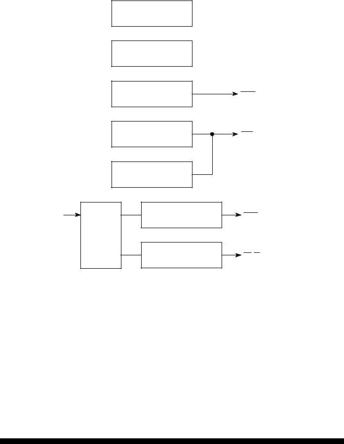
MODULE CONFIGURATION
AND TEST
RESET STATUS
HALT MONITOR |
RESET REQUEST |
|
BUS MONITOR |
BERR |
|
SPURIOUS INTERRUPT MONITOR |
|
CLOCK |
SOFTWARE WATCHDOG TIMER |
RESET REQUEST |
|
29 |
|
|
PRESCALER |
|
|
PERIODIC INTERRUPT TIMER |
IRQ [7:1] |
SYS PROTECT BLOCK
Figure 6 System Configuration and Protection Block
3.2.1 System Configuration
The SIM controls MCU configuration during normal operation and during internal testing.
SIMCR —SIM Configuration Register |
|
|
|
|
|
|
|
|
|
$YFFA00 |
||||||
15 |
14 |
13 |
12 |
11 |
|
10 |
9 |
8 |
7 |
6 |
5 |
4 |
3 |
|
|
0 |
|
|
|
|
|
|
|
|
|
|
|
|
|
|
|
|
|
EXOFF |
FRZSW |
FRZBM |
0 |
SLVEN |
|
0 |
SHEN |
|
SUPV |
MM |
0 |
0 |
|
|
IARB |
|
|
|
|
|
|
|
|
|
|
|
|
|
|
|
|
|
|
RESET: |
|
|
|
|
|
|
|
|
|
|
|
|
|
|
|
|
0 |
0 |
0 |
0 |
DATA11 |
0 |
0 |
0 |
1 |
1 |
0 |
0 |
1 |
1 |
1 |
1 |
|
The SIM configuration register controls system configuration. It can be read or written at any time, except for the module mapping (MM) bit, which can be written only once.
MOTOROLA |
MC68332 |
18 |
MC68332TS/D |

EXOFF — External Clock Off
0 = The CLKOUT pin is driven from an internal clock source. 1 = The CLKOUT pin is placed in a high-impedance state.
FRZSW — Freeze Software Enable
0 = When FREEZE is asserted, the software watchdog and periodic interrupt timer counters continue to run.
1 = When FREEZE is asserted, the software watchdog and periodic interrupt timer counters are disabled, preventing interrupts during software debug.
FRZBM — Freeze Bus Monitor Enable
0 = When FREEZE is asserted, the bus monitor continues to operate. 1 = When FREEZE is asserted, the bus monitor is disabled.
SLVEN — Factory Test Mode Enabled
This bit is a read-only status bit that reflects the state of DATA11 during reset. 0 = IMB is not available to an external master.
1 = An external bus master has direct access to the IMB.
SHEN[1:0] — Show Cycle Enable
This field determines what the EBI does with the external bus during internal transfer operations. A show cycle allows internal transfers to be externally monitored. The table below shows whether show cycle data is driven externally, and whether external bus arbitration can occur. To prevent bus conflict, external peripherals must not be enabled during show cycles.
SHEN |
Action |
|
|
00 |
Show cycles disabled, external arbitration enabled |
|
|
01 |
Show cycles enabled, external arbitration disabled |
|
|
10 |
Show cycles enabled, external arbitration enabled |
|
|
11 |
Show cycles enabled, external arbitration enabled, |
|
internal activity is halted by a bus grant |
|
|
SUPV — Supervisor/Unrestricted Data Space
The SUPV bit places the SIM global registers in either supervisor or user data space.
0 = Registers with access controlled by the SUPV bit are accessible from either the user or supervisor privilege level.
1 = Registers with access controlled by the SUPV bit are restricted to supervisor access only.
MM — Module Mapping
0 = Internal modules are addressed from $7FF000 –$7FFFFF. 1 = Internal modules are addressed from $FFF000 –$FFFFFF.
IARB[3:0] — Interrupt Arbitration Field
Each module that can generate interrupt requests has an interrupt arbitration (IARB) field. Arbitration between interrupt requests of the same priority is performed by serial contention between IARB field bit values. Contention must take place whenever an interrupt request is acknowledged, even when there is only a single pending request. An IARB field must have a non-zero value for contention to take place. If an interrupt request from a module with an IARB field value of %0000 is recognized, the CPU processes a spurious interrupt exception. Because the SIM routes external interrupt requests to the CPU, the SIM IARB field value is used for arbitration between internal and external interrupts of the same priority. The reset value of IARB for the SIM is %1111, and the reset IARB value for all other modules is %0000, which prevents SIM interrupts from being discarded during initialization.
MC68332 |
MOTOROLA |
MC68332TS/D |
19 |

3.2.2 System Protection Control Register
The system protection control register controls system monitor functions, software watchdog clock prescaling, and bus monitor timing. This register can be written only once following power-on or reset, but can be read at any time.
SYPCR —System Protection Control Register |
|
|
|
|
|
|
|
|
$YFFA21 |
||
15 |
8 |
7 |
|
6 |
5 |
4 |
3 |
2 |
1 |
0 |
|
|
|
|
|
|
|
|
|
|
|
|
|
|
NOT USED |
SWE |
|
SWP |
|
|
SWT |
HME |
BME |
|
BMT |
|
|
|
|
|
|
|
|
|
|
|
|
RESET: |
|
|
|
|
|
|
|
|
|
|
|
|
|
1 |
|
|
0 |
0 |
0 |
0 |
0 |
0 |
|
|
|
MODCLK |
|||||||||
SWE — Software Watchdog Enable |
|
|
|
|
|
|
|
|
|
|
|
0 |
= Software watchdog disabled |
|
|
|
|
|
|
|
|
|
|
1 |
= Software watchdog enabled |
|
|
|
|
|
|
|
|
|
|
SWP — Software Watchdog Prescale
This bit controls the value of the software watchdog prescaler. 0 = Software watchdog clock not prescaled
1 = Software watchdog clock prescaled by 512
SWT[1:0] — Software Watchdog Timing
This field selects the divide ratio used to establish software watchdog time-out period. The following table gives the ratio for each combination of SWP and SWT bits.
SWP |
SWT |
Ratio |
|
|
|
0 |
00 |
29 |
0 |
01 |
211 |
0 |
10 |
213 |
0 |
11 |
215 |
1 |
00 |
218 |
1 |
01 |
220 |
1 |
10 |
222 |
1 |
11 |
224 |
HME — Halt Monitor Enable
0 = Disable halt monitor function
1 = Enable halt monitor function
BME — Bus Monitor External Enable
0 = Disable bus monitor function for an internal to external bus cycle. 1 = Enable bus monitor function for an internal to external bus cycle.
BMT[1:0] — Bus Monitor Timing
This field selects a bus monitor time-out period as shown in the following table.
BMT |
Bus Monitor Time-out Period |
|
|
00 |
64 System Clocks |
|
|
01 |
32 System Clocks |
|
|
10 |
16 System Clocks |
|
|
11 |
8 System Clocks |
|
|
MOTOROLA |
MC68332 |
20 |
MC68332TS/D |
3.2.3 Bus Monitor
The internal bus monitor checks for excessively long DSACK response times during normal bus cycles and for excessively long DSACK or AVEC response times during interrupt acknowledge cycles. The monitor asserts BERR if response time is excessive.
DSACK and AVEC response times are measured in clock cycles. The maximum allowable response time can be selected by setting the BMT field.
The monitor does not check DSACK response on the external bus unless the CPU initiates the bus cycle. The BME bit in the SYPCR enables the internal bus monitor for internal to external bus cycles. If a system contains external bus masters, an external bus monitor must be implemented and the internal to external bus monitor option must be disabled.
3.2.4 Halt Monitor
The halt monitor responds to an assertion of HALT on the internal bus. A flag in the reset status register (RSR) indicates that the last reset was caused by the halt monitor. The halt monitor reset can be inhibited by the HME bit in the SYPCR.
3.2.5 Spurious Interrupt Monitor
The spurious interrupt monitor issues BERR if no interrupt arbitration occurs during an interrupt-ac- knowledge cycle.
3.2.6 Software Watchdog
The software watchdog is controlled by SWE in the SYPCR. Once enabled, the watchdog requires that a service sequence be written to SWSR on a periodic basis. If servicing does not take place, the watchdog times out and issues a reset. This register can be written at any time, but returns zeros when read.
SWSR —Software Service Register |
|
|
|
|
|
|
|
$YFFA27 |
|
15 |
8 |
7 |
6 |
5 |
4 |
3 |
2 |
1 |
0 |
|
|
|
|
|
|
|
|
|
|
NOT USED |
|
0 |
0 |
0 |
0 |
0 |
0 |
0 |
0 |
|
|
|
|
|
|
|
|
|
|
RESET: |
|
|
|
|
|
|
|
|
|
|
|
0 |
0 |
0 |
0 |
0 |
0 |
0 |
0 |
Register shown with read value
Perform a software watchdog service sequence as follows:
a.Write $55 to SWSR.
b.Write $AA to SWSR.
Both writes must occur before time-out in the order listed, but any number of instructions can be executed between the two writes.
The watchdog clock rate is affected by SWP and SWT in SYPCR. When SWT[1:0] are modified, a watchdog service sequence must be performed before the new time-out period takes effect.
The reset value of SWP is affected by the state of the MODCLK pin on the rising edge of reset, as shown in the following table.
MODCLK |
SWP |
|
|
0 |
1 |
|
|
1 |
0 |
|
|
MC68332 |
MOTOROLA |
MC68332TS/D |
21 |

3.2.7 Periodic Interrupt Timer
The periodic interrupt timer (PIT) generates interrupts of specified priorities at specified intervals. Timing for the PIT is provided by a programmable prescaler driven by the system clock.
PICR — Periodic Interrupt Control Register |
|
|
|
|
|
|
|
$YFFA22 |
|||||||
15 |
14 |
13 |
12 |
11 |
10 |
|
8 |
7 |
|
|
|
|
|
|
0 |
|
|
|
|
|
|
|
|
|
|
|
|
|
|
|
|
0 |
0 |
0 |
0 |
0 |
|
PIRQL |
|
|
|
|
|
PIV |
|
|
|
|
|
|
|
|
|
|
|
|
|
|
|
|
|
|
|
RESET: |
|
|
|
|
|
|
|
|
|
|
|
|
|
|
|
0 |
0 |
0 |
0 |
0 |
0 |
0 |
0 |
0 |
0 |
0 |
0 |
1 |
1 |
1 |
1 |
This register contains information concerning periodic interrupt priority and vectoring. Bits [10:0] can be read or written at any time. Bits [15:11] are unimplemented and always return zero.
PIRQL[2:0] — Periodic Interrupt Request Level
The following table shows what interrupt request level is asserted when a periodic interrupt is generated. If a PIT interrupt and an external IRQ signal of the same priority occur simultaneously, the PIT interrupt is serviced first. The periodic timer continues to run when the interrupt is disabled.
PIRQL |
Interrupt Request Level |
000 |
Periodic Interrupt Disabled |
|
|
001 |
Interrupt Request Level 1 |
|
|
010 |
Interrupt Request Level 2 |
|
|
011 |
Interrupt Request Level 3 |
|
|
100 |
Interrupt Request Level 4 |
|
|
101 |
Interrupt Request Level 5 |
|
|
110 |
Interrupt Request Level 6 |
|
|
111 |
Interrupt Request Level 7 |
|
|
PIV[7:0] — Periodic Interrupt Vector
The bits of this field contain the vector generated in response to an interrupt from the periodic timer. When the SIM responds, the periodic interrupt vector is placed on the bus.
PITR —Periodic Interrupt Timer Register |
|
|
|
|
|
|
|
|
|
|
$YFFA24 |
||||||
15 |
14 |
13 |
12 |
11 |
10 |
9 |
|
8 |
7 |
|
|
|
|
|
|
0 |
|
|
|
|
|
|
|
|
|
|
|
|
|
|
|
|
|
|
|
0 |
0 |
0 |
0 |
0 |
0 |
0 |
|
PTP |
|
|
|
|
|
PITM |
|
|
|
|
|
|
|
|
|
|
|
|
|
|
|
|
|
|
|
|
|
RESET: |
|
|
|
|
|
|
|
|
|
|
|
|
|
|
|
|
|
0 |
0 |
0 |
0 |
0 |
0 |
0 |
|
|
0 |
0 |
0 |
0 |
0 |
0 |
0 |
0 |
|
MODCLK |
|||||||||||||||||
The PITR contains the count value for the periodic timer. A zero value turns off the periodic timer. This register can be read or written at any time.
PTP — Periodic Timer Prescaler Control
0 = Periodic timer clock not prescaled
1 = Periodic timer clock prescaled by a value of 512
The reset state of PTP is the complement of the state of the MODCLK signal during reset.
PITM[7:0] — Periodic Interrupt Timing Modulus Field
This is an 8-bit timing modulus. The period of the timer can be calculated as follows: PIT Period = [(PITM)(Prescaler)(4)]/EXTAL
where
PIT Period = Periodic interrupt timer period
PITM = Periodic interrupt timer register modulus (PITR[7:0]) EXTAL Frequency = Crystal frequency
Prescale = 512 or 1 depending on the state of the PTP bit in the PITR
MOTOROLA |
MC68332 |
22 |
MC68332TS/D |
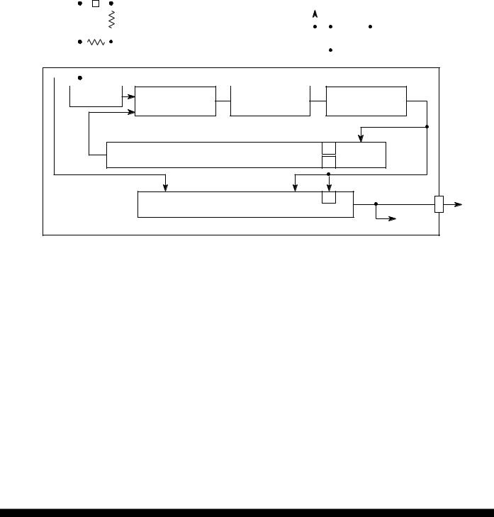
3.3 System Clock
The system clock in the SIM provides timing signals for the IMB modules and for an external peripheral bus. Because MCU operation is fully static, register and memory contents are not affected when the clock rate changes. System hardware and software support changes in the clock rate during operation.
The system clock signal can be generated in three ways. An internal phase-locked loop can synthesize the clock from an internal or external frequency source, or the clock signal can be input from an external source.
Following is a block diagram of the clock submodule.
|
|
|
|
|
|
|
|
|
|
|
|
|
|
|
|
|
|
|
|
|
|
|
|
|
|
|
|
|
|
|
VDDSYN |
|
|
|
|
|
|
|
|
|
|
|
|||
|
|
|
|
|
|
|
|
|
|
|
|
|
|
|
|
|
|
|
|
|
|
|
|
|
|
|
|
|
|
|
|
|
|
|
|
|
|
|
|
|
|
||||
22 pF |
2 |
|
|
|
|
|
|
|
|
|
|
|
|
|
|
|
|
|
|
|
|
|
|
22 pF |
2 |
|
|
|
XFC1 |
|
|
|
0.1µF |
||||||||||||
|
|
|
|
|
|
|
|
|
|
330k |
|
|
|
|
|
|
|
|
|
|
|
|
|
|
|||||||||||||||||||||
|
|
|
|
|
|
|
|
|
|
|
|
|
|
|
|
|
|
|
|
|
|
||||||||||||||||||||||||
|
|
|
|
|
|
|
|
|
|
|
|
10M |
|
|
|
|
|
|
|
|
|
|
|
|
|
|
|
|
|
|
|
|
|
|
|
|
|
|
|
|
|
|
|||
|
|
|
|
|
|
|
|
|
|
|
|
|
|
|
|
|
|
|
|
|
|
|
|
|
|
|
|
|
|
|
|
|
|
|
|
|
|
|
|
|
|
||||
VSSI |
|
|
|
|
|
|
|
|
|
|
|
|
|
|
|
|
|
VSSI |
|
|
|
|
0.1µF |
|
.01µF |
|
|
|
|
|
|
VSSI |
|||||||||||||
|
|
|
|
|
|
|
|
|
|
|
|
|
|
|
|
|
|
|
|
|
|
|
|
|
|
|
|
|
|
|
|
||||||||||||||
|
|
|
|
|
|
|
|
|
|
|
|
|
|
|
|
|
|
|
|
|
|
|
|
|
|
|
|
|
|
||||||||||||||||
|
EXTAL |
|
|
|
|
|
|
|
|
XTAL |
|
XFC PIN |
|
|
|
VDDSYN |
|
|
|
|
|
|
|
|
|
|
|
||||||||||||||||||
|
|
|
|
|
|
|
|
|
|
|
|
|
|
|
|
|
|
|
|
|
|
|
|
||||||||||||||||||||||
|
|
|
|
|
|
|
|
|
|
|
|
|
|
|
|
|
|
|
|
|
|
|
|
|
|||||||||||||||||||||
|
|
|
|
|
|
|
|
|
|
|
|
|
|
|
|
|
|
|
|
|
|
|
|
||||||||||||||||||||||
|
|
|
|
|
|
|
|
|
|
|
|
|
|
|
|
|
|
|
|
|
|
|
|
|
|
|
|
|
|
|
|
|
|
|
|
|
|
|
|
|
|
|
|
|
|
|
|
|
|
|
|
|
|
|
|
|
|
|
|
|
|
|
|
|
|
|
|
|
|
|
|
|
|
|
|
|
|
|
|
|
|
|
|
|
|
|
|
|
|
|
|
CRYSTAL |
PHASE |
LOW-PASS |
|
|
OSCILLATOR |
VCO |
|||
COMPARATOR |
FILTER |
|||
|
|
|||
|
|
W |
|
|
|
|
FEEDBACK DIVIDER |
|
|
|
|
Y |
|
|
|
|
X |
CLKOUT |
|
|
|
SYSTEM CLOCK CONTROL |
|
|
|
|
|
SYSTEM |
|
|
|
|
CLOCK |
1.MUST BE LOW-LEAKAGE CAPACITOR (INSULATION RESISTANCE 30,000 MΩ OR GREATER).
2.RESISTANCE AND CAPACITANCE BASED ON A TEST CIRCUIT CONSTRUCTED WITH A DAISHINKU DMX-38 32.768-kHz CRYSTAL. SPECIFIC COMPONENTS MUST BE BASED ON CRYSTAL TYPE. CONTACT CRYSTAL VENDOR FOR EXACT CIRCUIT.
SYS CLOCK
BLOCK 32KHZ
Figure 7 System Clock Block Diagram
3.3.1 Clock Sources
The state of the clock mode (MODCLK) pin during reset determines the clock source. When MODCLK is held high during reset, the clock synthesizer generates a clock signal from either a crystal oscillator or an external reference input. Clock synthesizer control register SYNCR determines operating frequency and various modes of operation. When MODCLK is held low during reset, the clock synthesizer is disabled, and an external system clock signal must be applied. When the synthesizer is disabled, SYNCR control bits have no effect.
A reference crystal must be connected between the EXTAL and XTAL pins to use the internal oscillator. Use of a 32.768-kHz crystal is recommended. These crystals are inexpensive and readily available. If an external reference signal or an external system clock signal is applied through the EXTAL pin, the XTAL pin must be left floating. External reference signal frequency must be less than or equal to maximum specified reference frequency. External system clock signal frequency must be less than or equal to maximum specified system clock frequency.
MC68332 |
MOTOROLA |
MC68332TS/D |
23 |

When an external system clock signal is applied (i.e., the PLL is not used), duty cycle of the input is critical, especially at near maximum operating frequencies. The relationship between clock signal duty cycle and clock signal period is expressed:
Minimum external clock period =
minimum external clock high/low time
50% — percentage variation of external clock input duty cycle
3.3.2 Clock Synthesizer Operation
A voltage controlled oscillator (VCO) generates the system clock signal. A portion of the clock signal is fed back to a divider/counter. The divider controls the frequency of one input to a phase comparator. The other phase comparator input is a reference signal, either from the internal oscillator or from an external source. The comparator generates a control signal proportional to the difference in phase between its two inputs. The signal is low-pass filtered and used to correct VCO output frequency.
The synthesizer locks when VCO frequency is identical to reference frequency. Lock time is affected by the filter time constant and by the amount of difference between the two comparator inputs. Whenever comparator input changes, the synthesizer must re-lock. Lock status is shown by the SLOCK bit in SYNCR.
The MCU does not come out of reset state until the synthesizer locks. Crystal type, characteristic frequency, and layout of external oscillator circuitry affect lock time.
The low-pass filter requires an external low-leakage capacitor, typically 0.1 F, connected between the XFC and VDDSYN pins.
VDDSYN is used to power the clock circuits. A separate power source increases MCU noise immunity and can be used to run the clock when the MCU is powered down. Use a quiet power supply as the VDDSYN source, since PLL stability depends on the VCO, which uses this supply. Place adequate external bypass capacitors as close as possible to the VDDSYN pin to ensure stable operating frequency.
When the clock synthesizer is used, control register SYNCR determines operating frequency and various modes of operation. SYNCR can be read only when the processor is operating at the supervisor privilege level.
The SYNCR X bit controls a divide by two prescaler that is not in the synthesizer feedback loop. Setting X doubles clock speed without changing VCO speed. There is no VCO relock delay. The SYNCR W bit controls a 3-bit prescaler in the feedback divider. Setting W increases VCO speed by a factor of four. The SYNCR Y field determines the count modulus for a modulo 64 down counter, causing it to divide by a value of Y + 1. When either W or Y value changes, there is a VCO relock delay.
Clock frequency is determined by SYNCR bit settings as follows:
FSYSTEM = FREFERENCE [4(Y + 1)(22W + X)]
In order for the device to perform correctly, the clock frequency selected by the W, X, and Y bits must be within the limits specified for the MCU.
The VCO frequency is twice the system clock frequency if X = 1 or four times the system clock frequency if X = 0.
The reset state of SYNCR ($3F00) produces a modulus-64 count.
MOTOROLA |
MC68332 |
24 |
MC68332TS/D |

3.3.3 Clock Control
The clock control circuits determine system clock frequency and clock operation under special circumstances, such as following loss of synthesizer reference or during low-power operation. Clock source is determined by the logic state of the MODCLK pin during reset.
SYNCR —Clock Synthesizer Control Register |
|
|
|
|
|
|
|
$YFFA04 |
|||||||
15 |
14 |
13 |
|
|
|
|
8 |
7 |
6 |
5 |
4 |
3 |
2 |
1 |
0 |
|
|
|
|
|
|
|
|
|
|
|
|
|
|
|
|
W |
X |
|
|
|
Y |
|
|
EDIV |
0 |
0 |
SLIMP |
SLOCK |
RSTEN |
STSIM |
STEXT |
|
|
|
|
|
|
|
|
|
|
|
|
|
|
|
|
RESET: |
|
|
|
|
|
|
|
|
|
|
|
|
|
|
|
0 |
0 |
1 |
1 |
1 |
1 |
1 |
1 |
0 |
0 |
0 |
U |
U |
0 |
0 |
0 |
When the on-chip clock synthesizer is used, system clock frequency is controlled by the bits in the upper byte of SYNCR. Bits in the lower byte show status of or control operation of internal and external clocks. The SYNCR can be read or written only when the CPU is operating at the supervisor privilege level.
W — Frequency Control (VCO)
This bit controls a prescaler tap in the synthesizer feedback loop. Setting the bit increases the VCO speed by a factor of four. VCO relock delay is required.
X — Frequency Control Bit (Prescale)
This bit controls a divide by two prescaler that is not in the synthesizer feedback loop. Setting the bit doubles clock speed without changing the VCO speed. There is no VCO relock delay.
Y[5:0] — Frequency Control (Counter)
The Y field controls the modulus down counter in the synthesizer feedback loop, causing it to divide by a value of Y + 1. Values range from 0 to 63. VCO relock delay is required.
EDIV — E Clock Divide Rate
0 = ECLK frequency is system clock divided by 8. 1 = ECLK frequency is system clock divided by 16.
ECLK is an external M6800 bus clock available on pin ADDR23. Refer to 3.5 Chip Selects for more information.
SLIMP — Limp Mode Flag
0 = External crystal is VCO reference.
1 = Loss of crystal reference.
When the on-chip synthesizer is used, loss of reference frequency causes SLIMP to be set. The VCO continues to run using the base control voltage. Maximum limp frequency is maximum specified system clock frequency. X-bit state affects limp frequency.
SLOCK — Synthesizer Lock Flag
0 = VCO is enabled, but has not locked.
1 = VCO has locked on the desired frequency (or system clock is external).
The MCU maintains reset state until the synthesizer locks, but SLOCK does not indicate synthesizer lock status until after the user writes to SYNCR.
RSTEN — Reset Enable
0 = Loss of crystal causes the MCU to operate in limp mode. 1 = Loss of crystal causes system reset.
STSIM — Stop Mode SIM Clock
0 = When LPSTOP is executed, the SIM clock is driven from the crystal oscillator and the VCO is turned off to conserve power.
1 = When LPSTOP is executed, the SIM clock is driven from the VCO.
STEXT — Stop Mode External Clock
0 = When LPSTOP is executed, the CLKOUT signal is held negated to conserve power.
1 = When LPSTOP is executed, the CLKOUT signal is driven from the SIM clock, as determined by the state of the STSIM bit.
MC68332 |
MOTOROLA |
MC68332TS/D |
25 |

3.4 External Bus Interface
The external bus interface (EBI) transfers information between the internal MCU bus and external devices. The external bus has 24 address lines and 16 data lines.
The EBI provides dynamic sizing between 8-bit and 16-bit data accesses. It supports byte, word, and long-word transfers. Ports are accessed through the use of asynchronous cycles controlled by the data transfer (SIZ1 and SIZ0) and data size acknowledge pins (DSACK1 and DSACK0). Multiple bus cycles may be required for a transfer to or from an 8-bit port.
Port width is the maximum number of bits accepted or provided during a bus transfer. External devices must follow the handshake protocol described below. Control signals indicate the beginning of the cycle, the address space, the size of the transfer, and the type of cycle. The selected device controls the length of the cycle. Strobe signals, one for the address bus and another for the data bus, indicate the validity of an address and provide timing information for data. The EBI operates in an asynchronous mode for any port width.
To add flexibility and minimize the necessity for external logic, MCU chip-select logic can be synchronized with EBI transfers. Chip-select logic can also provide internally-generated bus control signals for these accesses. Refer to 3.5 Chip Selects for more information.
3.4.1 Bus Control Signals
The CPU initiates a bus cycle by driving the address, size, function code, and read/write outputs. At the beginning of the cycle, size signals SIZ0 and SIZ1 are driven along with the function code signals. The size signals indicate the number of bytes remaining to be transferred during an operand cycle. They are valid while the address strobe (AS) is asserted. The following table shows SIZ0 and SIZ1 encoding. The read/write (R/W) signal determines the direction of the transfer during a bus cycle. This signal changes state, when required, at the beginning of a bus cycle, and is valid while AS is asserted. R/W only changes state when a write cycle is preceded by a read cycle or vice versa. The signal can remain low for two consecutive write cycles.
Table 8 Size Signal Encoding
SIZ1 |
SIZ0 |
Transfer Size |
|
|
|
0 |
1 |
Byte |
|
|
|
1 |
0 |
Word |
|
|
|
1 |
1 |
Three Byte |
|
|
|
0 |
0 |
Long Word |
|
|
|
3.4.2 Function Codes
The CPU32 automatically generates function code signals FC[2:0]. The function codes can be considered address extensions that automatically select one of eight address spaces to which an address applies. These spaces are designated as either user or supervisor, and program or data spaces. Address space 7 is designated CPU space. CPU space is used for control information not normally associated with read or write bus cycles. Function codes are valid while AS is asserted.
MOTOROLA |
MC68332 |
26 |
MC68332TS/D |

Table 9 CPU32 Address Space Encoding
FC2 |
FC1 |
FC0 |
Address Space |
|
|
|
|
0 |
0 |
0 |
Reserved |
|
|
|
|
0 |
0 |
1 |
User Data Space |
|
|
|
|
0 |
1 |
0 |
User Program Space |
|
|
|
|
0 |
1 |
1 |
Reserved |
|
|
|
|
1 |
0 |
0 |
Reserved |
|
|
|
|
1 |
0 |
1 |
Supervisor Data Space |
|
|
|
|
1 |
1 |
0 |
Supervisor Program Space |
|
|
|
|
1 |
1 |
1 |
CPU Space |
|
|
|
|
3.4.3 Address Bus
Address bus signals ADDR[23:0] define the address of the most significant byte to be transferred during a bus cycle. The MCU places the address on the bus at the beginning of a bus cycle. The address is valid while AS is asserted.
3.4.4 Address Strobe
AS is a timing signal that indicates the validity of an address on the address bus and the validity of many control signals. It is asserted one-half clock after the beginning of a bus cycle.
3.4.5 Data Bus
Data bus signals DATA[15:0] make up a bidirectional, non-multiplexed parallel bus that transfers data to or from the MCU. A read or write operation can transfer 8 or 16 bits of data in one bus cycle. During a read cycle, the data is latched by the MCU on the last falling edge of the clock for that bus cycle. For a write cycle, all 16 bits of the data bus are driven, regardless of the port width or operand size. The MCU places the data on the data bus one-half clock cycle after AS is asserted in a write cycle.
3.4.6 Data Strobe
Data strobe (DS) is a timing signal. For a read cycle, the MCU asserts DS to signal an external device to place data on the bus. DS is asserted at the same time as AS during a read cycle. For a write cycle, DS signals an external device that data on the bus is valid. The MCU asserts DS one full clock cycle after the assertion of AS during a write cycle.
3.4.7 Bus Cycle Termination Signals
During bus cycles, external devices assert the data transfer and size acknowledge signals (DSACK1 and DSACK0). During a read cycle, the signals tell the MCU to terminate the bus cycle and to latch data. During a write cycle, the signals indicate that an external device has successfully stored data and that the cycle can end. These signals also indicate to the MCU the size of the port for the bus cycle just completed. (Refer to 3.4.9 Dynamic Bus Sizing.)
The bus error (BERR) signal is also a bus cycle termination indicator and can be used in the absence of DSACK1 and DSACK0 to indicate a bus error condition. It can also be asserted in conjunction with these signals, provided it meets the appropriate timing requirements. The internal bus monitor can be used to generate the BERR signal for internal and internal-to-external transfers. When BERR and HALT are asserted simultaneously, the CPU takes a bus error exception.
Autovector signal (AVEC) can terminate external IRQ pin interrupt acknowledge cycles. AVEC indicates that the MCU will internally generate a vector number to locate an interrupt handler routine. If it is continuously asserted, autovectors will be generated for all external interrupt requests. AVEC is ignored during all other bus cycles.
MC68332 |
MOTOROLA |
MC68332TS/D |
27 |
Loading...