


|
|
|
Order this document by MC44353/D |
|
|
|
|
MC44353 |
|
Advance Information |
MC44354 |
|||
PLL |
Tuned |
UHF Audio/Video |
MC44355 |
|
|
||||
Modulator ICs for PAL, SECAM |
|
|||
and |
NTSC |
TV Systems |
MULTI±STANDARD |
|
MC44353 ± Multi±Standard Modulator IC |
||||
AND PAL/NTSC |
||||
MC44354 ± PAL/NTSC Modulator IC |
||||
MODULATOR ICs |
||||
MC44355 ± PAL/NTSC Modulator IC with |
||||
|
||||
|
Fixed Video Modulation Index |
SEMICONDUCTOR |
||
|
|
|
||
These modulator circuits are intended for use in VCRs, satellite receivers, |
TECHNICAL DATA |
|||
set±top boxes, video games, etc. An on±chip high speed I2C compatible bus |
|
|||
receiver is included and is used to set the channel, tuned by a PLL over the |
|
|||
full range in the UHF bands. The modulator incorporates a sound subcarrier |
|
|||
oscillator, using a second PLL to derive 4.5, 5.5, 6.0 and 6.5 MHz carrier |
|
|||
frequencies, selectable by the bus. |
|
|||
For the sound, either frequency modulation with pre±emphasis or |
20 |
|||
amplitude modulation (MC44353 only) is possible. A control bit (MC44353 |
1 |
|||
only) is used to select AM sound with positive RF modulation (system L). The |
||||
DTB SUFFIX |
||||
level of the sound carrier with respect to the vision carrier and the modulation |
||||
depth of both sound and vision may be adjusted by means of the bus. In |
PLASTIC PACKAGE |
|||
CASE 948E |
||||
addition, an on±chip video test pattern generator may be switched in with a |
||||
(TSSOP±20) |
||||
|
|
|
||
1.0kHz audio test signal.
•Channel 21 through 69 UHF Operation (471 MHz to 855 MHz)
•On±Chip Low Power Operational Amplifier for Direct Tuning Varactor Voltage
• Single±Ended Output for Low Cost and Ease of Interface |
20 |
|
|
|
|||
• Low External Component Count |
|
|
|
1 |
|
||
• High Speed I2C Bus Compatible |
|
|
|
|
|||
|
|
|
|
|
|||
• Programmable Video Modulation Depth (8 Steps of 2.5%) |
|
DW SUFFIX |
|
||||
• Programmable Picture/Sound Carriers Ratio and Audio Sensitivity |
PLASTIC PACKAGE |
||||||
|
CASE 751D |
|
|||||
(8 Steps of 1.0 dB) |
|
|
|
|
(SO±20L) |
|
|
• On±Chip Programmable Sound Subcarrier Oscillator (4.5 MHz to |
|
|
|
|
|||
6.5 MHz) |
|
|
|
|
|
|
|
• On±Chip Video Test Pattern Generator with Sound Test Signal (1.0 kHz) |
|
|
|
|
|||
• VCC Standby Mode (Typ 500 μA) |
|
PIN CONNECTIONS |
|||||
• Transient Output Inhibit During PLL Lock±Up at Power±On |
|||||||
|
|
|
|
||||
|
|
|
Amp In |
1 |
20 |
Xtal |
|
|
|
|
Op Out |
2 |
19 |
SDA |
|
|
ORDERING INFORMATION |
|
VCCD |
3 |
18 |
SCL |
|
|
Operating |
|
Osc Gnd |
4 |
17 |
Mod Gnd |
|
|
|
Osc |
5 |
16 |
VCC Mod |
||
Device |
Temperature Range |
Package |
|||||
MC44353DTB |
|
TSSOP±20 |
Osc |
6 |
15 |
RF Out |
|
|
Osc Gnd |
7 |
14 |
Mod Gnd |
|||
|
|
|
|||||
MC44353DW |
|
SO±20L |
Snd Fil |
8 |
13 |
Video In |
|
MC44354DTB |
TA = ±20° to +80°C |
TSSOP±20 |
Snd Tun |
9 |
12 |
VCCA |
|
MC44354DW |
SO±20L |
Pre±Em |
10 |
11 |
Audio In |
||
|
|
|
|
|
|||
MC44355DTB |
|
TSSOP±20 |
|
|
(Top View) |
|
|
MC44355DW |
|
SO±20L |
|
|
|
|
|
This document contains information on a new product. Specifications and information herein |
Motorola, Inc. 1998 |
|
|
Rev 0 |
|||
are subject to change without notice.

MC44353 MC44354 MC44355
Figure 1. MC44353 Simplified Block Diagram
|
|
VCCA |
Mod Gnd |
|
Video In |
|
|
Snd Fil |
Snd Tun |
||
|
|
12 |
14 |
|
|
13 |
|
|
8 |
|
9 |
VCC Mod Standby |
16 |
|
Peak |
|
|
|
|
Phase/ |
|
|
|
|
|
|
Clamp |
|
|
|
|
||||
|
|
|
White Clip |
|
|
Freq Comp |
|
|
|
||
|
|
|
|
|
|
|
|
|
|
||
|
15 |
|
|
|
|
|
|
|
Sound Osc |
10 |
|
RF Out |
|
|
MC44353 |
2 |
|
+ FM Mod |
Pre±Em |
||||
|
|
|
Prog Divider |
||||||||
|
|
Video |
|
||||||||
|
|
|
|
|
|
|
|
|
|
||
|
|
|
|
|
|
|
|
|
|
3 |
|
|
|
|
Modulator |
|
|
|
|
|
|
|
|
|
|
8 |
+ Sound Mix |
|
|
3 |
AM Mod |
|
|
11 |
|
|
17 |
|
|
|
|
|
|
|
|
|
Audio |
Mod Gnd |
|
|
|
|
|
|
|
|
|
|
|
|
|
Test Pattern |
|
|
|
|
|
|
7 |
||
|
|
|
|
|
|
|
|
|
|||
|
|
30 |
|
|
|
|
|
|
Osc Gnd |
||
|
|
Generator |
|
|
|
|
|
|
|||
|
18 |
|
|
|
|
UHF |
|
6 |
|||
SCL |
|
|
|
|
|
|
|
|
|||
|
High |
TE1 |
TE2 |
|
|
|
|
|
Osc |
||
|
|
7.8 kHz |
|
|
Osc |
|
|||||
|
19 |
|
|
|
|
5 |
|||||
SDA |
Speed Bus |
|
|
|
|
|
|
and |
|
||
|
|
|
|
|
976 Hz |
|
|
Drives |
|
Osc |
|
|
|
Modulator |
|
|
|
|
|
|
|
4 |
|
|
|
|
|
|
|
|
|
|
|
||
|
|
|
|
|
|
|
|
|
|
Osc Gnd |
|
|
|
Section |
|
|
|
|
|
|
|
|
|
|
|
|
|
|
|
|
|
|
|
|
|
|
|
PLL |
|
|
|
|
|
8 |
|
|
|
|
|
|
|
12 |
Prog |
|
Prescaler |
|
|
|
|
|
|
Section |
|
|
|
|
|
3 |
|
|
|
|
|
|
|
|
Divider |
|
|
|
|||
|
|
|
|
|
|
Phase |
|
|
|
||
|
20 |
|
|
|
|
|
|
Bias |
|
|
|
Xtal |
Ref Osc |
Ref Divider |
|
31.25 kHz |
Comp |
|
2 |
||||
|
|
|
|
||||||||
|
|
|
|
|
|||||||
Op Out
|
|
|
|
3 |
1 |
|
|
|
|
||||
MAXIMUM RATINGS (Note 1) |
|
VCCD |
Amp In |
|||
|
|
|
|
|
|
|
|
|
|
|
|
|
|
Rating |
Symbol |
|
|
Value |
Unit |
|
|
|
|
|
|
||
Supply Voltage |
VCC |
7 |
V |
|
||
Operational Amplifier Output Voltage |
|
36 |
V |
|
||
|
|
|
|
|
|
|
Operating Ambient Temperature |
TA |
|
|
±20 to 80 |
°C |
|
Storage Temperature |
Tstg |
|
|
±65 to 150 |
°C |
|
NOTES: 1. Maximum ratings are those values beyond which damage to the device may occur. For functional operation, voltages should be restricted to the Recommended Operating Conditions.
2. ESD data available upon request.
ELECTRICAL CHARACTERISTICS (Parameter Type: A±100% Tested, B±100% Correlation Tested, C±Characterized on Samples. D±Design Parameter, VCC = 5.0 V, TA = 25C, Video input 1.0 Vpp, 10 step greyscale. Step 3 [typ. 80%] modulation depth for PAL; Step 5 [typ 90%] modulation for SECAM L; P/S ration Step 3 [typ 14.5 dB]. RF output into 75 Ω load. Unless otherwise noted.) (Specifications only valid for envelope demodulation.)
Characteristic |
Symbol |
Min |
Typ |
Max |
Unit |
Type |
|
|
|
|
|
|
|
Operating Supply Voltage Range |
VCCA,VCCD, |
4.5 |
5.0 |
5.5 |
V |
D |
|
VCC Mod |
|
|
|
|
|
Analog Section Supply Current (VCC = 5.0 V) |
ICCA |
26 |
33 |
39.5 |
mA |
A |
Digital Section Supply Current (VCC = 5.0 V) |
ICCD |
24 |
32 |
39 |
mA |
A |
Modulator O/P Section Supply Current (VCC = 5.0 V) |
ICC Mod |
6.0 |
9.0 |
11.5 |
mA |
A |
Total Supply Current (VCC = 5.0 V) |
ICC |
56 |
74 |
90 |
mA |
A |
During Standby |
VCC Mod |
4.0 |
± |
5.5 |
V |
D |
During Standby (with Data Retension: VCC Mod = 5.0V) |
ICC Mod |
± |
0.5 |
1.0 |
mA |
B |
Operational Amplifier Output Voltage (through Rpullup) |
|
± |
30 |
35 |
V |
B |
Operational Amplifier Output Current (with Rpullup = 560 kΩ |
|
± |
56 |
100 |
μA |
B |
|
|
|
|
|
|
|
Test Pattern Sync Pulse Width |
TE1 |
4.0 |
4.7 |
5.6 |
μs |
A |
2 |
MOTOROLA ANALOG IC DEVICE DATA |
MC44353 MC44354 MC44355
ELECTRICAL CHARACTERISTICS (continued) (Parameter Type: A±100% Tested, B±100% Correlation Tested, C±Characterized on Samples. D±Design Parameter, VCC = 5.0 V, TA = 25C, Video input 1.0 Vpp, 10 step greyscale. Step 3 [typ. 80%] modulation depth for PAL; Step 5 [typ 90%] modulation for SECAM L; P/S ration Step 3 [typ 14.5 dB]. RF output into 75 Ω load. Unless otherwise noted.) (Specifications only valid for envelope demodulation.)
Characteristic |
Symbol |
Min |
Typ |
Max |
Unit |
Type |
|
|
|
|
|
|
|
UHF Comparator Pump Current (Note 1) |
|
2.0 |
4.0 |
6.0 |
μA |
A |
|
|
|
|
|
|
|
Sound Comparator Pump Current (Note 2) |
|
2.0 |
3.8 |
5.6 |
μA |
A |
|
|
|
|
|
|
|
Op±Amp Input Current |
|
± |
± |
20 |
nA |
A |
|
|
|
|
|
|
|
Oscillator Stability ± negative resistance |
|
1.0 |
± |
± |
kΩ |
D |
|
|
|
|
|
|
|
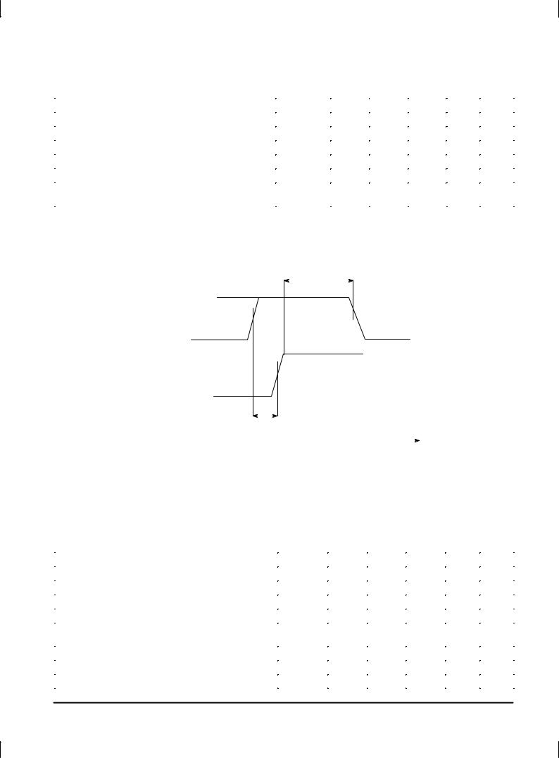
Delay VCCA/D to VCC Mod Application (See Figure 2) |
t_sup_del |
0 |
± |
± |
ns |
D |
VCCA/D & VCC Mod Duration for Standby Mode Function |
t_sup_min |
30 |
± |
± |
ms |
D |
(See Figure 2) |
|
|
|
|
|
|
|
|
|
|
|
|
|
NOTES: 1. Current sources driven by the UHF phase comparactor, that are connected to Pin 1. 2. Current sources driven by the phase sound comparator, that are connected to Pin 8.
Figure 2. Initial Power±On and Standby Mode VCC Timing Diagram
|
|
|
|
|
|
|
t_sup_min |
|
|
|
|
|
|
|
|
|
|
|
|
|
5.0 V |
|
|
|
|
|
|
|
|
|
|
|
|||
|
|
|
|
|
|
|
|
|
|
|
|
|
|
||||
VCCA/D |
0 V |
|
|
|
|
|
|
|
0 V |
|
|
||||||
VCCmod |
0 V |
|
|
|
|
|
|
|
|
|
|
|
5.0 V |
|
|
||
|
|
|
|
|
|
|
|
|
|
|
|
|
|||||
|
|
|
|
|
|
|
|
|
|
|
|
|
|
|
|||
|
|
|
|
|
|
|
|
|
|
|
|
||||||
|
|
|
|
|
|
|
|
|
|
|
|
|
|
|
|
|
|
|
|
|
|
t_sup_del |
|
|
|
|
|
|
|
|
|
|
|
||
|
|
|
|
|
|
|
|
|
|
|
|
|
|
|
|
|
|
|
|
|
|
|
|
|
|
|
|
|
|
|
|
time |
|
|
|
For proper operation of internal reset functions, VCCA and |
VCCmodisnotappliedbeforeVCCAandVCCD(whichmustbe |
||||||||||||||||
VCCD (which must be applied simultaneously) may not be |
tied together). See the timing diagram and DATA |
||||||||||||||||
applied after VCCmod. |
|
|
|
|
|
|
RETENTION function description. |
|
|
||||||||
Normally, all VCC lines will come up at the same time. |
NotethatVCCA/DandVCCmodmustbeactivatedabove4.5 |
||||||||||||||||
However, due to the possibility of a Standby VCC to be |
V for a least 30 msecs before the device can operate |
||||||||||||||||
applied to the VCCmod pin, care should be ensured that |
correctly in Standby Mode. |
|
|
|
|
||||||||||||
HIGH SPEED I2C COMPATIBLE BUS CHARACTERISTICS (Over Functional Temperature Range ± V = 5.0 V) |
|
||||||||||||||||
|
|
|
|
|
|
|
|
|
|
|
|
|
|
CC |
|
|
|
Characteristic |
|
Symbol |
|
Min |
|
Typ |
|
Max |
Unit |
Type |
|||||||
|
|
|
|
|
|
|
|
|
|
|
|
|
|
|
|
|
|
SDA/SCL Output Current at 0 V |
|
|
|
|
|
|
|
|
± |
|
|
± |
|
10 |
μA |
A |
|
|
|
|
|
|
|
|
|
|
|
|
|
|
|
|
|
|
|
SDA/SCL Low Input Level |
|
|
|
|
|
|
Vil |
|
± |
|
|
± |
|
1.5 |
V |
B |
|
SDA/SCL High Input Level |
|
|
|
|
|
|
Vih |
|
3.0 |
|
± |
|
± |
V |
B |
||
SDA/SCL Input Current for Input Level from 0.4 V to 0.3 VCC |
|
|
|
±5.0 |
|
± |
|
5.0 |
μA |
C |
|||||||
SDA/SCL Input Level |
|
|
|
|
|
|
|
|
0 |
|
|
± |
|
VCC |
V |
D |
|
|
|
|
|
|
|
|
|
|
|
|
|
|
|
+ 0.3 |
|
|
|
|
|
|
|
|
|
|
|
|
|
|
|
|
|
|
|
|
|
SDA/SCL Capacitance |
|
|
|
|
|
|
Ci |
|
± |
|
|
± |
|
10 |
pF |
C |
|
ACK Low Output Level (sinking 3.0 mA) |
|
|
|
± |
|
|
0.3 |
|
1.0 |
V |
A |
||||||
|
|
|
|
|
|
|
|
|
|
|
|
||||||
ACK Low Output Level (sinking 15 mA) |
|
|
|
± |
|
|
± |
|
1.5 |
V |
C |
||||||
|
|
|
|
|
|
|
|
|
|
|
|
|
|
|
|
|
|
MOTOROLA ANALOG IC DEVICE DATA |
3 |
|

MC44353 MC44354 MC44355
HIGH SPEED I2C COMPATIBLE BUS CHARACTERISTICS (continued) (Over Functional Temperature Range ± V |
= 5.0 V) |
||||||
|
|
|
|
|
CC |
|
|
Characteristic |
Symbol |
Min |
Typ |
Max |
Unit |
|
Type |
|
|
|
|
|
|
|
|
Bus Clock Frequency |
|
0 |
± |
800 |
kHz |
|
C |
|
|
|
|
|
|
|
|
Bus Free Time Between Stop and Start |
Tbuf |
200 |
± |
± |
ns |
|
C |
Setup Time for Start Conditions |
Tsu;sta |
500 |
± |
± |
ns |
|
C |
Hold Time for Start Condition |
Thd;sta |
500 |
± |
± |
ns |
|
C |
Data Setup Time |
Tsu;dat |
0 |
± |
± |
ns |
|
C |
Data Hold Time |
Thd;dat |
0 |
± |
± |
ns |
|
C |
Setup Time for Stop Condition |
Tsu;sto |
500 |
± |
± |
ns |
|
C |
Hold time for Stop Condition |
Thd;sto |
500 |
± |
± |
ns |
|
C |
Acknowledge Propagation Delay |
Tack;low |
± |
± |
300 |
ns |
|
C |
SDA Fall Time at 3.0 mA sink and 130 pF Load |
|
± |
± |
50 |
ns |
|
C |
|
|
|
|
|
|
|
|
SDA Fall Time at 3.0 mA sink and 400 pF Load |
|
± |
± |
80 |
ns |
|
C |
|
|
|
|
|
|
|
|
SDA/SCL Rise Time |
|
± |
± |
300 |
ns |
|
C |
|
|
|
|
|
|
|
|
SCL Fall Time |
|
± |
± |
300 |
ns |
|
C |
|
|
|
|
|
|
|
|
Pulse Width of Spikes Suppressed by the Input Filter |
Tsp |
± |
± |
50 |
ns |
|
C |
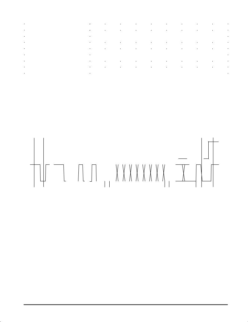
Figure 3. Timings Definition
Tbuf
Stop |
Start |
Chip address |
ACK |
SDA
SCL
Tsu;sto Thd;sta |
|
Tsu;dat Thd;dat |
Tack:low |
|
Start |
Stop |
|
SDA |
SDA |
|
|
|
|
||
SCL |
|
SCL |
|
Tsu;sta |
|
|
Thd;sto |
Figure 4. Levels Definition
VCC
VIH
Not Defined
VIL
0 V
4 |
MOTOROLA ANALOG IC DEVICE DATA |
MC44353 MC44354 MC44355
High Speed I2C Compatible Bus Format
|
|
Bit 7 |
|
|
|
|
|
|
Bit 0 |
ACK |
|
|
|
|
|
|
|
|
|
|
|
CA ± Chip Address |
1 |
1 |
0 |
0 |
1 |
0 |
1 |
0 |
ACK |
|
|
|
|
|
|
|
|
|
|
|
|
|
|
|
|
|
|
|
|
|
|
|
C0 |
± Low Order Bits |
VMD2 |
VMD1 |
VMD0 |
SFD1 |
SFD0 |
TB2 |
TB1 |
TB0 |
ACK |
|
|
|
|
|
|
|
|
|
|
|
C1 |
± High Order Bits |
1 |
AMD2 |
AMD1 |
AMD0 |
PSD2 |
PSD1 |
PSD0 |
SysL |
ACK |
|
|
|
|
|
|
|
|
|
|
|
|
|
|
|
|
|
|
|
|
|
|
FL ± Low Order Bits |
N5 |
N4 |
N3 |
N2 |
N1 |
N0 |
X1 |
X0 |
ACK |
|
FM ± High Order Bits |
0 |
TPEN |
N11 |
N10 |
N9 |
N8 |
N7 |
N6 |
ACK |
|
NOTES: 1. C0 and FL: Low Order Bits and C1 and FM: High Order Bits.
2.VDM0±2: Video Mod Depth control bits (for MC44355 VMD0±2 are Don't Care).
3.SFD0±1: Sound subcarrier frequency control bits.
4.TB0±2 and X1, X0: Test modes bits, see table entitled TEST MODES.
5.AMD0±2: Audio Modulation Sensitivity, see table entitled AUDIO MODULATION SENSITIVITY (for MC44355 AMD0±2 are Don't Care).
6.PSD0±2: Picture to Sound carrier ratio, see table entitled PICTURE to SOUND CARRIER RATIO (for MC44355 PSD0±1 are Don't Care).
7.SysL: System L enable (selects AM sound and positive video modulation, MC44353 only).
8.TPEN: Test pattern enable (picture and sound).
9.N0 to N11: UHF frequency programming bits, in steps of 250 kHz.
Figure 5. High Speed I2C Compatible bus data format
SCL
|
|
|
1 |
2 |
3 |
4 |
5 |
6 |
7 |
8 |
9 |
10 |
11 |
12 |
13 |
|
14 |
15 |
16 |
17 |
18 |
|
19 |
|
|
|
|
|
|
44 |
45 |
|
|||||||||||||||||||||
|
|
|
|
|
|
|
|
|
|
|
|
|
|
|
|
|
|
|
|
|
|
|
|
|
|
|
|
|
|
|
|
|
|
|
|
|
|
|
|
|
|
|
|
|
|
|
|
|
|
|
|
|
|
|
|
|
|
|
|
|
|
|
|
|
|
|
|
|
|
|
|
|
|
|
|
|
|
|
|
|
|
|
|
|
|
|
|
|
|
|
|
|
|
|
|
|
|
|
|
|
|
|
|
|
|
|
|
|
|
|
|
|
|
|
|
|
|
|
|
|
|
|
|
|
|
|
|
|
|
|
|
|
|
|
|
|
|
|
|
|
|
|
|
|
|
|
|
|
|
|
|
|
|
|
|
|
|
|
|
|
|
STA |
Chip Address ($CA) |
First Data Byte (C1 or FM) |
Data |
STO |
|
ACK |
ACK |
|
ACK |
SDA |
|
|
|
|
MOTOROLA ANALOG IC DEVICE DATA |
5 |
|

MC44353 MC44354 MC44355
VIDEO CHARACTERISTICS
Characteristic |
Test Conditions |
Min |
Typ |
Max |
Unit |
Type |
|
|
|
|
|
|
|
|
|
Video Bandwidth |
(0/±1.0 dB; ref 0 dB @ 100 kHz) |
5 |
- |
± |
MHz |
C |
|
|
|
|
|
|
|
|
|
Video Input Level |
|
± |
± |
1.5 |
VCVBS |
D |
|
Video Input Current |
|
± |
50 |
200 |
nA |
A |
|
|
|
|
|
|
|
|
|
Peak White Clip (Note 1) |
|
108 |
112 |
116 |
% |
B |
|
|
|
|
|
|
|
|
|
Video Input Impedance |
Measured at 1.0 kHz (at Pin 13) |
± |
500/4 |
± |
kΩ/pF |
D |
|
|
|
|
|
|
|
|
|
Video S/N |
See Note 2 |
± |
Figure 6 |
Figure 6 |
dB |
C |
|
|
|
|
|
|
|
||
Differential Phase |
Figure 7 |
Figure 7 |
Figure 7 |
° |
C |
||
|
|||||||
|
|
|
|
|
|
|
|
Differentical Gain |
On line CCIR 310, worst from the |
± |
1.0 |
5 |
% |
C |
|
|
first 4 steps out of 5 |
|
|
|
|
|
|
|
|
|
|
|
|
|
|
Luma/Sync ratio |
Input ratio 7.0:3.0 |
6.8/3.2 |
± |
7.2/2.8 |
|
B |
|
|
|
|
|
|
|
|
|
PAL Video Modulation Depth Step 3 |
|
76 |
82 |
88 |
% |
B |
|
|
Programmable in 8 steps of 2.5% |
|
|
|
|
|
|
SECAM Video Modulation Depth |
84.5 |
90.5 |
96.5 |
% |
B |
||
Step 5 (MC44353 Only) |
|
|
|
|
|
|
|
|
|
|
|
|
|
|
NOTES: 1. The circuit is equipped with a 'soft clip' function. The Video Modulation depth is measured for a 1.0 VCVBS input level, giving modulation depth MDA; then the same measurement is carried out for an input level of 1.5 VCVBS, giving modulation depth MDB. The Peak White Clip is defined as 100*(MDB)/(MBA).
2.The frequency dependent specifications are greatly influenced by the PCB layout in the application. These specifications have all been measured using a Motorola application layout and circuit similarly as shown in Figures 19 and 21. The reference number for ordering this evaluation board is MC44350EVK.
Figure 6. Video Signal to Noise
60 |
|
|
|
|
|
|
|
|
|
|
|
|
|
|
|
|
|
|
|
|
|
|
Typical Performance |
|
|
|
|
|
|||||
55 |
|
|
|
|
|
|
|
|
|
|
|
|
|
|
|
|
dB |
|
|
|
|
|
|
|
|
|
|
|
|
|
|
|
|
50 |
|
|
|
|
Maximum Specification Limit |
|
|
|
|
|||||||
|
|
|
|
|
|
|
|
|
|
|
|
|
|
|
|
|
45 |
24 |
27 |
30 |
33 |
36 |
39 |
42 |
45 |
48 |
51 |
54 |
57 |
60 |
63 |
66 |
69 |
21 |
||||||||||||||||
|
|
|
|
|
|
Channel Number |
|
|
|
|
|
|
||||
Figure 7. Differential Phase
|
8.0 |
|
|
|
|
|
|
|
|
|
|
|
|
|
|
|
|
|
6.0 |
|
|
|
|
Maximum Specification Limit |
|
|
|
|
|||||||
|
4.0 |
|
|
|
|
|
|
|
|
|
|
|
|
|
|
|
|
Degrees |
2.0 |
|
|
|
|
|
|
|
|
|
|
|
|
|
|
|
|
0 |
|
|
|
|
|
Typical Performance |
|
|
|
|
|
||||||
|
|
|
|
|
|
|
|
|
|
|
|||||||
|
±2.0 |
|
|
|
|
|
|
|
|
|
|
|
|
|
|
|
|
|
±4.0 |
|
|
|
|
|
|
|
|
|
|
|
|
|
|
|
|
|
±6.0 |
|
|
|
|
|
Minimum Specification Limit |
|
|
|
|
|
|||||
|
±8.0 |
24 |
27 |
30 |
33 |
36 |
39 |
42 |
45 |
48 |
51 |
54 |
57 |
60 |
63 |
66 |
69 |
|
21 |
||||||||||||||||
|
|
|
|
|
|
|
Channel Number |
|
|
|
|
|
|
||||
6 |
MOTOROLA ANALOG IC DEVICE DATA |
 Loading...