


Order this document by MC68160/D
MC68160
MC68160B
MC68160C
Enhanced Ethernet Transceiver
The MC68160, B and C Enhanced Ethernet Interface Circuit is a BiCMOS device which supports both IEEE 802.3* Access Unit Interface (AUI) and 10BASE±T Twisted Pair (TP) Interface media connections through external isolation transformers. It encodes NRZ data to Manchester data and supplies the signals which are required for data communication via 10BASE±T or AUI interfaces. The MC68160, B and C gluelessly interface to the Ethernet controller contained in the MC68360 Quad Integrated Communications Controller (QUICC) device. The MC68160 also interfaces easily to most other industry±standard IEEE 802.3 LAN controllers.** Prior to twisted pair data reception, Smart Squelch circuitry qualifies input signals for correct amplitude, pulse width, and sequence requirements.
•Automatic Twisted Pair Wiring Polarity Fault Detection and Correction Option
•Automatic Port Selection Option with Status Output
•Driver Pre±emphasis for Twisted Pair Output Data
•Crystal Controlled Clock Oscillator or External Clock Generator Option
•Digital Phase±Locked±Loop (DPLL) Timing Recovery and Data Decoding
•Standby Mode with Reduced Power Consumption
•Twisted Pair Signal Quality Error (Heartbeat) Test Option
•Diagnostic Local Loop Back Option
•Transmit, Receive and Collision Detection Status Output
•Full±Duplex Operation Option on Twisted Pair Port
•Twisted Pair Jabber Detection and Status Output
•Link Integrity Testing and Status Output
*MC68160B does not support all IEEE 802.3 specifications over extended temperature range. Exceptions noted in specifications.
**MC68160B, C only support Motorola controllers
ENHANCED ETHERNET INTERFACE TRANSCEIVER
SEMICONDUCTOR
TECHNICAL DATA
52 1
FB SUFFIX
PLASTIC PACKAGE
CASE 848D
(TQFP±52)
ORDERING INFORMATION
|
Operating |
|
|
Device |
Temperature Range |
Package |
|
|
|
|
|
MC68160FB |
TA = 0° to + 70°C |
TQFP±52 |
|
|
|
||
MC68160CFB |
TQFP±52 |
||
|
|||
|
|
|
|
MC68160BFB |
TA = ±40° to + 85°C |
TQFP±52 |
The sale and use of this product is licensed under technology covered by one or more Digital Equipment Corporation patents.
Motorola, Inc. 1997 |
Rev 1 |

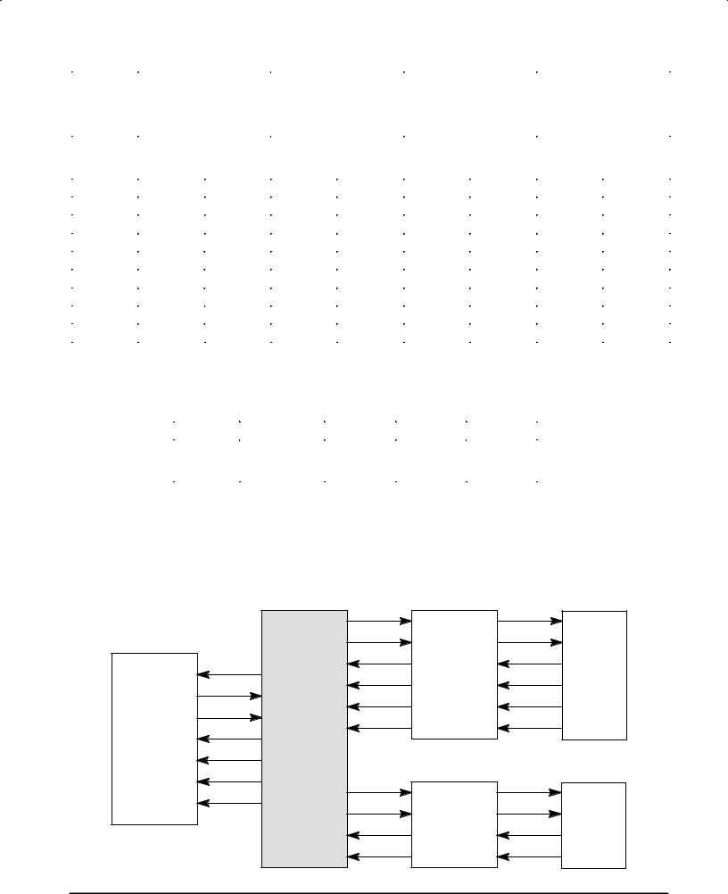
MC68160 MC68160B MC68160C
Figure 1. 10Base±T Interface Block Diagram
|
RX |
Manchester |
|
|
Mux |
Data |
ARX+ |
|
|
RCLK |
|
Decoder |
|
|
Receiver |
||
|
|
|
|
|
||||
|
MFILT |
|
|
|
|
|
|
|
|
RXLED |
Pulse Conditioner |
Carrier |
|
|
|
Noise |
ARX± |
|
|
Mux |
|
Reject |
||||
|
RENA |
|
Detect |
|
|
|
||
|
|
|
|
|
Filter |
|
||
|
CLLED |
Pulse Conditioner |
|
|
|
|
|
|
|
|
|
|
|
|
|
||
|
CLSN |
|
|
|
Collision |
|
Noise |
ACX+ |
INTERFACE |
Encoder |
Mux |
|
Detect |
|
Reject |
ACX± |
|
TX |
Mux |
|
|
|
Filter |
ATX+ |
||
|
TXLED |
Pulse |
|
|
|
|
ATX± |
|
|
TENA |
Conditioner |
|
|
|
|
|
|
|
Manchester |
|
|
|
|
|
|
|
SIA |
X1 |
20 MHz |
|
|
|
|
Receiver |
Twisted |
|
X2 |
Osc |
|
|
|
|
||
|
|
|
|
|
Mux |
Pair |
||
|
TCLK |
|
|
|
|
|
||
|
|
|
|
Collision |
|
|
Polarity |
|
|
|
2 |
|
|
|
|
Error |
|
|
|
|
|
|
Detector |
|
|
|
|
CS0 |
Jabber |
Driver |
Link |
Control |
|
|
Control |
|
|
|
Receiver |
|
||||
|
CS1 |
Pre±emphasis |
Pulse |
|
|
|
||
|
Control |
|
|
|
||||
|
CS2 |
Control |
Control |
|
|
Squelch |
|
|
|
TPEN |
Mode |
Squelch |
|
|
|
||
|
|
|
|
|
|
|||
|
APORT |
Select |
|
|
Test |
|
|
|
TPAPCE |
|
|
|
|
|
|||
|
|
|
Circuit |
|
|
|
||
TPSQEL |
|
|
|
|
|
|
||
TPFULDL |
|
|
|
|
|
|
|
|
|
LOOP |
|
|
|
|
|
|
|
|
|
TPJABB |
TPTX+ TPTX± |
TPLIL |
TPSQEL |
|
TPRX± |
TPRX+ TPPLR |
AUI INTERFACE
This device contains 20,000 active transistors.
2 |
MOTOROLA ANALOG IC DEVICE DATA |

MC68160 MC68160B MC68160C
Enhanced Ethernet Serial Transceiver
Table 1. Pin Descriptions . . . . . . . . . . . . . . . . . . . . . . . . . . . . . . . . . . . . . . . . . . . . . . . . . . . . . . . . . . . . . . . . . . . . . . . . . . . . . . . . . . 4 Controller Interface Pins . . . . . . . . . . . . . . . . . . . . . . . . . . . . . . . . . . . . . . . . . . . . . . . . . . . . . . . . . . . . . . . . . . . . . . . . . . . . . . . . . . . . . 4 AUI Interface Pins . . . . . . . . . . . . . . . . . . . . . . . . . . . . . . . . . . . . . . . . . . . . . . . . . . . . . . . . . . . . . . . . . . . . . . . . . . . . . . . . . . . . . . . . . . . 4 Twisted Pair Interface Pins . . . . . . . . . . . . . . . . . . . . . . . . . . . . . . . . . . . . . . . . . . . . . . . . . . . . . . . . . . . . . . . . . . . . . . . . . . . . . . . . . . . 4 Oscillator and Frequency Multiplier Pins . . . . . . . . . . . . . . . . . . . . . . . . . . . . . . . . . . . . . . . . . . . . . . . . . . . . . . . . . . . . . . . . . . . . . . . . 5 Mode Select Pins . . . . . . . . . . . . . . . . . . . . . . . . . . . . . . . . . . . . . . . . . . . . . . . . . . . . . . . . . . . . . . . . . . . . . . . . . . . . . . . . . . . . . . . . . . . 5 Status Indicator Pins . . . . . . . . . . . . . . . . . . . . . . . . . . . . . . . . . . . . . . . . . . . . . . . . . . . . . . . . . . . . . . . . . . . . . . . . . . . . . . . . . . . . . . . . 6 Power Supply and Ground Pins . . . . . . . . . . . . . . . . . . . . . . . . . . . . . . . . . . . . . . . . . . . . . . . . . . . . . . . . . . . . . . . . . . . . . . . . . . . . . . . 6
Table 2. Controller Interface Selection . . . . . . . . . . . . . . . . . . . . . . . . . . . . . . . . . . . . . . . . . . . . . . . . . . . . . . . . . . . . . . . . . . . . . 7
Table 3. Controller Independent Mode Selection . . . . . . . . . . . . . . . . . . . . . . . . . . . . . . . . . . . . . . . . . . . . . . . . . . . . . . . . . . |
7 |
Electrical Characteristics . . . . . . . . . . . . . . . . . . . . . . . . . . . . . . . . . . . . . . . . . . . . . . . . . . . . . . . . . . . . . . . . . . . . . . . . . . . . . . . . . . 8
Maximum Ratings . . . . . . . . . . . . . . . . . . . . . . . . . . . . . . . . . . . . . . . . . . . . . . . . . . . . . . . . . . . . . . . . . . . . . . . . . . . . . . . . . . . . . . . . . . . 8
Recommended Operating Conditions . . . . . . . . . . . . . . . . . . . . . . . . . . . . . . . . . . . . . . . . . . . . . . . . . . . . . . . . . . . . . . . . . . . . . . . . . . 8
ESD . . . . . . . . . . . . . . . . . . . . . . . . . . . . . . . . . . . . . . . . . . . . . . . . . . . . . . . . . . . . . . . . . . . . . . . . . . . . . . . . . . . . . . . . . . . . . . . . . . . . . . . 8
DC Characteristics . . . . . . . . . . . . . . . . . . . . . . . . . . . . . . . . . . . . . . . . . . . . . . . . . . . . . . . . . . . . . . . . . . . . . . . . . . . . . . . . . . . . . . . . 8 Power Supply DC Characteristics . . . . . . . . . . . . . . . . . . . . . . . . . . . . . . . . . . . . . . . . . . . . . . . . . . . . . . . . . . . . . . . . . . . . . . . . . . . . . 8 TTL/CMOS Input and Output DC Characteristics . . . . . . . . . . . . . . . . . . . . . . . . . . . . . . . . . . . . . . . . . . . . . . . . . . . . . . . . . . . . . . . . 9 Twisted Pair Input and Output DC Characteristics . . . . . . . . . . . . . . . . . . . . . . . . . . . . . . . . . . . . . . . . . . . . . . . . . . . . . . . . . . . . . . . 9 AUI Input and Output DC Characteristics . . . . . . . . . . . . . . . . . . . . . . . . . . . . . . . . . . . . . . . . . . . . . . . . . . . . . . . . . . . . . . . . . . . . . . 10
AC Characteristics . . . . . . . . . . . . . . . . . . . . . . . . . . . . . . . . . . . . . . . . . . . . . . . . . . . . . . . . . . . . . . . . . . . . . . . . . . . . . . . . . . . . . . . 12 External Clock Input (X1) Switching Characteristics . . . . . . . . . . . . . . . . . . . . . . . . . . . . . . . . . . . . . . . . . . . . . . . . . . . . . . . . . . . . . 12 Receive Phase Locked Loop Switching Characteristics . . . . . . . . . . . . . . . . . . . . . . . . . . . . . . . . . . . . . . . . . . . . . . . . . . . . . . . . . . 12 Controller Transmit Switching Characteristics (Motorola Mode) . . . . . . . . . . . . . . . . . . . . . . . . . . . . . . . . . . . . . . . . . . . . . . . . . . . 12 Controller Receive Switching Characteristics (Motorola Mode) . . . . . . . . . . . . . . . . . . . . . . . . . . . . . . . . . . . . . . . . . . . . . . . . . . . . 12 Controller Transmit Switching Characteristics (Intel Mode) . . . . . . . . . . . . . . . . . . . . . . . . . . . . . . . . . . . . . . . . . . . . . . . . . . . . . . . 14 Controller Receive Switching Characteristics (Intel Mode) . . . . . . . . . . . . . . . . . . . . . . . . . . . . . . . . . . . . . . . . . . . . . . . . . . . . . . . . 14 Controller Transmit Switching Characteristics (Fujitsu Mode) . . . . . . . . . . . . . . . . . . . . . . . . . . . . . . . . . . . . . . . . . . . . . . . . . . . . . 15 Controller Receive Switching Characteristics (Fujitsu Mode) . . . . . . . . . . . . . . . . . . . . . . . . . . . . . . . . . . . . . . . . . . . . . . . . . . . . . 15 Controller Transmit Switching Characteristics (National Mode) . . . . . . . . . . . . . . . . . . . . . . . . . . . . . . . . . . . . . . . . . . . . . . . . . . . . 16 Controller Receive Switching Characteristics (National Mode) . . . . . . . . . . . . . . . . . . . . . . . . . . . . . . . . . . . . . . . . . . . . . . . . . . . . 16 TP Transmit Switching Characteristics . . . . . . . . . . . . . . . . . . . . . . . . . . . . . . . . . . . . . . . . . . . . . . . . . . . . . . . . . . . . . . . . . . . . . . . . 18 TP Transmit Jabber Switching Characteristics . . . . . . . . . . . . . . . . . . . . . . . . . . . . . . . . . . . . . . . . . . . . . . . . . . . . . . . . . . . . . . . . . . 20 TP Transmit Signal Quality Error Test Switching Characteristics . . . . . . . . . . . . . . . . . . . . . . . . . . . . . . . . . . . . . . . . . . . . . . . . . . 20 TP Receive Switching Characteristics . . . . . . . . . . . . . . . . . . . . . . . . . . . . . . . . . . . . . . . . . . . . . . . . . . . . . . . . . . . . . . . . . . . . . . . . . 21 TP Receive Link Integrity Switching Characteristics . . . . . . . . . . . . . . . . . . . . . . . . . . . . . . . . . . . . . . . . . . . . . . . . . . . . . . . . . . . . . 21 TP Collision Switching Characteristics . . . . . . . . . . . . . . . . . . . . . . . . . . . . . . . . . . . . . . . . . . . . . . . . . . . . . . . . . . . . . . . . . . . . . . . . 23 TP Full Duplex Switching Characteristics . . . . . . . . . . . . . . . . . . . . . . . . . . . . . . . . . . . . . . . . . . . . . . . . . . . . . . . . . . . . . . . . . . . . . . 23 AUI Transmit Switching Characteristics . . . . . . . . . . . . . . . . . . . . . . . . . . . . . . . . . . . . . . . . . . . . . . . . . . . . . . . . . . . . . . . . . . . . . . . 24 AUI Receive Switching Characteristics . . . . . . . . . . . . . . . . . . . . . . . . . . . . . . . . . . . . . . . . . . . . . . . . . . . . . . . . . . . . . . . . . . . . . . . . 24
Functional Description . . . . . . . . . . . . . . . . . . . . . . . . . . . . . . . . . . . . . . . . . . . . . . . . . . . . . . . . . . . . . . . . . . . . . . . . . . . . . . . . . . . 25
Data Transmission . . . . . . . . . . . . . . . . . . . . . . . . . . . . . . . . . . . . . . . . . . . . . . . . . . . . . . . . . . . . . . . . . . . . . . . . . . . . . . . . . . . . . . . . . 25
Data Reception . . . . . . . . . . . . . . . . . . . . . . . . . . . . . . . . . . . . . . . . . . . . . . . . . . . . . . . . . . . . . . . . . . . . . . . . . . . . . . . . . . . . . . . . . . . . 26
Collision . . . . . . . . . . . . . . . . . . . . . . . . . . . . . . . . . . . . . . . . . . . . . . . . . . . . . . . . . . . . . . . . . . . . . . . . . . . . . . . . . . . . . . . . . . . . . . . . . . 26
Jabber . . . . . . . . . . . . . . . . . . . . . . . . . . . . . . . . . . . . . . . . . . . . . . . . . . . . . . . . . . . . . . . . . . . . . . . . . . . . . . . . . . . . . . . . . . . . . . . . . . . . 26
Full Duplex . . . . . . . . . . . . . . . . . . . . . . . . . . . . . . . . . . . . . . . . . . . . . . . . . . . . . . . . . . . . . . . . . . . . . . . . . . . . . . . . . . . . . . . . . . . . . . . . 26
Auto Port Selection . . . . . . . . . . . . . . . . . . . . . . . . . . . . . . . . . . . . . . . . . . . . . . . . . . . . . . . . . . . . . . . . . . . . . . . . . . . . . . . . . . . . . . . . . 26
Auto Polarity Selection . . . . . . . . . . . . . . . . . . . . . . . . . . . . . . . . . . . . . . . . . . . . . . . . . . . . . . . . . . . . . . . . . . . . . . . . . . . . . . . . . . . . . . 26
Loop Back Mode . . . . . . . . . . . . . . . . . . . . . . . . . . . . . . . . . . . . . . . . . . . . . . . . . . . . . . . . . . . . . . . . . . . . . . . . . . . . . . . . . . . . . . . . . . . 26
Applications . . . . . . . . . . . . . . . . . . . . . . . . . . . . . . . . . . . . . . . . . . . . . . . . . . . . . . . . . . . . . . . . . . . . . . . . . . . . . . . . . . . . . . . . . . . . . . 27 Selection of Crystal and External Components . . . . . . . . . . . . . . . . . . . . . . . . . . . . . . . . . . . . . . . . . . . . . . . . . . . . . . . . . . . . . . . . . 27 PLL Filter Components . . . . . . . . . . . . . . . . . . . . . . . . . . . . . . . . . . . . . . . . . . . . . . . . . . . . . . . . . . . . . . . . . . . . . . . . . . . . . . . . . . . . . 27 10BASE±T Filter and Transformer Choice . . . . . . . . . . . . . . . . . . . . . . . . . . . . . . . . . . . . . . . . . . . . . . . . . . . . . . . . . . . . . . . . . . . . . 27 AUI Transformer Choice . . . . . . . . . . . . . . . . . . . . . . . . . . . . . . . . . . . . . . . . . . . . . . . . . . . . . . . . . . . . . . . . . . . . . . . . . . . . . . . . . . . . 27
MOTOROLA ANALOG IC DEVICE DATA |
3 |
|

|
|
|
MC68160 MC68160B MC68160C |
|
|
|
|
|
Table 1. Pin Function Descriptiont |
|
|
|
|
|
Pin(s) |
Symbol |
Type |
|
Name/Function |
|
|
|
|
|
CONTROLLER INTERFACE |
|
|
||
|
|
|
|
|
1 |
RENA |
O |
|
Receive Enable Output: Indication of the presence of network activity, synchronous to |
|
|
TTL/CMO |
|
RCLK. In the standby mode, RENA is driven to the high impedance state. |
|
|
|
|
|
2 |
RX |
O |
|
Receive Data Output: Recovered data, synchronous to RCLK. Following a reset operation, |
|
|
TTL/CMOS |
|
100 ms should be allowed before attempting to read data processed by the MC68160, B and |
|
|
|
|
C. This delay is needed to insure that the receive phase locked loop is properly synchronized |
|
|
|
|
with incoming data. In the standby mode, RX is driven to the high impedance state. |
|
|
|
|
|
48 |
TCLK |
O |
|
Transmit Clock Output CMOS/TTL Output: TCLK provides a symmetrical clock signal at |
|
|
TTL/CMOS |
|
10 MHz for reference timing of data to be encoded. In the standby mode, TCLK is driven to |
|
|
|
|
the high impedance state. |
|
|
|
|
|
49 |
TENA |
I |
|
Transmit Enable Input: Input signal synchronous to TCLK which enables data transmission |
|
|
TTL |
|
on the active port. An internal pull±down resistor is provided so that the input is low under no |
|
|
|
|
connect conditions. (This resistor is removed in the standby mode). If TENA is asserted at |
|
|
|
|
the conclusion of a reset operation, it must first be deasserted and then reasserted before |
|
|
|
|
data transmission can occur. In the standby mode, TENA is driven to the high impedance |
|
|
|
|
state. |
|
|
|
|
|
50 |
RCLK |
O |
|
Receive Clock Output: Recovered clock. In the standby mode, RCLK is driven to the high |
|
|
TTL/CMOS |
|
impedance state. |
|
|
|
|
|
51 |
CLSN |
O |
|
Collision Output: In the AUI mode, indicates the presence of signals at the ACX+ and |
|
|
TTL/CMOS |
|
ACX± terminals which meet threshold and pulse width requirements. In the TP mode, |
|
|
|
|
indicates simultaneous transmit and receive activity, a heartbeat (SQE Test) signal was |
|
|
|
|
generated, or the jabber timer has expired. In the standby mode, CLSN is driven to the high |
|
|
|
|
impedance state. |
|
|
|
|
|
52 |
TX |
I |
|
Transmit Data Input: Input signal synchronous to TCLK which provides NRZ serial data to |
|
|
TTL |
|
be Manchester encoded. In the standby mode, TX is driven to the high impedance state. |
|
|
|
|
|
AUI INTERFACE |
|
|
|
|
|
|
|
|
|
21 |
ACX± |
I |
|
AUI Differential Collision Inputs: These inputs are connected to a pair of internally biased |
22 |
ACX+ |
|
|
line receivers consisting of a carrier detect receiver with offset threshold and noise filtering to |
|
|
|
|
detect the line activity. Signals at ACX+/± have no effect on data path functions. |
|
|
|
|
|
23 |
ARX± |
I |
|
AUI Differential Receiver Inputs: These inputs are connected to a pair of internally biased |
24 |
ARX+ |
|
|
line receivers consisting of a carrier detect receiver with offset threshold and noise filtering to |
|
|
|
|
detect the line activity, and a data receiver with no offset for Manchester Data reception. |
|
|
|
|
|
25 |
ATX± |
O |
|
AUI Differential Transmit Outputs : This line pair is intended to operate into terminated |
26 |
ATX+ |
|
|
transmission lines. For TX signals meeting setup and hold time to TCLK when TENA is |
|
|
|
|
previously asserted, Manchester encoded data is outputted at ATX+/±. When operating into a |
|
|
|
|
78 Ω terminated transmission line, signaling meets the required output levels and skew for |
|
|
|
|
IEEE±802.3 drop cables. When the 10BASE±T port is automatically or manually selected, |
|
|
|
|
the AUI outputs are driven to a low power standby state in which the outputs deliver a |
|
|
|
|
balanced high state voltage. |
|
|
|
|
|
TWISTED PAIR INTERFACE |
|
|
||
|
|
|
|
|
31 |
TPRX± |
I |
|
Twisted Pair Differential Receiver Inputs: These inputs are connected to a receiver with |
32 |
TPRX+ |
|
|
Smart Squelch capability which only allows differential receive data to pass as long as the |
|
|
|
|
input amplitude is greater than a minimum signal threshold level and a specific pulse |
|
|
|
|
sequence is received. This assures a good signal to noise ratio while the signal pair is active |
|
|
|
|
by preventing crosstalk and impulse noise conditions from activating the receive function. |
|
|
|
|
|
36 |
TPTX± |
O |
|
Twisted Pair Differential Transmitter Outputs: These lines have pre±distortion drive |
37 |
TPTX+ |
|
|
capability and are intended to drive terminated twisted pair transmission lines. When the AUI |
|
|
|
|
port is manually selected, the 10BASE±T outputs are driven to a low power standby state in |
|
|
|
|
which the outputs deliver a balanced high state voltage. However, when the AUI port is |
|
|
|
|
automatically selected, the 10BASE±T outputs remain active. |
|
|
|
|
|
NOTE: The sense of the controller interface pins will change, depending on the controller selected.
4 |
MOTOROLA ANALOG IC DEVICE DATA |

|
|
MC68160 MC68160B MC68160C |
|
|
|
Table 1. Pin Function Description (continued) |
|
|
|
|
|
Pin(s) |
Symbol |
Type |
Name/Function |
|
|
|
|
OSCILLATOR AND FREQUENCY MULTIPLIER |
|||
|
|
|
|
12 |
MFILT |
C |
Frequency Multiplier Filter Connection Point: An external resistor capacitor filter must be |
|
|
|
attached to this pin. |
|
|
|
|
16 |
X1 |
I/C |
Oscillator Inverter Input and Crystal Connection Point: When connected for crystal |
|
|
CMOS |
oscillator operation, the frequency of the clock which appears at TCLK is half that of the |
|
|
|
crystal oscillator. As an option, instead of connecting to a crystal, X1 may be driven from an |
|
|
|
external 20 MHz CMOS compatible clock generator. |
|
|
|
|
17 |
X2 |
O/C |
Oscillator Inverter Output and Crystal Connection Point: This pin is used only for the |
|
|
CMOS |
connection of an external crystal and capacitor. It must be left unconnected if X1 is driven by |
|
|
|
an external CMOS Clock generator. |
|
|
|
|
MODE SELECT |
|
|
|
|
|
|
|
3 |
CS0 |
I |
Mode Select: The logic states applied to these pins select the appropriate interface for the |
4 |
CS1 |
TTL |
desired IEEE±802.3 controller or enable the standby mode. When the standby mode is |
5 |
CS2 |
|
selected, the MC68160, B and C power supply current is greatly reduced. Additionally, in the |
|
|
|
standby mode, all of the controller inputs and outputs are driven to the high impedance state. |
|
|
|
|
6 |
LOOP |
I |
Diagnostic Loopback: Asserting this function causes serial NRZ data at the TX input to be |
|
|
TTL |
Manchester encoded and then looped back through the Manchester decoder, appearing at |
|
|
|
the RX output. This diagnostic loopback function operates independent of Twisted Pair (TP) |
|
|
|
or Access Unit Interface (AUI) port connectivity or activity. Neither the TP port nor the AUI |
|
|
|
port transmits data from the controller while diagnostic loopback is selected. Likewise, the |
|
|
|
controller interface receives data neither from the TP nor the AUI receivers while in this |
|
|
|
mode. The polarity fault detection and link integrity functions are not inhibited by the |
|
|
|
diagnostic loopback mode. If otherwise enabled, they continue to function. If the twisted pair |
|
|
|
port is selected, and TPSQEL is driven to the low logic state, a collision detect pulse is |
|
|
|
delivered following each transmission to simulate the twisted pair SQE test. |
|
|
|
|
9 |
APORT |
I |
Automatic Port Selection Enable: When high, MC68160, B and C will automatically select |
|
|
TTL |
the TP or AUI port based on the presence or absence of valid link beats or frames at the TP |
|
|
|
receive input. If the AUI port is automatically selected, the MC68160, B and C will continue to |
|
|
|
produce link pulses for the TP port. Changing ports requires approximately 1.0 ms to allow |
|
|
|
the circuitry |
|
|
|
for the new port to resume normal operation. The power consumption is minimized in the |
|
|
|
circuitry associated with the unselected port. |
|
|
|
|
27 |
TPSQEL |
I |
Twisted Pair Signal Quality Error Test Enable: Forcing this pin low enables testing of the |
|
|
TTL |
internal TP collision detect circuitry after each transmit operation to the TP media. This |
|
|
|
function provides a simulated collision to as much of the MC68160, B and C collision detect |
|
|
|
circuitry as possible without affecting the attached twisted pair channel. A normal SQE test |
|
|
|
results in a high logic state at the CLSN controller interface pin which begins 6 to 16±bit |
|
|
|
times after the last transition of a transmitted signal and continues for 5 to 15±bit times. |
|
|
|
(When the AUI port is selected, SQE test signals are generated by the coaxial cable |
|
|
|
transceiver and delivered to the controller via the MC68160, B and C ACX+/± receive inputs) |
|
|
|
|
28 |
TPFULDL |
I |
Twisted Pair Full Duplex Mode Select: Forcing this pin low allows simultaneous transmit |
|
|
TTL |
and receive operation on the twisted pair port without an indicated collision. This pin is not to |
|
|
|
be asserted with LOOP as a test mode is enabled that disrupts normal operation. |
|
|
|
|
29 |
TPAPCE |
I |
Twisted Pair Automatic Polarity Correction Enable: When TPAPCE is high, automatic |
|
|
TTL |
polarity correction is enabled, and MC68160, B and C will internally correct for a polarity fault |
|
|
|
on the receive circuit. Additionally, when TPAPCE is high, the presence of a polarity fault is |
|
|
|
indicated on TPPLR. |
|
|
|
|
46 |
TPEN |
I/O |
Twisted Pair Port Enable: If APORT is low, TPEN is an input which determines whether the |
|
|
TTL |
AUI port (TPEN low) or TP port (TPEN high) will be manually selected. If the AUI port is |
|
|
(TTL/CMOS) |
manually selected, the MC68160, B and C will not produce link pulses for the TP port. |
|
|
|
If APORT is high, TPEN is an output which will indicate which port has been automatically |
|
|
|
selected by driving TPEN low (for AUI) or high (for TP). In its output mode TPEN can sink |
|
|
|
10 mA in the low output state and source 10 mA in the high output state. (See Pin 9 |
|
|
|
Description.) |
|
|
|
Changing ports requires approximately 1.0 ms to allow the circuitry for the new port to |
|
|
|
resume normal operation. The power consumption is minimized in the circuitry associated |
|
|
|
with the unselected port. In the standby mode, this pin is driven to the high impedance state. |
|
|
|
|
MOTOROLA ANALOG IC DEVICE DATA |
5 |
|

MC68160 MC68160B MC68160C
Table 1. Pin Function Description (continued)
Pin(s) |
Symbol |
Type |
Name/Function |
|
|
|
|
STATUS INDICATOR
40 |
TXLED |
O |
Transmit Status LED Driver Output: This pin indicates the transmit status of the currently |
|
|
TTL/CMOS |
selected TP or AUI port. When there is no transmit activity detected, an internal pull±up takes |
|
|
|
this pin to its normal off (high) state. When transmit activity is detected, the LED driver turns |
|
|
|
on. In its on state, TXLED flashes the LED by driving low at approximately 10 Hz at a 50% |
|
|
|
duty cycle. In the standby mode, this output is driven to the high impedance state. |
|
|
|
|
41 |
RXLED |
O |
Receive Status LED Driver Output: This pin indicates the receive status of the currently |
|
|
TTL/CMOS |
selected TP or AUI port. When there is no receive activity detected, an internal pull±up takes |
|
|
|
this pin to its normal off (high) state. When receive activity is detected, the LED driver turns |
|
|
|
on. In its on state, RXLED flashes the LED by driving low at approximately 10 Hz at a 50% |
|
|
|
duty cycle. In the standby mode, this output is driven to the high impedance state. |
|
|
|
|
42 |
CLLED |
O |
Collision Status LED Driver Output: This pin indicates the collision status of the currently |
|
|
TTL/CMOS |
selected TP or AUI port. When there is no collision activity detected, an internal pull±up takes |
|
|
|
this pin to its normal off (high) state. When collision activity is detected, the LED driver turns |
|
|
|
on. In its on state, CLLED flashes the LED by driving low at approximately 10 Hz at a 50% |
|
|
|
duty cycle. In the standby mode, this output is driven to the high impedance state. |
|
|
|
|
43 |
TPLIL |
O |
Twisted Pair Link Integrity Output: This output is driven to the low output state to indicate |
|
|
TTL/CMOS |
good link integrity on the TP port during TP mode. It is deasserted (high) when link integrity |
|
|
|
fails in TP mode. The TPLIL output is driven to the high impedance state when the AUI port |
|
|
|
is selected. In the standby mode, this output is also driven to the high impedance state. |
|
|
|
|
44 |
TPPLR |
O |
Twisted Pair Polarity Error Output: If TPAPCE is high and the wires connected to the |
|
|
TTL/CMOS |
Twisted Pair Receiver Inputs (TPRX+, TPRX±) are reversed, TPPLR will be driven to the low |
|
|
|
logic state to indicate the fault. TPPLR remains low when the MC68160, B and C has |
|
|
|
automatically corrected for the reversed wires. If the twisted pair link integrity tests fail, this |
|
|
|
output will be driven to the high logic state. When the AUI mode is selected this output is |
|
|
|
driven to the high impedance state. In the standby mode, this output is also driven to the high |
|
|
|
impedance state. |
|
|
|
|
45 |
TPJABB |
O |
Twisted Pair Jabber Output: This pin is driven high to indicate a jabber condition at the |
|
|
TTL/CMOS |
TPTX+/± outputs. (Jabber condition also causes CLLED to be driven alternately to the high |
|
|
|
and low output levels). TPJABB is driven to the low output state when no jabber condition is |
|
|
|
present. When the AUI mode is selected this output is driven to the high impedance state. In |
|
|
|
the standby mode, this output is also driven to the high impedance state. |
|
|
|
|
POWER SUPPLY AND GROUND
10 |
|
VDDDIV |
|
Frequency Divider Supply Pin |
|
|
|
|
|
11 |
|
VDDFM |
|
Frequency Multiplier Supply and Ground Pins |
13 |
|
GNDFM |
|
|
|
|
|
|
|
14 |
|
GNDVCO |
|
Voltage Controlled Oscillator Ground and Supply Pins |
15 |
|
VDDVCO |
|
|
|
|
|
|
|
20 |
|
GNDSUB |
|
Substrate Ground Pin |
|
|
|
|
|
7 |
|
VDDDIG |
|
Digital Supply and Ground Pins |
8 |
|
GNDDIG |
|
|
18 |
|
VDDDIG |
|
|
19 |
|
GNDDIG |
|
|
|
|
|
|
|
30 |
|
VDDANA |
|
Analog Supply and Ground Pins |
33 |
|
GNDANA |
|
|
|
|
|
|
|
34 |
|
GNDPWR |
|
Power Supply and Ground Pins |
35 |
|
VDDPWR |
|
|
38 |
|
VDDPWR |
|
|
39 |
|
GNDPWR |
|
|
|
|
|
|
|
47 |
|
GNDCTL |
|
Controller Interface Ground Pin |
|
|
|
|
|
NOTE: |
Power and ground pins are not connected internally. Failure to connect externally may cause malfunction or damage to the IC. |
|||
6 |
MOTOROLA ANALOG IC DEVICE DATA |
MC68160 MC68160B MC68160C
Table 2. Controller Interface Selection
Motorola |
|
Motorola |
|
|
|
|
|
|
Intel4 |
|
Fujitsu4 |
National4 |
|||||
Transceiver |
Controller2 |
|
|
Controllers |
Controllers |
Controllers |
|||||||||||
MC68160, |
MC68360 |
82586, 82590, |
86950 (Etherstar ) |
8390, 83C690, |
|||||||||||||
B and C |
(QUICC ) |
82593, 82596 |
86960 (NICE ) |
83932B (SONIC ) |
|||||||||||||
(EEST ) |
|
|
|
|
|
|
|
|
|
|
|
|
|
|
|
|
|
|
|
|
|
|
|
|
|
|
|
|
|
|
|
|
|
|
|
CS0 |
|
1 |
|
|
|
|
|
|
0 |
|
1 |
|
0 |
||||
CS1 |
|
1 |
|
|
|
|
|
|
1 |
|
0 |
|
0 |
||||
CS2 |
|
0 |
|
|
|
|
|
|
0 |
|
0 |
|
0 |
||||
|
|
|
|
|
|
|
|
|
|
|
|
|
|
|
|
|
|
Pin |
Pin |
|
Sense |
|
|
Pin |
|
Sense |
Pin |
|
Sense |
Pin |
|
Sense |
|||
|
|
|
|
|
|
|
|
|
|
|
|
|
|
|
|
|
|
|
|
|
|
|
|
|
|
|
|
|
|
|
|
|
|
|
|
TCLK |
TCLK |
|
High |
|
|
TXC |
|
Low |
TCKN |
|
Low |
TXC |
|
High |
|||
|
|
|
|
|
|
|
|
|
|
|
|
|
|
|
|
|
|
TX |
TX |
|
High |
|
|
TXD |
|
High |
TXD |
|
High |
TXD |
|
High |
|||
|
|
|
|
|
|
|
|
|
|
|
|
|
|
|
|
|
|
|
|
|
|
|
|
|
|
|
|
|
|
|
|
|
|
|
|
TENA |
TENA |
|
High |
|
|
RTS |
|
Low |
TEN |
|
High |
TXE |
|
High |
|||
|
|
|
|
|
|
|
|
|
|
|
|
|
|
|
|
|
|
|
|
|
|
|
|
|
|
|
|
|
|
|
|
|
|
|
|
RCLK |
RCLK |
|
High |
|
RXC |
|
Low |
RCN |
|
Low |
RXC |
|
High |
||||
|
|
|
|
|
|
|
|
|
|
|
|
|
|
|
|
|
|
RX |
RX |
|
High |
|
RXD |
|
High |
RXD |
|
High |
RXD |
|
High |
||||
|
|
|
|
|
|
|
|
|
|
|
|
|
|
|
|
|
|
|
|
|
|
|
|
|
|
|
|
|
|
|
|
|
|
|
|
RENA |
RENA |
|
High |
|
CRS |
|
Low |
XCD |
|
High |
CRS |
|
High |
||||
|
|
|
|
|
|
|
|
|
|
|
|
|
|
|
|
|
|
|
|
|
|
|
|
|
|
|
|
|
|
|
|
|
|
|
|
CLSN |
CLSN |
|
High |
|
|
CDT |
|
Low |
XCOL |
|
Low |
COL |
|
High |
|||
|
|
|
|
|
|
|
|
|
|
|
|
|
|||||
LOOP1 |
|
|
|
|
|
|
|
|
|
|
|
|
|
|
|
|
|
N.A. |
|
High |
LPBK |
|
Low |
LBC |
|
High |
LPBK |
|
High |
||||||
NOTES: 1. Although LOOP input is not ordinarily classifed as a controller pin, it is included in this table because its sense varies according to the controller used.
2.The Motorola controller interface contained in the MC68360 (QUICC ) is compatible with the AMD 7990 (LANCE ) and 79C900 (ILACC ) controllers.
3.The pin sense is shown from the perspective of the identified controller pin.
4.Supported only by MC68160.
Table 3. Controller Independent Mode Selection
Pin |
Standby Mode |
Reserved |
Reserved |
Reserved |
|
|
|
|
|
CS0 |
1 |
0 |
1 |
0 |
CS1 |
1 |
1 |
0 |
0 |
CS2 |
1 |
1 |
1 |
1 |
|
|
|
|
|
NOTE: In standby mode, the MC68160, B, C consumes less power supply current than in any other mode. Additionally, in the standby mode, all of the controller inputs and outputs are driven to the high impedance state. When the standby mode is deasserted, an internal reset pulse of approximately 6.0 μs duration is generated.
Following a period of operation in the standby mode, the time required to insure stable data reception is approximately 100 ms.
Figure 2. Applications Block Diagram
|
|
ATX+ |
|
ATX+ |
|
|
|
ATX± |
|
ATX± |
|
|
TCLK |
ARX+ |
Pulse |
ARX+ |
DB±15 |
|
ARX± |
ARX± |
|||
|
TX |
Transformers |
Connector |
||
|
ACX+ |
|
ACX+ |
|
|
|
|
|
|
||
|
TENA |
ACX± |
|
ACX± |
|
LAN |
RCLK |
|
|
||
MC68160, B, C |
|
|
|
||
Controller |
|
|
|
||
|
|
|
|
||
|
|
|
|
|
|
|
RX |
|
|
|
|
|
RENA |
TPTX+ |
|
TPTX+ |
|
|
CLSN |
|
|
||
|
TPTX± |
Filters |
TPTX± |
|
|
|
|
RJ±45 |
|||
|
|
TPRX+ |
and |
TPRX+ |
|
|
|
Pulse |
Connector |
||
|
|
|
|
||
|
|
TPRX± |
Transformers |
TPRX± |
|
MOTOROLA ANALOG IC DEVICE DATA |
7 |
|

MC68160 MC68160B MC68160C
ELECTRICAL CHARACTERISTICS
MAXIMUM RATINGS
Characteristic |
Symbol |
Min |
Max |
|
Unit |
|
|
|
|
|
|
Storage Temperature Range |
Tstg |
± 65 |
150 |
|
°C |
Power Supply Voltage Range |
|
|
|
|
|
Analog |
VDDA |
± |
7.0 |
|
V |
Digital |
VDDD |
± |
7.0 |
|
|
Voltage on any TTL compatible input pin with |
V |
± 0.5 |
VDD + 0.5 |
|
V |
respect to Ground |
|
|
|
|
|
Voltage on TPRX, ARX, or ACX input pins with |
|
± 0.5 |
6.0 |
|
|
respect to Ground |
|
|
|
|
|
|
|
|
|
|
|
Differential Voltage on TPRX, ARX, or ACX Input |
VDIFF |
± 6.0 |
6.0 |
|
V |
Pins |
|
|
|
|
|
|
|
|
|
|
|
NOTE: Stresses in excess of the Absolute Maximum Ratings can cause permanent damage to the |
|
||||
device. Functional operation of the device is not implied at these or any other conditions in |
|
||||
excess of those indicated in the operation sections of this data sheet. Exposure to Absolute |
|
||||
Maximum Ratings conditions for extended periods can adversely affect device reliability. |
|
||||
RECOMMENDED OPERATING CONDITIONS
Characteristic |
Symbol |
Min |
Max |
Unit |
|
|
|
|
|
Power Supply Voltage Range |
VDD |
4.75 |
5.25 |
V |
Power Supply Ripple (20 kHz to 100 kHz) |
± |
± |
50 |
mV |
|
|
|
|
|
Power Supply Impulse Noise (Either Polarity) |
± |
± |
100 |
mV |
|
|
|
|
|
Ambient Operating Temperature Range (MC68160, MC68160C) |
TA |
0 |
70 |
°C |
Ambient Operating Temperature Range (MC68160B) |
TA |
±40 |
85 |
°C |
ARX/ACX Input Differential Rise and Fall Time (see Figure 39) |
t260 |
2.0 |
10 |
ns |
ARX Pair Idle Time after Transmission (see Figure 39) |
t265 |
8.0 |
± |
μs |
ESD
Although protection circuitry has been designed into this device, proper precautions should be taken to avoid exposure to electrostatic discharge
(ESD) during handling and mounting. Motorola employs a Human Body Model (HBM) and a Charged Device Model (CDM) for ESD±susceptibility testing and protection design evaluation. ESD has been adopted for the CDM, however, a standard HBM (resistance = 1500 Ω capacitance ±
100 pF) is widely used and, therefore, can be used for comparison purposes. The HBM ESD threshold presented here was obtained by using the circuit parameters contained in this specification. ESD threshold voltage is designed to 700 kV Human Body Model.
DC ELECTRICAL CHARACTERISTICS (Unless otherwise noted, minimum and maximum limits apply over the recommended ambient operating temperature and power supply voltage ranges.)
Characteristic |
Symbol |
Test Conditions |
Min |
Typ |
Max |
Unit |
|
|
|
|
|
|
|
POWER SUPPLY |
|
|
|
|
|
|
|
|
|
|
|
|
|
Undervoltage Shutdown Threshold |
± |
± |
± |
± |
4.4 |
V |
|
|
|
|
|
|
|
Power Supply Current |
IDD |
± |
± |
145 |
200 |
mA |
|
|
Standby Mode |
± |
± |
5.0 |
|
|
|
|
|
|
|
|
8 |
MOTOROLA ANALOG IC DEVICE DATA |

MC68160 MC68160B MC68160C
DC ELECTRICAL CHARACTERISTICS (TA = 25°C, VCC = 5.0 V ± 5%. Unless otherwise noted, minimum and maximum
limits apply over the recommended ambient operating temperature and power supply voltage ranges for each MC68160, B, C except where noted.)
Characteristic |
Symbol |
Test Conditions |
Min |
Max |
Unit |
|
|
|
|
|
|
TTL COMPATIBLE INPUTS |
|
|
|
|
|
|
|
|
|
|
|
TTL Compatible Input Voltage |
|
± |
|
|
V |
Low State |
VIL(TTL) |
|
± |
0.8 |
|
High State |
VIH(TTL) |
|
2.0 |
± |
|
Input Current TTL Compatible Input Pins (Note 1) |
|
0 V < VI < VDD |
± |
±10 |
μA |
Input Current TENA TTL Compatible Input Pin: |
|
|
|
|
|
with Pull±Down Resistor |
|
|
|
|
|
IIH |
I |
|
± |
+200 |
|
IIL |
IH |
|
± |
± 20 |
|
I |
|
|
|||
with Pull±Down Resistor removed in Standby Mode |
IL |
|
± |
± |
|
IIH & IIL |
|
|
|||
|
|
10 |
|
||
CMOS COMPATIBLE INPUTS |
|
|
|
|
|
|
|
|
|
|
|
CMOS Compatible Input Voltage |
|
± |
|
|
V |
Low State |
VIL(CMOS) |
|
± |
1.0 |
|
High State |
VIH(CMOS) |
|
3.0 |
± |
|
Input Current (Pin X1) |
IIH & IIL |
0 V < VI < VDD |
± |
±100 |
μA |
TTL/CMOS COMPATIBLE OUTPUTS |
|
|
|
|
|
|
|
|
|
|
|
TTL/CMOS Compatible Output Voltage |
VOL |
|
|
|
V |
Low State (Note 2) |
|
IOL = 4.0 mA |
± |
0.45 |
|
Low State (Note 3) |
|
IOL = 10 mA |
± |
0.45 |
|
TTL/CMOS Compatible Output Voltage |
VOH |
|
|
|
V |
High State (Note 4) |
|
IOH = ± 500 μA |
3.9 |
± |
|
High State (Note 5) |
|
IOH = ± 10 mA |
3.9 |
± |
|
High State (Note 2) |
|
IOH = ± 4.0 mA |
2.4 |
± |
|
Three State Output Leakage Current |
IOZ |
0 V ≤ VOZ ≤ VDD |
± |
±10 |
μA |
Characteristic |
Symbol |
Test Conditions |
Min |
Max |
Unit |
|
|
|
|
|
|
TWISTED PAIR RECEIVER INPUTS |
|
|
|
|
|
|
|
|
|
|
|
Input Voltage Range (DC + AC) |
VITP |
± |
1.5 |
4.3 |
V |
Differential Input Squelch Threshold Voltage (MC68160, |
VITPSQ |
Note 10 |
270 |
390 |
mV |
MC68160C) |
|
|
|
|
|
|
|
|
|
|
|
Differential Input Squelch Threshold Voltage |
VITPSQ |
Note 10 |
260 |
400 |
mV |
(MC68160B) |
|
|
|
|
|
|
|
|
|
|
|
Common Mode Bias Generator Voltage |
VBCMTP |
Note 9 |
1.8 |
3.2 |
V |
Common Mode Input Resistance |
RCMTP |
± |
1000 |
± |
Ω |
Differential Input Resistance |
RDIFFTP |
± |
2.5 |
± |
kΩ |
TWISTED PAIR TRANSMITTER OUTPUTS |
|
|
|
|
|
|
|
|
|
|
|
Differential Output Voltage |
|
Note 7 |
|
|
V |
Pre±Emphasis Level |
VODFTPP |
|
± 2.2 |
±2.8 |
|
Signal Level (MC68160, MC68160C) |
VODFTPS |
|
±1.56 |
±1.98 |
|
Signal Level (MC68160B) |
VODFTPS |
|
±1.38 |
±1.98 |
|
Common Mode Output Voltage Range |
VOCMTP |
Note 6 |
0 |
4.0 |
V |
Common Mode Output Voltage in Standby Mode |
VOCMTPSB |
IOH = ±100 μA |
VDD ± 1.0 |
VDD |
V |
NOTES: 1. APORT, TPAPCE, CS0, CS1, CS2, TX, LOOP, TPFULDL, TPSQEL and TPEN (In Input Mode).
2.TCLK, RX, RCLK, RENA and CLSN.
3.TPPLR, TPLIL, TPJABB, TXLED, RXLED, CLLED and TPEN (In Output Mode).
4.TPPLR, TPLIL, CLLED, TXLED and RXLED.
5.TPJABB and TPEN (In Output Mode).
6.Measured with Test Load B1 (shown in Figure 3), applied directly to the TPTX+/± pins of the device.
7.Measured differentially with Test Load B2 (shown in Figure 4), applied directly to the TPTX+/± pins of the device.
8.Measured directly on the TPTX+/± pins of the device.
9.Measured with Test Load B3 (shown in Figure 5), applied directly to the TPRX+/± pins of the device.
10.The Common Mode Input Voltage is between 1.8 V and 3.2 V.
MOTOROLA ANALOG IC DEVICE DATA |
9 |
|
 Loading...