


Motorola MC68302CFC16, MC68302CFC20, MC68302RC25, MC68302PV16, MC68302PV16V Datasheet
...Microprocessors and Memory
Technologies Group
MC68302
Integrated Multiprotocol Processor
User’s Manual
Motorola reserves the right to make changes without further notice to any products herein. Motorola makes no warranty, representation or guarantee regarding the suitability of its products for any particular purpose, nor does Motorola assume any liability arising out of the application or use of any product or circuit, and specifically disclaims any and all liability, including without limitation consequential or incidental damages. "Typical" parameters can and do vary in different applications. All operating parameters, including "Typicals" must be validated for each customer application by customer's technical experts. Motorola does not convey any license under its patent rights nor the rights of others. Motorola products are not designed, intended, or authorized for use as components in systems intended for surgical implant into the body, or other applications intended to support or sustain life, or for any other application in which the failure of the Motorola product could create a situation where personal injury or death may occur. Should Buyer purchase or use Motorola products for any such unintended or unauthorized application, Buyer shall indemnify and hold Motorola and its officers, employees, subsidiaries, affiliates, and distributors harmless against all claims, costs, damages, and expenses, and reasonable attorney fees arising out of, directly or indirectly, any claim of personal injury or death associated with such unintended or unauthorized use, even if such claim alleges that Motorola was negligent regarding the design or manufacture of the part. Motorola and  are registered trademarks of Motorola, Inc. Motorola, Inc. is an Equal Opportunity/Affirmative Action Employer.
Literature Distribution Centers:
USA/EUROPE: Motorola Literature Distribution; P.O. Box 20912, Arizona 85036. JAPAN: Nippon Motorola Ltd.; 4-32-1, Nishi-Gotanda, Shinagawa-ku, Tokyo 141 Japan.
ASIA-PACIFIC: Motorola Semiconductors H.K. Ltd.; Silicon Harbour Center, No. 2 Dai King Street, Tai Po Industrial Estate,
1995 Motorola, Inc. All Rights Reserved
ii |
MC68302 USER’S MANUAL |
MOTOROLA |
PREFACE
The complete documentation package for the MC68302 consists of the M68000PM/AD,
MC68000 Family Programmer’s Reference Manual, MC68302UM/AD, MC68302 Integrated Multiprotocol Processor User’s Manual, and the MC68302/D, MC68302 Integrated Multiprotocol Processor Product Brief.
The MC68302 Integrated Multiprotocol Processor User’s Manual describes the programming, capabilities, registers, and operation of the MC68302; the MC68000 Family Programmer’s Reference Manual provides instruction details for the MC68302; and the MC68302 Low Power Integrated Multiprotocol Processor Product Brief provides a brief description of the MC68302 capabilities.
This user’s manual is organized as follows:
Section 1 General Description
Section 2 MC68000/MC68008 Core
Section 3 System Integration Block (SIB)
Section 4 Communications Processor (CP)
Section 5 Signal Description
Section 6 Electrical Characteristics
Section 7 Mechanical Data And Ordering Information
Appendix B Development Tools and Support
Appendix C RISC Microcode from RAM
Appendix D MC68302 Applications
Appendix E SCC Programming Reference
Appendix F Design Checklist
ELECTRONIC SUPPORT:
The Technical Support BBS, known as AESOP (Application Engineering Support Through On-Line Productivity), can be reach by modem or the internet. AESOP provides commonly asked application questons, latest device errata, device specs, software code, and many other useful support functions.
Modem: Call 1-800-843-3451 (outside US or Canada 512-891-3650) on a modem that runs at 14,400 bps or slower. Set your software to N/8/1/F emulating a vt100.
Internet: This access is provided by telneting to pirs.aus.sps.mot.com [129.38.233.1] or through the World Wide Web at http://pirs.aus.sps.mot.com.
— Sales Offices —
For questions or comments pertaining to technical information, questions, and applications, please contact one of the following sales offices nearest you.
MOTOROLA |
MC68302 USER’S MANUAL |
iii |
UNITED STATES
ALABAMA, Huntsville |
(205) |
464-6800 |
ARIZONA, Tempe |
(602) |
897-5056 |
CALIFORNIA, Agoura Hills |
(818) |
706-1929 |
CALIFORNIA, Los Angeles |
(310) |
417-8848 |
CALIFORNIA, Irvine |
(714) |
753-7360 |
CALIFORNIA, Rosevllle |
(916) |
922-7152 |
CALIFORNIA, San Diego |
(619) |
541-2163 |
CALIFORNIA, Sunnyvale |
(408) |
749-0510 |
COLORADO, Colorado Springs |
(719) |
599-7497 |
COLORADO, Denver |
(303) |
337-3434 |
CONNECTICUT, Wallingford |
(203) |
949-4100 |
FLORIDA, Maitland |
(407) |
628-2636 |
FLORIDA, Pompano Beach/ |
(305) |
486-9776 |
Fort Lauderdal |
||
FLORIDA, Clearwater |
(813) |
538-7750 |
GEORGlA, Atlanta |
(404) |
729-7100 |
IDAHO, Boise |
(208) |
323-9413 |
ILLINOIS, Chicago/Hoffman Estates |
(708) |
490-9500 |
INDlANA, Fort Wayne |
(219) |
436-5818 |
INDIANA, Indianapolis |
(317) |
571-0400 |
INDIANA, Kokomo |
(317) |
457-6634 |
IOWA, Cedar Rapids |
(319) |
373-1328 |
KANSAS, Kansas City/Mission |
(913) |
451-8555 |
MARYLAND, Columbia |
(410) |
381-1570 |
CANADA |
|
|
BRITISH COLUMBIA, Vancouver |
(604) |
293-7605 |
ONTARIO, Toronto |
(416) |
497-8181 |
ONTARIO, Ottawa |
(613) |
226-3491 |
QUEBEC, Montreal |
(514) |
731-6881 |
INTERNATIONAL |
|
|
AUSTRALIA, Melbourne |
(61-3)887-0711 |
|
AUSTRALIA, Sydney |
(61(2)906-3855 |
|
BRAZIL, Sao Paulo |
55(11)815-4200 |
|
CHINA, Beijing |
86 |
505-2180 |
FINLAND, Helsinki |
358-0-35161191 |
|
Car Phone |
358(49)211501 |
|
FRANCE, Paris/Vanves |
33(1)40 955 900 |
|
GERMANY, Langenhagen/ Hanover |
49(511)789911 |
|
GERMANY, Munich |
49 89 92103-0 |
|
GERMANY, Nuremberg |
49 911 64-3044 |
|
GERMANY, Sindelfingen |
49 7031 69 910 |
|
GERMANY,Wiesbaden |
49 611 761921 |
|
HONG KONG, Kwai Fong |
852-4808333 |
|
Tai Po |
852-6668333 |
|
INDIA, Bangalore |
(91-812)627094 |
|
ISRAEL, Tel Aviv |
972(3)753-8222 |
|
ITALY, Milan |
39(2)82201 |
|
JAPAN, Aizu |
81(241)272231 |
|
JAPAN, Atsugi |
81(0462)23-0761 |
|
JAPAN, Kumagaya |
81(0485)26-2600 |
|
JAPAN, Kyushu |
81(092)771-4212 |
|
JAPAN, Mito |
81(0292)26-2340 |
|
JAPAN, Nagoya |
81(052)232-1621 |
|
JAPAN, Osaka |
81(06)305-1801 |
|
JAPAN, Sendai |
81(22)268-4333 |
|
JAPAN, Tachikawa |
81(0425)23-6700 |
|
JAPAN, Tokyo |
81(03)3440-3311 |
|
JAPAN, Yokohama |
81(045)472-2751 |
|
KOREA, Pusan |
82(51)4635-035 |
|
KOREA, Seoul |
82(2)554-5188 |
|
MASSACHUSETTS, Marborough |
(508) 481-8100 |
MASSACHUSETTS, Woburn |
(617) 932-9700 |
MICHIGAN, Detroit |
(313) 347-6800 |
MINNESOTA, Minnetonka |
(612) 932-1500 |
MISSOURI, St. Louis |
(314) 275-7380 |
NEW JERSEY, Fairfield |
(201) 808-2400 |
NEW YORK, Fairport |
(716) 425-4000 |
NEW YORK, Hauppauge |
(516) 361-7000 |
NEW YORK, Poughkeepsie/Fishkill |
(914) 473-8102 |
NORTH CAROLINA, Raleigh |
(919) 870-4355 |
OHIO, Cleveland |
(216) 349-3100 |
OHIO, Columbus Worthington |
(614) 431-8492 |
OHIO, Dayton |
(513) 495-6800 |
OKLAHOMA, Tulsa |
(800) 544-9496 |
OREGON, Portland |
(503) 641-3681 |
PENNSYLVANIA, Colmar |
(215) 997-1020 |
Philadelphia/Horsham |
(215) 957-4100 |
TENNESSEE, Knoxville |
(615) 690-5593 |
TEXAS, Austin |
(512) 873-2000 |
TEXAS, Houston |
(800) 343-2692 |
TEXAS, Plano |
(214) 516-5100 |
VIRGINIA, Richmond |
(804) 285-2100 |
WASHINGTON, Bellevue |
(206) 454-4160 |
Seattle Access |
(206) 622-9960 |
WISCONSIN, Milwaukee/Brookfield |
(414) 792-0122 |
MALAYSIA, Penang |
60(4)374514 |
MEXICO, Mexico City |
52(5)282-2864 |
MEXICO, Guadalajara |
52(36)21-8977 |
Marketing |
52(36)21-9023 |
Customer Service |
52(36)669-9160 |
NETHERLANDS, Best |
(31)49988 612 11 |
PUERTO RICO, San Juan |
(809)793-2170 |
SINGAPORE |
(65)2945438 |
SPAIN, Madrid |
34(1)457-8204 |
or |
34(1)457-8254 |
SWEDEN, Solna |
46(8)734-8800 |
SWITZERLAND, Geneva |
41(22)7991111 |
SWITZERLAND, Zurich |
41(1)730 4074 |
TAlWAN, Taipei |
886(2)717-7089 |
THAILAND, Bangkok |
(66-2)254-4910 |
UNITED KINGDOM, Aylesbury |
44(296)395-252 |
FULL LINE REPRESENTATIVES |
|
COLORADO, Grand Junction |
|
Cheryl Lee Whltely |
(303) 243-9658 |
KANSAS, Wichita |
|
Melinda Shores/Kelly Greiving |
(316) 838 0190 |
NEVADA, Reno |
|
Galena Technology Group |
(702) 746 0642 |
NEW MEXICO, Albuquerque |
|
S&S Technologies, lnc. |
(505) 298-7177 |
UTAH, Salt Lake City |
|
Utah Component Sales, Inc. |
(801) 561-5099 |
WASHINGTON, Spokane |
|
Doug Kenley |
(509) 924-2322 |
ARGENTINA, Buenos Aires |
|
Argonics, S.A. |
(541) 343-1787 |
HYBRID COMPONENTS RESELLERS |
|
Elmo Semiconductor |
(818) 768-7400 |
Minco Technology Labs Inc. |
(512) 834-2022 |
Semi Dice Inc. |
(310) 594-4631 |
iv |
MC68302 USER’S MANUAL |
MOTOROLA |
TABLE OF CONTENTS
Paragraph |
|
|
|
Title |
Page |
Number |
|
|
|
|
Number |
|
|
|
|
Section 1 |
|
|
|
|
|
General Description |
|
1.1 |
Block Diagram......................................................................................... |
1-1 |
|||
1.2 |
Features .................................................................................................. |
1-3 |
|||
1.3 |
MC68302 System Architecture ............................................................... |
1-4 |
|||
1.4 |
NMSI Communications-Oriented Environment ....................................... |
1-5 |
|||
1.5 |
Basic Rate ISDN or Digital Voice/Data Terminal .................................... |
1-6 |
|||
|
|
|
|
Section 2 |
|
|
|
|
|
MC68000/MC68008 Core |
|
2.1 |
Programming Model................................................................................ |
2-1 |
|||
2.2 |
Instruction Set Summary......................................................................... |
2-3 |
|||
2.3 |
Address Spaces ...................................................................................... |
2-6 |
|||
2.4 |
Exception Processing.............................................................................. |
2-8 |
|||
2.4.1 |
Exception Vectors ................................................................................... |
2-8 |
|||
2.4.2 |
Exception Stacking Order ....................................................................... |
2-9 |
|||
2.5 |
Interrupt Processing .............................................................................. |
2-11 |
|||
2.6 |
M68000 Signal Differences ................................................................... |
2-11 |
|||
2.7 |
MC68302 IMP Configuration Control .................................................... |
2-12 |
|||
2.8 |
MC68302 Memory Map......................................................................... |
2-14 |
|||
2.9 |
Event Registers..................................................................................... |
2-19 |
|||
|
|
|
|
Section 3 |
|
|
|
|
System Integration Block (SIB) |
|
|
3.1 |
DMA Control............................................................................................ |
3-2 |
|||
3.1.1 |
Key Features........................................................................................... |
3-2 |
|||
3.1.2 |
IDMA Registers (Independent DMA Controller) ...................................... |
3-3 |
|||
3.1.2.1 |
Channel Mode Register (CMR)............................................................... |
3-4 |
|||
3.1.2.2 |
Source Address Pointer Register (SAPR)............................................... |
3-6 |
|||
3.1.2.3 |
Destination Address Pointer Register (DAPR)........................................ |
3-6 |
|||
3.1.2.4 |
Function Code Register (FCR)................................................................ |
3-7 |
|||
3.1.2.5 |
Byte Count Register (BCR) ..................................................................... |
3-7 |
|||
3.1.2.6 |
Channel Status Register (CSR) .............................................................. |
3-7 |
|||
3.1.3 |
Interface Signals ..................................................................................... |
3-8 |
|||
3.1.3.1 |
DREQ |
and |
DACK |
.................................................................................... |
3-8 |
3.1.3.2 |
DONE |
...................................................................................................... |
3-8 |
||
3.1.4 |
IDMA Operational Description................................................................. |
3-9 |
|||
3.1.4.1 |
Channel Initialization ............................................................................... |
3-9 |
|||
3.1.4.2 |
Data Transfer .......................................................................................... |
3-9 |
|||
MOTOROLA |
|
|
|
MC68302 USER’S MANUAL |
v |
Table of Contents |
|
||
Paragraph |
|
Title |
Page |
Number |
|
|
Number |
3.1.4.3 |
Address Sequencing.............................................................................. |
3-10 |
|
3.1.4.4 |
Transfer Request Generation ................................................................ |
3-11 |
|
3.1.4.5 |
Block Transfer Termination.................................................................... |
3-12 |
|
3.1.5 |
IDMA Programming ............................................................................... |
3-13 |
|
3.1.6 |
DMA Bus Arbitration .............................................................................. |
3-14 |
|
3.1.7 |
Bus Exceptions ...................................................................................... |
3-14 |
|
3.1.7.1 |
Reset...................................................................................................... |
3-15 |
|
3.1.7.2 |
Bus Error................................................................................................ |
3-15 |
|
3.1.7.3 |
Halt......................................................................................................... |
3-15 |
|
3.1.7.4 |
Relinquish and Retry.............................................................................. |
3-15 |
|
3.2 |
Interrupt Controller ................................................................................. |
3-15 |
|
3.2.1 |
Overview ................................................................................................ |
3-16 |
|
3.2.1.1 |
IMP Interrupt Processing Overview ....................................................... |
3-16 |
|
3.2.1.2 |
Interrupt Controller Overview ................................................................. |
3-17 |
|
3.2.2 |
Interrupt Priorities................................................................................... |
3-18 |
|
3.2.2.1 |
INRQ and EXRQ Priority Levels ............................................................ |
3-18 |
|
3.2.2.2 |
INRQ Interrupt Source Priorities ............................................................ |
3-19 |
|
3.2.2.3 |
Nested Interrupts ................................................................................... |
3-19 |
|
3.2.3 |
Masking Interrupt Sources and Events .................................................. |
3-20 |
|
3.2.4 |
Interrupt Vector ...................................................................................... |
3-21 |
|
3.2.5 |
Interrupt Controller Programming Model................................................ |
3-24 |
|
3.2.5.1 |
Global Interrupt Mode Register (GIMR) ................................................. |
3-24 |
|
3.2.5.2 |
Interrupt Pending Register (IPR)............................................................ |
3-26 |
|
3.2.5.3 |
Interrupt Mask Register (IMR)................................................................ |
3-27 |
|
3.2.5.4 |
Interrupt In-Service Register (ISR)......................................................... |
3-28 |
|
3.2.6 |
Interrupt Handler Examples ................................................................... |
3-28 |
|
3.3 |
Parallel I/O Ports.................................................................................... |
3-29 |
|
3.3.1 |
Port A ..................................................................................................... |
3-29 |
|
3.3.2 |
Port B ..................................................................................................... |
3-31 |
|
3.3.2.1 |
PB7–PB0 ............................................................................................... |
3-31 |
|
3.3.2.2 |
PB11–PB8 ............................................................................................. |
3-32 |
|
3.3.3 |
I/O Port Registers .................................................................................. |
3-32 |
|
3.4 |
Dual-Port RAM....................................................................................... |
3-33 |
|
3.5 |
Timers .................................................................................................... |
3-35 |
|
3.5.1 |
Timer Key Features ............................................................................... |
3-36 |
|
3.5.2 |
General Purpose Timer Units ................................................................ |
3-37 |
|
3.5.2.1 |
Timer Mode Register (TMR1, TMR2) .................................................... |
3-37 |
|
3.5.2.2 |
Timer Reference Registers (TRR1, TRR2)............................................ |
3-38 |
|
3.5.2.3 |
Timer Capture Registers (TCR1, TCR2)................................................ |
3-39 |
|
3.5.2.4 |
Timer Counter (TCN1, TCN2)................................................................ |
3-39 |
|
3.5.2.5 |
Timer Event Registers (TER1, TER2).................................................... |
3-39 |
|
3.5.2.6 |
General Purpose Timer Example........................................................... |
3-40 |
|
3.5.2.6.1 |
Timer Example 1.................................................................................... |
3-40 |
|
3.5.2.6.2 |
Timer Example 2.................................................................................... |
3-40 |
|
3.5.3 |
Timer 3 - Software Watchdog Timer ...................................................... |
3-41 |
|
vi |
MC68302 USER’S MANUAL |
MOTOROLA |
|
|
|
Table of Contents |
Paragraph |
Title |
Page |
|
Number |
|
|
Number |
3.5.3.1 |
Software Watchdog Timer Operation .................................................... |
3-41 |
|
3.5.3.2 |
Software Watchdog Reference Register (WRR) ................................... |
3-41 |
|
3.5.3.3 |
Software Watchdog Counter (WCN) ..................................................... |
3-42 |
|
3.6 |
External Chip-Select Signals and Wait-State Logic .............................. |
3-42 |
|
3.6.1 |
Chip-Select Logic Key Features............................................................ |
3-45 |
|
3.6.2 |
Chip-Select Registers............................................................................ |
3-45 |
|
3.6.2.1 |
Base Register (BR3–BR0) .................................................................... |
3-45 |
|
3.6.2.2 |
Option Registers (OR3–OR0) ............................................................... |
3-47 |
|
3.6.3 |
Chip Select Example ............................................................................. |
3-48 |
|
3.7 |
On-Chip Clock Generator...................................................................... |
3-49 |
|
3.8 |
System Control...................................................................................... |
3-50 |
|
3.8.1 |
System Control Register (SCR) ............................................................ |
3-50 |
|
3.8.2 |
System Status Bits ................................................................................ |
3-51 |
|
3.8.3 |
System Control Bits............................................................................... |
3-52 |
|
3.8.4 |
Disable CPU Logic (M68000)................................................................ |
3-54 |
|
3.8.5 |
Bus Arbitration Logic ............................................................................. |
3-56 |
|
3.8.5.1 |
Internal Bus Arbitration.......................................................................... |
3-56 |
|
3.8.5.2 |
External Bus Arbitration......................................................................... |
3-58 |
|
3.8.6 |
Hardware Watchdog.............................................................................. |
3-59 |
|
3.8.7 |
Reducing Power Consumption.............................................................. |
3-60 |
|
3.8.7.1 |
Power-Saving Tips ................................................................................ |
3-60 |
|
3.8.7.2 |
Low-Power (Standby) Modes ................................................................ |
3-60 |
|
3.8.7.2.1 |
Low-Power Mode .................................................................................. |
3-61 |
|
3.8.7.2.2 |
Lowest Power Mode.............................................................................. |
3-62 |
|
3.8.7.2.3 |
Lowest Power Mode with External Clock .............................................. |
3-62 |
|
3.9 |
Clock Control Register .......................................................................... |
3-64 |
|
3.9.1 |
Freeze Control....................................................................................... |
3-65 |
|
3.10 |
Dynamic Ram Refresh Controller.......................................................... |
3-66 |
|
3.10.1 |
Hardware Setup .................................................................................... |
3-66 |
|
3.10.2 |
DRAM Refresh Controller Bus Timing................................................... |
3-67 |
|
3.10.3 |
Refresh Request Calculations............................................................... |
3-67 |
|
3.10.4 |
Initialization............................................................................................ |
3-68 |
|
3.10.5 |
DRAM Refresh Memory Map ................................................................ |
3-68 |
|
3.10.6 |
Programming Example.......................................................................... |
3-69 |
|
|
Section 4 |
|
|
|
Communications Processor (CP) |
|
|
4.1 |
Main Controller ........................................................................................ |
4-1 |
|
4.2 |
SDMA Channels...................................................................................... |
4-3 |
|
4.3 |
Command Set ......................................................................................... |
4-5 |
|
4.3.1 |
Command Execution Latency ................................................................. |
4-7 |
|
4.4 |
Serial Channels Physical Interface.......................................................... |
4-7 |
|
4.4.1 |
IDL Interface.......................................................................................... |
4-11 |
|
4.4.2 |
GCI Interface ......................................................................................... |
4-14 |
|
4.4.3 |
PCM Highway Mode.............................................................................. |
4-16 |
|
4.4.4 |
Nonmultiplexed Serial Interface (NMSI) ................................................ |
4-19 |
|
MOTOROLA |
MC68302 USER’S MANUAL |
vii |
|
Table of Contents |
|
||
Paragraph |
|
Title |
Page |
Number |
|
|
Number |
4.4.5 |
Serial Interface Registers....................................................................... |
4-19 |
|
4.4.5.1 |
Serial Interface Mode Register (SIMODE)............................................. |
4-19 |
|
4.4.5.2 |
Serial Interface Mask Register (SIMASK).............................................. |
4-22 |
|
4.5 |
Serial Communication Controllers (SCCs)............................................. |
4-22 |
|
4.5.1 |
SCC Features ........................................................................................ |
4-24 |
|
4.5.2 |
SCC Configuration Register (SCON)..................................................... |
4-24 |
|
4.5.2.1 |
Asynchronous Baud Rate Generator Examples .................................... |
4-26 |
|
4.5.2.2 |
Synchronous Baud Rate Generator Examples ...................................... |
4-27 |
|
4.5.3 |
SCC Mode Register (SCM).................................................................... |
4-27 |
|
4.5.4 |
SCC Data Synchronization Register (DSR)........................................... |
4-31 |
|
4.5.5 |
Buffer Descriptors Table ........................................................................ |
4-32 |
|
4.5.6 |
SCC Parameter RAM Memory Map....................................................... |
4-34 |
|
4.5.6.1 |
Data Buffer Function Code Register (TFCR, RFCR) ............................. |
4-35 |
|
4.5.6.2 |
Maximum Receive Buffer Length Register (MRBLR) ............................ |
4-36 |
|
4.5.6.3 |
Receiver Buffer Descriptor Number (RBD#) .......................................... |
4-36 |
|
4.5.6.4 |
Transmit Buffer Descriptor Number (TBD#)........................................... |
4-36 |
|
4.5.6.5 |
Other General Parameters..................................................................... |
4-37 |
|
4.5.7 |
SCC Initialization.................................................................................... |
4-37 |
|
4.5.8 |
Interrupt Mechanism .............................................................................. |
4-38 |
|
4.5.8.1 |
SCC Event Register (SCCE) ................................................................. |
4-38 |
|
4.5.8.2 |
SCC Mask Register (SCCM) ................................................................. |
4-39 |
|
4.5.8.3 |
SCC Status Register (SCCs) ................................................................. |
4-39 |
|
4.5.8.4 |
Bus Error on SDMA Access................................................................... |
4-40 |
|
4.5.9 |
SCC Transparent Mode ......................................................................... |
4-41 |
|
4.5.10 |
Disabling the SCCs................................................................................ |
4-42 |
|
4.5.11 |
UART Controller..................................................................................... |
4-43 |
|
4.5.11.1 |
Normal Asynchronous Mode.................................................................. |
4-45 |
|
4.5.11.2 |
Asynchronous DDCMP MODE .............................................................. |
4-46 |
|
4.5.11.3 |
UART Memory Map ............................................................................... |
4-46 |
|
4.5.11.4 |
UART Programming Model.................................................................... |
4-48 |
|
4.5.11.5 |
UART Command Set ............................................................................. |
4-49 |
|
4.5.11.6 |
UART Address Recognition ................................................................... |
4-50 |
|
4.5.11.7 |
UART Control Characters and Flow Control.......................................... |
4-51 |
|
4.5.11.8 |
Send Break ............................................................................................ |
4-53 |
|
4.5.11.9 |
Send Preamble (IDLE)........................................................................... |
4-53 |
|
4.5.11.10 |
Wakeup Timer........................................................................................ |
4-53 |
|
4.5.11.11 |
UART Error-Handling Procedure ........................................................... |
4-54 |
|
4.5.11.12 |
Fractional Stop Bits................................................................................ |
4-55 |
|
4.5.11.13 |
UART Mode Register............................................................................. |
4-56 |
|
4.5.11.14 |
UART Receive Buffer Descriptor (Rx BD) ............................................. |
4-57 |
|
4.5.11.15 |
UART Transmit Buffer Descriptor (Tx BD)............................................. |
4-61 |
|
4.5.11.16 |
UART Event Register............................................................................. |
4-63 |
|
4.5.11.17 |
UART MASK Register............................................................................ |
4-65 |
|
4.5.11.18 |
S-Records Programming Example ........................................................ |
4-65 |
|
4.5.12 |
HDLC Controller..................................................................................... |
4-66 |
|
viii |
MC68302 USER’S MANUAL |
MOTOROLA |
|
|
|
Table of Contents |
Paragraph |
Title |
Page |
|
Number |
|
|
Number |
4.5.12.1 |
HDLC Channel Frame Transmission Processing.................................. |
4-68 |
|
4.5.12.2 |
HDLC Channel Frame Reception Processing....................................... |
4-68 |
|
4.5.12.3 |
HDLC Memory Map............................................................................... |
4-69 |
|
4.5.12.4 |
HDLC Programming Model ................................................................... |
4-69 |
|
4.5.12.5 |
HDLC Command Set............................................................................. |
4-70 |
|
4.5.12.6 |
HDLC Address Recognition .................................................................. |
4-71 |
|
4.5.12.7 |
HDLC Maximum Frame Length Register (MFLR) ................................. |
4-71 |
|
4.5.12.8 |
HDLC Error-Handling Procedure........................................................... |
4-72 |
|
4.5.12.9 |
HDLC Mode Register ............................................................................ |
4-73 |
|
4.5.12.10 |
HDLC Receive Buffer Descriptor (Rx BD)............................................. |
4-75 |
|
4.5.12.11 |
HDLC Transmit Buffer Descriptor (Tx BD) ............................................ |
4-78 |
|
4.5.12.12 |
HDLC Event Register ............................................................................ |
4-80 |
|
4.5.12.13 |
HDLC Mask Register............................................................................. |
4-82 |
|
4.5.13 |
BISYNC Controller ................................................................................ |
4-82 |
|
4.5.13.1 |
Bisync Channel frame Transmission Processing .................................. |
4-84 |
|
4.5.13.2 |
Bisync Channel Frame Reception Processing ...................................... |
4-85 |
|
4.5.13.3 |
Bisync Memory Map.............................................................................. |
4-85 |
|
4.5.13.4 |
BISYNC Command Set ......................................................................... |
4-86 |
|
4.5.13.5 |
BISYNC Control Character Recognition................................................ |
4-87 |
|
4.5.13.6 |
BSYNC-BISYNC SYNC Register .......................................................... |
4-89 |
|
4.5.13.7 |
BDLE-BISYNC DLE Register ................................................................ |
4-89 |
|
4.5.13.8 |
BISYNC Error-Handling Procedure ....................................................... |
4-90 |
|
4.5.13.9 |
BISYNC Mode Register......................................................................... |
4-91 |
|
4.5.13.10 |
BISYNC Receive Buffer Descriptor (Rx BD) ......................................... |
4-93 |
|
4.5.13.11 |
BISYNC Transmit Buffer Descriptor (Tx BD)......................................... |
4-95 |
|
4.5.13.12 |
BISYNC Event Register ........................................................................ |
4-97 |
|
4.5.13.13 |
BISYNC Mask Register ......................................................................... |
4-98 |
|
4.5.13.14 |
Programming the BISYNC Controllers .................................................. |
4-99 |
|
4.5.14 |
DDCMP Controller............................................................................... |
4-100 |
|
4.5.14.1 |
DDCMP Channel Frame Transmission Processing ............................ |
4-101 |
|
4.5.14.2 |
DDCMP Channel Frame Reception Processing. ................................ |
4-102 |
|
4.5.14.3 |
DDCMP Memory Map ......................................................................... |
4-103 |
|
4.5.14.4 |
DDCMP Programming Model.............................................................. |
4-104 |
|
4.5.14.5 |
DDCMP Command Set. ...................................................................... |
4-104 |
|
4.5.14.6 |
DDCMP Control Character Recognition.............................................. |
4-105 |
|
4.5.14.7 |
DDCMP Address Recognition............................................................. |
4-106 |
|
4.5.14.8 |
DDCMP Error-Handling Procedure ..................................................... |
4-106 |
|
4.5.14.9 |
DDCMP Mode Register....................................................................... |
4-108 |
|
4.5.14.10 |
DDCMP Receive Buffer Descriptor (Rx BD) ....................................... |
4-109 |
|
4.5.14.11 |
DDCMP Transmit Buffer Descriptor (Tx BD)....................................... |
4-112 |
|
4.5.14.12 |
DDCMP Event Register....................................................................... |
4-114 |
|
4.5.14.13 |
DDCMP Mask Register ....................................................................... |
4-115 |
|
4.5.15 |
V.110 Controller .................................................................................. |
4-115 |
|
4.5.15.1Bit Rate Adaption of Synchronous Data Signaling Rates
up to 19.2 kbps.................................................................................... |
4-116 |
MOTOROLA |
MC68302 USER’S MANUAL |
ix |
Table of Contents |
|
||
Paragraph |
|
Title |
Page |
Number |
|
|
Number |
4.5.15.2 |
Rate Adaption of 48and 56-kbps User Rates to 64 kbps |
...................4-116 |
|
4.5.15.3 |
Adaption for Asynchronous Rates up to 19.2 kbps.............................. |
4-117 |
|
4.5.15.4 |
V.110 Controller Overview. .................................................................. |
4-117 |
|
4.5.15.5 |
V.110 Programming Model .................................................................. |
4-118 |
|
4.5.15.6 |
Error-Handling Procedure .................................................................... |
4-118 |
|
4.5.15.7 |
V.110 Receive Buffer Descriptor (Rx BD)............................................ |
4-118 |
|
4.5.15.8 |
V.110 Transmit Buffer Descriptor (Tx BD) ........................................... |
4-120 |
|
4.5.15.9 |
V.110 Event Register ........................................................................... |
4-121 |
|
4.5.15.10 |
V.110 Mask Register............................................................................ |
4-122 |
|
4.5.16 |
Transparent Controller ......................................................................... |
4-122 |
|
4.5.16.1 |
Transparent Channel Buffer Transmission Processing ....................... |
4-123 |
|
4.5.16.2 |
Transparent Channel Buffer Reception Processing............................. |
4-124 |
|
4.5.16.3 |
Transparent Memory Map.................................................................... |
4-125 |
|
4.5.16.4 |
Transparent Commands ...................................................................... |
4-126 |
|
4.5.16.5 |
Transparent Synchronization ............................................................... |
4-126 |
|
4.5.16.6 |
Transparent Error-Handling Procedure................................................ |
4-128 |
|
4.5.16.7 |
Transparent Mode Register ................................................................. |
4-129 |
|
4.5.16.8 |
Transparent Receive Buffer Descriptor (RxBD)................................... |
4-130 |
|
4.5.16.9 |
Transparent Transmit Buffer Descriptor (Tx BD) ................................. |
4-131 |
|
4.5.16.10 |
Transparent Event Register ................................................................. |
4-133 |
|
4.5.16.11 |
Transparent Mask Register.................................................................. |
4-134 |
|
4.6 |
Serial Communication Port (SCP) ....................................................... |
4-134 |
|
4.6.1 |
SCP Programming Model .................................................................... |
4-136 |
|
4.6.2 |
SCP Transmit/Receive Buffer Descriptor............................................. |
4-137 |
|
4.6.3 |
SCP Transmit/Receive Processing...................................................... |
4-137 |
|
4.7 |
Serial Management Controllers (SMCs) .............................................. |
4-138 |
|
4.7.1 |
Overview .............................................................................................. |
4-138 |
|
4.7.1.1 |
Using IDL with the SMCs ..................................................................... |
4-138 |
|
4.7.1.2 |
Using GCI with the SMCs .................................................................... |
4-138 |
|
4.7.2 |
SMC Programming Model.................................................................... |
4-139 |
|
4.7.3 |
SMC Commands.................................................................................. |
4-140 |
|
4.7.4 |
SMC Memory Structure and Buffers Descriptors................................. |
4-140 |
|
4.7.4.1 |
SMC1 Receive Buffer Descriptor ......................................................... |
4-141 |
|
4.7.4.2 |
SMC1 Transmit Buffer Descriptor ........................................................ |
4-142 |
|
4.7.4.3 |
SMC2 Receive Buffer Descriptor ......................................................... |
4-142 |
|
4.7.4.4 |
SMC2 Transmit Buffer Descriptor ........................................................ |
4-143 |
|
4.7.5 |
SMC Interrupt Requests ...................................................................... |
4-143 |
|
|
Section 5 |
|
|
Signal Description |
|
5.1 |
Functional Groups.................................................................................... |
5-1 |
5.2 |
Power Pins............................................................................................... |
5-2 |
5.3 |
Clocks ...................................................................................................... |
5-4 |
5.4 |
System Control ........................................................................................ |
5-5 |
5.5 |
Address Bus Pins (A23–A1) .................................................................... |
5-7 |
x |
MC68302 USER’S MANUAL |
MOTOROLA |
|
|
|
Table of Contents |
Paragraph |
Title |
Page |
|
Number |
|
|
Number |
5.6 |
Data Bus Pins (D15—D0) ....................................................................... |
5-7 |
|
5.7 |
Bus Control Pins...................................................................................... |
5-8 |
|
5.8 |
Bus Arbitration Pins............................................................................... |
5-10 |
|
5.9 |
Interrupt Control Pins ............................................................................ |
5-11 |
|
5.10 |
MC68302 Bus Interface Signal Summary ............................................. |
5-12 |
|
5.11 |
Physical Layer Serial Interface Pins...................................................... |
5-13 |
|
5.12 |
Typical Serial Interface Pin Configurations ........................................... |
5-14 |
|
5.13 |
NMSI1 or ISDN Interface Pins............................................................... |
5-14 |
|
5.14 |
NMSI2 Port or Port a Pins ..................................................................... |
5-17 |
|
5.15 |
NMSI3 Port or Port A Pins or SCP Pins ................................................ |
5-18 |
|
5.16 |
IDMA or Port A Pins .............................................................................. |
5-19 |
|
5.17 |
IACK or PIO Port B Pins........................................................................ |
5-20 |
|
5.18 |
Timer Pins ............................................................................................. |
5-20 |
|
5.19 |
Parallel I/O Pins with Interrupt Capability .............................................. |
5-22 |
|
5.20 |
Chip-Select Pins.................................................................................... |
5-22 |
|
5.21 |
No-Connect Pins ................................................................................... |
5-23 |
|
5.22 |
When to Use Pullup Resistors............................................................... |
5-23 |
|
|
Section 6 |
|
|
|
Electrical Characteristics |
|
|
6.1 |
Maximum Ratings.................................................................................... |
6-1 |
|
6.2 |
Thermal Characteristics .......................................................................... |
6-1 |
|
6.3 |
Power Considerations ............................................................................. |
6-2 |
|
6.4 |
Power Dissipation.................................................................................... |
6-3 |
|
6.5 |
DC Electrical Characteristics................................................................... |
6-4 |
|
6.6 |
DC Electrical Characteristics—NMSI1 in IDL Mode................................ |
6-5 |
|
6.7 |
AC Electrical Specifications—Clock Timing ............................................ |
6-5 |
|
6.8 |
AC Electrical Specifications—IMP Bus Master Cycles............................ |
6-6 |
|
6.9 |
AC Electrical Specifications—DMA ....................................................... |
6-13 |
|
6.10AC Electrical Specifications—External Master
Internal Asynchronous Read/Write Cycles............................................ |
6-16 |
6.11AC Electrical Specifications—External Master Internal Synchronous
Read/Write Cycles................................................................................. |
6-19 |
6.12AC Electrical Specifications—Internal Master
Internal Read/Write Cycles.................................................................... |
6-23 |
6.13AC Electrical Specifications—Chip-Select Timing Internal
|
Master .................................................................................................. |
6-24 |
6.14 |
AC Electrical Specifications—Chip-Select Timing External Master ...... |
6-25 |
6.15 |
AC Electrical Specifications—Parallel I/O ............................................ |
6-26 |
6.16 |
AC Electrical Specifications—Interrupts................................................ |
6-27 |
6.17 |
AC Electrical Specifications—Timers .................................................... |
6-28 |
6.18 |
AC Electrical Specifications—Serial Communications Port . ................ |
6-29 |
6.19 |
AC Electrical Specifications—IDL Timing.............................................. |
6-30 |
6.20 |
AC Electrical Specifications—GCI Timing............................................. |
6-32 |
6.21 |
AC Electrical Specifications—PCM Timing ........................................... |
6-34 |
6.22 |
AC Electrical Specifications—NMSI Timing .......................................... |
6-36 |
MOTOROLA |
MC68302 USER’S MANUAL |
xi |
Table of Contents |
|
||
Paragraph |
|
Title |
Page |
Number |
|
|
Number |
|
Section 7 |
|
|
|
Mechanical Data and Ordering Information |
|
|
7.1 |
Pin Assignments ...................................................................................... |
7-1 |
|
7.1.1 |
Pin Grid Array (PGA) ............................................................................... |
7-1 |
|
7.1.2 |
Plastic Surface Mount (PQFP)................................................................. |
7-2 |
|
7.1.3 |
Thin Surface Mount (TQFP)..................................................................... |
7-3 |
|
7.2 |
Package Dimensions ............................................................................... |
7-4 |
|
7.2.1 |
Pin Grid Array (PGA) ............................................................................... |
7-4 |
|
7.2.2 |
Plastic Surface Mount (PQFP)................................................................. |
7-5 |
|
7.2.3 |
Thin Surface Mount (TQFP)..................................................................... |
7-6 |
|
7.3 |
Ordering Information ................................................................................ |
7-7 |
|
|
Appendix A |
|
|
|
SCC Performance |
|
|
|
APpendix B |
|
|
|
Development Tools and Support |
|
|
B.1 |
Motorola Software Overview................................................................... |
B-1 |
|
B.2 |
Motorola Software Modules .................................................................... |
B-1 |
|
B.3 |
Third-Party Software Support ................................................................. |
B-6 |
|
B.4 |
In-Circuit Emulation Support ................................................................... |
B-6 |
|
B.5 |
302 Family ADS System ......................................................................... |
B-6 |
|
|
Appendix C |
|
|
|
RISC Microcode from RAM |
|
|
C.1 |
SS7 Protocol Support ............................................................................. |
C-2 |
|
C.2 |
Centronics Transmission Controller........................................................ |
C-2 |
|
C.3 |
Centronics Reception Controller ............................................................. |
C-3 |
|
C.4 |
Profibus Controller .................................................................................. |
C-3 |
|
C.5 |
Autobaud Support Package .................................................................... |
C-3 |
|
C.6 |
Microcode from RAM Initialization Sequence ......................................... |
C-4 |
|
|
Appendix D |
|
|
|
MC68302 Applications |
|
|
D.1 |
Minimum System Configuration .............................................................. |
D-1 |
|
D.1.1 |
System Configuration.............................................................................. |
D-1 |
|
D.1.2 |
Reset Circuit ........................................................................................... |
D-3 |
|
D.1.3 |
Memory Interface .................................................................................... |
D-4 |
|
D.1.4 |
Memory Circuit........................................................................................ |
D-4 |
|
D.1.5 |
Memory Timing Analysis......................................................................... |
D-4 |
|
D.2 |
Switching the External ROM and RAM Using the MC68302 .................. |
D-5 |
|
D.2.1 |
Conditions at Reset................................................................................. |
D-5 |
|
D.2.2 |
First Things First ..................................................................................... |
D-5 |
|
D.2.3 |
Switching Process................................................................................... |
D-6 |
|
D.3 |
MC68302 Buffer Processing and Interrupt Handling .............................. |
D-7 |
|
D.3.1 |
Buffer Descriptors Definition ................................................................... |
D-7 |
|
xii |
MC68302 USER’S MANUAL |
MOTOROLA |
|
|
|
Table of Contents |
|
Paragraph |
Title |
Page |
|
Number |
|
|
Number |
D.3.2 |
MC68302 Buffer Processing ................................................................... |
D-8 |
|
D.3.3 |
New Pointers ........................................................................................... |
D-9 |
|
D.3.4 |
Initial Conditions .................................................................................... |
D-10 |
|
D.3.5 |
Transmit Algorithm ................................................................................ |
D-10 |
|
D.3.6 |
Interrupt Routine.................................................................................... |
D-10 |
|
D.3.7 |
Final Comments .................................................................................... |
D-11 |
|
D.3.8 |
HDLC Code Listing................................................................................ |
D-11 |
|
D.4 |
Configuring A Uart on the MC68302 ..................................................... |
D-17 |
|
D.4.1 |
Purpose of the Code ............................................................................. |
D-17 |
|
D.4.2 |
Organization of Buffers.......................................................................... |
D-18 |
|
D.4.3 |
Assumptions about the System............................................................. |
D-19 |
|
D.4.4 |
UART Features Not Discussed ............................................................. |
D-19 |
|
D.4.5 |
UART Code Listing................................................................................ |
D-19 |
|
D.5 |
Independent DMA in the MC68302 ....................................................... |
D-23 |
|
D.5.1 |
IDMA Overview ..................................................................................... |
D-23 |
|
D.5.2 |
IDMA Software Initialization .................................................................. |
D-24 |
|
D.5.3 |
IDMA Bus Arbitration Signals ................................................................ |
D-24 |
|
D.5.4 |
Triggering External IDMA Transfers...................................................... |
D-24 |
|
D.5.5 |
Performing Internally Generated IDMA Transfers ................................. |
D-24 |
|
D.5.6 |
External Cycles Examples..................................................................... |
D-26 |
|
D.5.7 |
Internal Interrupt Sequence................................................................... |
D-29 |
|
D.5.8 |
Final Notes ............................................................................................ |
D-30 |
|
D.6 |
MC68302 Multiprotocol Controller Tied to IDL Bus Forms and |
|
|
|
ISDN Voice/data Terminal..................................................................... |
D-30 |
|
D.6.1 |
M68000 Core......................................................................................... |
D-31 |
|
D.6.2 |
Communications Processor .................................................................. |
D-31 |
|
D.6.3 |
System Integration Block....................................................................... |
D-31 |
|
D.6.4 |
IDL Bus.................................................................................................. |
D-31 |
|
D.6.5 |
IDL Bus Specification ............................................................................ |
D-32 |
|
D.6.6 |
IMP/IDL Interconnection........................................................................ |
D-33 |
|
D.6.7 |
Serial Interface Configuration................................................................ |
D-35 |
|
D.6.8 |
SCC Configuration ................................................................................ |
D-36 |
|
D.6.9 |
Parallel l/O Port A Configuration ........................................................... |
D-37 |
|
D.6.10 |
SCP Bus................................................................................................ |
D-37 |
|
D.6.11 |
SCP Configuration................................................................................. |
D-38 |
|
D.6.12 |
SCP Data Transactions......................................................................... |
D-38 |
|
D.6.13 |
Additional IMP To S/T Chip Connections .............................................. |
D-39 |
|
D.6.14 |
Initialization of the MC145475 ............................................................... |
D-40 |
|
D.6.15 |
MC145554 CODEC Filter...................................................................... |
D-41 |
|
D.7 |
Interfacing a Master MC68302 to One or More Slave MC68302s ........ |
D-41 |
|
D.7.1 |
Synchronous vs. Asynchronous Accesses............................................ |
D-43 |
|
D.7.2 |
Clocking................................................................................................. |
D-43 |
|
D.7.3 |
Programming the Base Address Registers (BARs)............................... |
D-43 |
|
D.7.4 |
Dealing with Interrupts........................................................................... |
D-44 |
|
D.7.5 |
Arbitration .............................................................................................. |
D-44 |
|
MOTOROLA |
MC68302 USER’S MANUAL |
xiii |
Table of Contents |
|
||
Paragraph |
|
Title |
Page |
Number |
|
|
Number |
D.7.6 |
Final Notes............................................................................................ |
D-45 |
|
D.8 |
Using the MC68302 Transparent Mode................................................ |
D-45 |
|
D.8.1 |
Transparent Mode Definition................................................................. |
D-45 |
|
D.8.2 |
Applications for Transparent Mode ....................................................... |
D-46 |
|
D.8.3 |
Physical Interface to Accompany Transparent Mode ........................... |
D-47 |
|
D.8.4 |
General Transparent Mode Behavior.................................................... |
D-50 |
|
D.8.5 |
Transparent Mode with the NMSI Physical Interface............................ |
D-52 |
|
D.8.6 |
Other NMSI Modes ............................................................................... |
D-56 |
|
D.8.6.1 |
BISYNC Mode....................................................................................... |
D-56 |
|
D.8.6.2 |
Transync Mode. .................................................................................... |
D-58 |
|
D.8.7 |
Gating Clocks in NMSI Mode................................................................ |
D-58 |
|
D.8.8 |
Using Transparent Mode with PCM Highway Mode ............................. |
D-60 |
|
D.8.9 |
PCM Mode Final Thoughts ................................................................... |
D-64 |
|
D.8.10 |
Using Transparent Mode with IDL and GCI .......................................... |
D-64 |
|
D.8.11 |
Initializing Transparent Mode................................................................ |
D-65 |
|
D.8.12 |
Special Uses of Transparent Mode....................................................... |
D-67 |
|
D.8.12.1 |
5- OR 6-Bit UART. ................................................................................ |
D-67 |
|
D.8.12.2 |
Synchronous UART. ............................................................................. |
D-67 |
|
D.8.13 |
SCP as a Transparent Mode Alternative .............................................. |
D-68 |
|
D.8.14 |
Transparent Mode Summary ................................................................ |
D-68 |
|
D.9 |
An Appletalk Node with the MC68302 and MC68195 ........................ |
D-69 |
|
D.9.1 |
Overview of the Board .......................................................................... |
D-70 |
|
D.9.2 |
Important Side Notes ............................................................................ |
D-70 |
|
|
Appendix E |
|
|
SCC Programming Reference |
|
E.1 |
HDLC Programming Reference Section ................................................. |
E-1 |
E.1.1 |
HDLC Programming Model..................................................................... |
E-1 |
E.1.1.1 |
COmmunications PRocessor (CP) Registers. ........................................ |
E-3 |
E.1.1.1.1 |
Command Register CR).......................................................................... |
E-3 |
E.1.1.1.2 |
Serial Interface Mode Register (SIMODE).............................................. |
E-4 |
E.1.1.1.3 |
Serial Interface Mask Register (SIMASK)............................................... |
E-5 |
E.1.1.2 |
Per SCC Registers.................................................................................. |
E-6 |
E.1.1.2.1 |
Serial Configuration Register (SCON). ................................................... |
E-6 |
E.1.1.2.2 |
SCC Mode Register (SCM)..................................................................... |
E-6 |
E.1.1.2.3 |
SCC Data Synchronization Register (DSR)............................................ |
E-8 |
E.1.1.2.4 |
HDLC Event Register (SCCE) ................................................................ |
E-8 |
E.1.1.2.5 |
HDLC Mask Register (SCCM) ................................................................ |
E-9 |
E.1.1.2.6 |
HDLC Status Register (SCCS) ............................................................... |
E-9 |
E.1.1.3 |
General and HDLC Protocol-specific Parameter RAM ........................... |
E-9 |
E.1.1.3.1 |
RFCR/TFCR—Rx Function Code/Tx Function Code.............................. |
E-9 |
E.1.1.3.2 |
MRBLR—Maximum Rx Buffer Length. ................................................. |
E-10 |
E.1.1.3.3 |
CRC Mask_L and CRC Mask_H........................................................... |
E-10 |
E.1.1.3.4 |
DISFC—Discard Frame Counter. ......................................................... |
E-10 |
E.1.1.3.5 |
CRCEC—CRC Error Counter. .............................................................. |
E-10 |
xiv |
MC68302 USER’S MANUAL |
MOTOROLA |
|
|
|
Table of Contents |
Paragraph |
Title |
Page |
|
Number |
|
|
Number |
E.1.1.3.6 |
ABTSC—Abort Sequence Counter. ...................................................... |
E-10 |
|
E.1.1.3.7 |
NMARC—Nonmatching Address Received Counter. ........................... |
E-10 |
|
E.1.1.3.8 |
RETRC—Frame Retransmission Counter. ........................................... |
E-10 |
|
E.1.1.3.9 |
MFLR—Maximum Frame Length Register............................................ |
E-10 |
|
E.1.1.3.10 |
HMASK—HDLC Frame Address Mask ................................................. |
E-10 |
|
E.1.1.3.11 |
HADDR1, HADDR2, HADDR3, and HADDR4-HDLC Frame Address..E-10 |
||
E.1.1.4 |
Receive Buffer Descriptors.................................................................... |
E-10 |
|
E.1.1.4.1 |
Receive BD Control/Status Word.......................................................... |
E-11 |
|
E.1.1.4.2 |
Receive Buffer Data Length. ................................................................. |
E-12 |
|
E.1.1.4.3 |
Receive Buffer Pointer. ......................................................................... |
E-12 |
|
E.1.1.5 |
Transmit Buffer Descriptors................................................................... |
E-12 |
|
E.1.1.5.1 |
Transmit BD Control/Status Word......................................................... |
E-12 |
|
E.1.1.5.2 |
Transmit Buffer Data Length. ................................................................ |
E-13 |
|
E.1.1.5.3 |
Transmit Buffer Pointer. ........................................................................ |
E-13 |
|
E.1.2 |
Programming the SCC for HDLC .......................................................... |
E-13 |
|
E.1.2.1 |
CP Initialization...................................................................................... |
E-13 |
|
E.1.2.2 |
General and HDLC Protocol-Specific RAM Initialization ....................... |
E-13 |
|
E.1.2.3 |
SCC Initialization ................................................................................... |
E-14 |
|
E.1.2.4 |
SCC Operation ...................................................................................... |
E-14 |
|
E.1.2.5 |
SCC Interrupt Handling ......................................................................... |
E-14 |
|
E.2 |
UART Programming Reference Section ............................................... |
E-15 |
|
E.2.1 |
UART Programming Model ................................................................... |
E-15 |
|
E.2.1.1 |
Communications Processor (CP) Registers.......................................... |
E-17 |
|
E.2.1.1.1 |
Command Register (CR)....................................................................... |
E-17 |
|
E.2.1.1.2 |
Serial lnterface Mode Register (SlMODE)............................................. |
E-18 |
|
E.2.1.1.3 |
Serial Interface Mask Register (SIMASK). ............................................ |
E-19 |
|
E.2.1.2 |
Per SCC Registers................................................................................ |
E-19 |
|
E.2.1.2.1 |
Serial Configuration Register (SCON)................................................... |
E-19 |
|
E.2.1.2.2 |
SCC Mode Register (SCM)................................................................... |
E-20 |
|
E.2.1.2.3 |
SCC Data Synchronization Register (DSR). ......................................... |
E-22 |
|
E.2.1.2.4 |
UART Event Register (SCCE)............................................................... |
E-22 |
|
E.2.1.2.5 |
UART Mask Register (SCCM)............................................................... |
E-23 |
|
E.2.1.2.6 |
UART Status Register (SCCS).............................................................. |
E-23 |
|
E.2.1.3 |
General and UART Protocol-specific Parameter RAM.......................... |
E-23 |
|
E.2.1.3.1 |
RFCR/TFCR—Rx Function Code/Tx Function Code............................ |
E-24 |
|
E.2.1.3.2 |
MRBLR—Maximum Rx Buffer Length................................................... |
E-24 |
|
E.2.1.3.3 |
MAX_IDL—Maximum IDLE Characters. ............................................... |
E-24 |
|
E.2.1.3.4 |
BRKCR—Break Count Register............................................................ |
E-24 |
|
E.2.1.3.5 |
PAREC—Receive Parity Error Counter. ............................................... |
E-24 |
|
E.2.1.3.6 |
FRMEC—Receive Framing Error Counter............................................ |
E-24 |
|
E.2.1.3.7 |
NOSEC—Receive Noise Counter......................................................... |
E-24 |
|
E.2.1.3.8 |
BRKEC—Receive Break Condition Counter......................................... |
E-24 |
|
E.2.1.3.9 |
UADDR1 and UADDR2......................................................................... |
E-24 |
|
E.2.1.4 |
Receive Buffer Descriptors.................................................................... |
E-25 |
|
E.2.1.4.1 |
Receive BD Control/Status Word.......................................................... |
E-26 |
|
MOTOROLA |
MC68302 USER’S MANUAL |
xv |
Table of Contents |
|
||
Paragraph |
|
Title |
Page |
Number |
|
|
Number |
E.2.1.4.2 |
Receive Buffer Data Length.................................................................. |
E-27 |
|
E.2.1.4.3 |
Receive Buffer Pointer. ......................................................................... |
E-27 |
|
E.2.1.5 |
Transmit Buffer Descriptors. ................................................................. |
E-27 |
|
E.2.1.5.1 |
Transmit BD Control/Status Word......................................................... |
E-27 |
|
E.2.1.5.2 |
Transmit Buffer Data Length................................................................. |
E-28 |
|
E.2.2 |
Programming the SCC for UART.......................................................... |
E-28 |
|
E.2.2.1 |
Initialization ........................................................................................... |
E-29 |
|
E.2.2.2 |
General and UART Protocol-Specific RAM Initialization....................... |
E-29 |
|
E.2.2.3 |
SCC Initialization................................................................................... |
E-29 |
|
E.2.2.4 |
SCC Operation...................................................................................... |
E-29 |
|
E.2.2.5 |
SCC Interrupt Handling......................................................................... |
E-30 |
|
E.3 |
Transparent Programming Reference Section ..................................... |
E-30 |
|
E.3.1 |
Transparent Programming Model ......................................................... |
E-30 |
|
E.3.1.1 |
Communications Processor (CP) Registers ......................................... |
E-32 |
|
E.3.1.1.1 |
Command Register (CR). ..................................................................... |
E-32 |
|
E.3.1.1.2 |
Serial Interface Mode Register (SIMODE)............................................ |
E-33 |
|
E.3.1.1.3 |
Serial Interface Mask Register (SIMASK)............................................. |
E-34 |
|
E.3.1.2 |
PER SCC Registers.............................................................................. |
E-35 |
|
E.3.1.2.1 |
Serial Configuration Register (SCON) .................................................. |
E-35 |
|
E.3.1.2.2 |
SCC Mode Register (SCM)................................................................... |
E-35 |
|
E.3.1.2.3 |
SCC Data Synchronization Register (DSR).......................................... |
E-36 |
|
E.3.1.2.4 |
Transparent Event Register (SCCE)..................................................... |
E-36 |
|
E.3.1.2.5 |
Transparent Mask Register (SCCM)..................................................... |
E-37 |
|
E.3.1.2.6 |
Transparent Status Register (SCCS).................................................... |
E-38 |
|
E.3.1.3 |
General and Transparent Protocol-Specific Parameter RAM ............... |
E-38 |
|
E.3.1.3.1 |
RFCR/TFCR—Rx Function Code/Tx Function Code............................ |
E-38 |
|
E.3.1.3.2 |
MRBLR—Maximum Rx Buffer Length .................................................. |
E-38 |
|
E.3.1.4 |
Receive Buffer Descriptors. .................................................................. |
E-38 |
|
E.3.1.4.1 |
Receive BD Control/Status Word.......................................................... |
E-38 |
|
E.3.1.4.2 |
Receive Buffer Data Length.................................................................. |
E-39 |
|
E.3.1.4.3 |
Receive Buffer Pointer .......................................................................... |
E-39 |
|
E.3.1.5 |
Transmit Buffer Descriptors. ................................................................. |
E-39 |
|
E.3.1.5.1 |
Transmit BD Control/Status Word......................................................... |
E-39 |
|
E.3.1.5.2 |
Transmit Buffer Data Length................................................................. |
E-40 |
|
E.3.1.5.3 |
Transmit Buffer Pointer ......................................................................... |
E-40 |
|
E.3.2 |
Programming the SCC for Transparent ................................................ |
E-40 |
|
E.3.2.1 |
CP Initialization ..................................................................................... |
E-40 |
|
E.3.2.2 |
General and Transparent Protocol-Specific RAM Initialization ............. |
E-41 |
|
E.3.2.3 |
SCC Initialization................................................................................... |
E-41 |
|
E.3.2.4 |
SCC Operation...................................................................................... |
E-41 |
|
E.3.2.5 |
SCC Interrupt Handling......................................................................... |
E-41 |
|
Appendix F
Design Checklist
xvi |
MC68302 USER’S MANUAL |
MOTOROLA |
LIST OF FIGURES
Figure |
Title |
Page |
Number |
|
Number |
|
Section 1 |
|
|
General Description |
|
Figure 1-1. |
MC68302 Block Diagram ........................................................................... |
1-2 |
Figure 1-2. |
General-Purpose Microprocessor System Design ..................................... |
1-4 |
Figure 1-3. |
MC68302 System Design........................................................................... |
1-5 |
Figure 1-4. |
NMSI Communications-Oriented Board Design......................................... |
1-7 |
Figure 1-5. |
Basic Rate IDL Voice/Data Terminal in ISDN ............................................ |
1-8 |
|
Section 2 |
|
|
MC68000/MC68008 Core |
|
Figure 2-1. |
M68000 Programming Model ..................................................................... |
2-2 |
Figure 2-2. |
M68000 Status Register............................................................................. |
2-3 |
Figure 2-3. |
M68000 Bus/Address Error Exception Stack Frame................................ |
2-10 |
Figure 2-4. |
M68000 Short-Form Exception Stack Frame ........................................... |
2-10 |
Figure 2-5. |
MC68302 IMP Configuration Control ....................................................... |
2-12 |
|
Section 3 |
|
|
System Integration Block (SIB) |
|
Figure 3-1. |
IDMA Controller Block Diagram ................................................................. |
3-3 |
Figure 3-2. |
Interrupt Controller Block Diagram ........................................................... |
3-16 |
Figure 3-3. |
Interrupt Request Logic Diagram for SCCs.............................................. |
3-21 |
Figure 3-4. |
SCC1 Vector Calculation Example........................................................... |
3-23 |
Figure 3-5. |
Parallel I/O Block Diagram for PA0 .......................................................... |
3-30 |
Figure 3-6. |
Parallel I/O Port Registers........................................................................ |
3-33 |
Figure 3-7. |
RAM Block Diagram ................................................................................. |
3-35 |
Figure 3-8. |
Timer Block Diagram................................................................................ |
3-36 |
Figure 3-9. |
Chip-Select Block Diagram ...................................................................... |
3-44 |
Figure 3-10. |
Using an External Crystal......................................................................... |
3-49 |
Figure 3-11. |
System Control Register .......................................................................... |
3-50 |
Figure 3-12. |
IMP Bus Arbiter ........................................................................................ |
3-57 |
Figure 3-13. |
DRAM Control Block Diagram.................................................................. |
3-67 |
|
Section 4 |
|
|
Communications Processor (CP) |
|
Figure 4-1. |
Simplified CP Architecture.......................................................................... |
4-2 |
Figure 4-2. |
Three Serial Data Flow Paths .................................................................... |
4-4 |
Figure 4-3. |
NMSI Physical Interface ............................................................................. |
4-8 |
Figure 4-4. |
Multiplexed Mode on SCC1 Opens Additional Configuration |
|
|
Possibilities................................................................................................. |
4-9 |
MOTOROLA |
MC68302 USER’S MANUAL |
xvii |
Table of Contents |
|
||
Figure |
|
Title |
Page |
Number |
|
|
Number |
Figure 4-5. |
Serial Channels Physical Interface Block Diagram .................................. |
4-10 |
|
Figure 4-6. |
IDL Bus Signals ....................................................................................... |
4-11 |
|
Figure 4-7. |
IDL Terminal Adaptor ............................................................................... |
4-12 |
|
Figure 4-8. |
GCI Bus Signals....................................................................................... |
4-15 |
|
Figure 4-9. |
Two PCM Sync Methods.......................................................................... |
4-18 |
|
Figure 4-10. |
PCM Channel Assignment on a T1/CEPT Line ....................................... |
4-19 |
|
Figure 4-11. |
SCC Block Diagram ................................................................................. |
4-24 |
|
Figure 4-12. |
SCC Baud Rate Generator ...................................................................... |
4-26 |
|
Figure 4-13. |
Output Delays from RTS Low, Synchronous Protocol ............................. |
4-29 |
|
Figure 4-14. |
Output Delays from CTS Low, Synchronous Protocol ............................. |
4-29 |
|
Figure 4-15. |
Memory Structure..................................................................................... |
4-32 |
|
Figure 4-16. |
SCC Buffer Descriptor Format ................................................................. |
4-33 |
|
Figure 4-17. |
UART Frame Format................................................................................ |
4-43 |
|
Figure 4-18. |
Two Configurations of UART Multidrop Operation................................... |
4-50 |
|
Figure 4-19. |
UART Control Characters Table .............................................................. |
4-51 |
|
Figure 4-20. |
UART Receive Buffer Descriptor ............................................................. |
4-58 |
|
Figure 4-21. |
UART Rx BD Example ............................................................................. |
4-59 |
|
Figure 4-22. |
UART Transmit Buffer Descriptor ............................................................ |
4-61 |
|
Figure 4-23. |
UART Interrupt Events Example .............................................................. |
4-64 |
|
Figure 4-24. |
Typical HDLC Frame................................................................................ |
4-66 |
|
Figure 4-25. |
HDLC Address Recognition Examples .................................................... |
4-71 |
|
Figure 4-26. |
HDLC Receive Buffer Descriptor ............................................................. |
4-75 |
|
Figure 4-27. |
HDLC Receive BD Example .................................................................... |
4-76 |
|
Figure 4-28. |
HDLC Transmit Buffer Descriptor ............................................................ |
4-78 |
|
Figure 4-29. |
HDLC Interrupt Events Example .............................................................. |
4-81 |
|
Figure 4-30. |
Typical BISYNC Frames .......................................................................... |
4-83 |
|
Figure 4-31. |
BISYNC Control Characters Table........................................................... |
4-88 |
|
Figure 4-32. |
BISYNC Receive Buffer Descriptor.......................................................... |
4-93 |
|
Figure 4-33. |
BISYNC Transmit Buffer Descriptor......................................................... |
4-95 |
|
Figure 4-34. |
Typical DDCMP Frames ........................................................................ |
4-100 |
|
Figure 4-35. |
DDCMP Transmission/Reception Summary .......................................... |
4-102 |
|
Figure 4-36. |
DDCMP Receive Buffer Descriptor ........................................................ |
4-109 |
|
Figure 4-37. |
DDCMP Transmit Buffer Descriptor ....................................................... |
4-112 |
|
Figure 4-38. |
Two-Step Synchronous Bit Rate Adaption............................................. |
4-116 |
|
Figure 4-39. |
Three-Step Asynchronous Bit Rate Adaption ........................................ |
4-117 |
|
Figure 4-40. |
V.110 Receive Buffer Descriptor............................................................ |
4-119 |
|
Figure 4-41. |
V.110 Transmit Buffer Descriptor........................................................... |
4-120 |
|
Figure 4-42. |
Transparent Receive Buffer Descriptor.................................................. |
4-130 |
|
Figure 4-43. |
Transparent Transmit Buffer Descriptor................................................. |
4-131 |
|
Figure 4-44. |
SCP Timing ............................................................................................ |
4-135 |
|
Figure 4-45. |
SCP vs. SCC Pin Multiplexing ............................................................... |
4-137 |
|
Section 5 |
|
Signal Description |
|
Figure 5-1. Functional Signal Groups........................................................................... |
5-3 |
xviii |
MC68302 USER’S MANUAL |
MOTOROLA |
|
|
Table of Contents |
|
Figure |
Title |
Page |
|
Number |
|
|
Number |
Figure 5-2. |
Clock Pins .................................................................................................. |
5-4 |
|
Figure 5-3. |
System Control Pins................................................................................... |
5-5 |
|
Figure 5-4. |
Address Bus Pins ....................................................................................... |
5-7 |
|
Figure 5-5. |
Data Bus Pins............................................................................................. |
5-7 |
|
Figure 5-6. |
Bus Control Pins......................................................................................... |
5-8 |
|
Figure 5-7. |
External Address/Data Buffer..................................................................... |
5-9 |
|
Figure 5-8. |
Bus Arbitration Pins.................................................................................. |
5-10 |
|
Figure 5-9. |
Interrupt Control Pins ............................................................................... |
5-11 |
|
Figure 5-10. |
NMSI1 or ISDN Interface Pins.................................................................. |
5-14 |
|
Figure 5-11. |
NMSI2 Port or Port A Pins........................................................................ |
5-17 |
|
Figure 5-12. |
NMSI3 Port or Port A Pins or SCP Pins ................................................... |
5-18 |
|
Figure 5-13. |
IDMA or Port A Pins ................................................................................. |
5-19 |
|
Figure 5-14. |
IACK or PIO Port B Pins........................................................................... |
5-20 |
|
Figure 5-15. |
Timer Pins ................................................................................................ |
5-21 |
|
Figure 5-16. |
Port B Parallel I/O Pins with Interrupt....................................................... |
5-22 |
|
Figure 5-17. |
Chip-Select Pins....................................................................................... |
5-22 |
|
|
Section 6 |
|
|
|
Electrical Characteristics |
|
|
Figure 6-1. |
Clock Timing Diagram ................................................................................ |
6-5 |
|
Figure 6-2. |
Read Cycle Timing Diagram ...................................................................... |
6-9 |
|
Figure 6-3. |
Write Cycle Timing Diagram..................................................................... |
6-10 |
|
Figure 6-4. |
Read-Modify-Write Cycle Timing Diagram ............................................... |
6-11 |
|
Figure 6-5. |
Bus Arbitration Timing Diagram ............................................................... |
6-12 |
|
Figure 6-6. |
DMA Timing Diagram (IDMA)................................................................... |
6-14 |
|
Figure 6-7. |
DMA Timing Diagram (SDMA) ................................................................. |
6-15 |
|
Figure 6-8. |
External Master Internal Asynchronous Read Cycle Timing Diagram |
.....6-17 |
|
Figure 6-9. |
External Master Internal Asynchronous Write Cycle Timing Diagram...... |
6-18 |
|
Figure 6-10. |
External Master Internal Synchronous Read Cycle Timing Diagram ....... |
6-20 |
|
Figure 6-11. |
External Master Internal Synchronous Read Cycle Timing Diagram |
|
|
|
(One Wait State)....................................................................................... |
6-21 |
|
Figure 6-12. |
External Master Internal Synchronous Write Cycle Timing Diagram ....... |
6-22 |
|
Figure 6-13. |
Internal Master Internal Read/Write Cycle Timing Diagram ..................... |
6-23 |
|
Figure 6-14. |
Internal Master Chip-Select Timing Diagram ........................................... |
6-25 |
|
Figure 6-15. |
External Master Chip-Select Timing Diagram .......................................... |
6-26 |
|
Figure 6-16. |
Parallel I/O Data-In/Data-Out Timing Diagram......................................... |
6-27 |
|
Figure 6-17. |
Interrupts Timing Diagram........................................................................ |
6-27 |
|
Figure 6-18. |
Timers Timing Diagram ............................................................................ |
6-28 |
|
Figure 6-19. |
Serial Communication Port Timing Diagram ............................................ |
6-29 |
|
Figure 6-20. |
IDL Timing Diagram ................................................................................. |
6-31 |
|
Figure 6-21. |
GCI Timing Diagram................................................................................. |
6-33 |
|
Figure 6-22. |
PCM Timing Diagram (SYNC Envelopes Data) ....................................... |
6-35 |
|
Figure 6-23. |
PCM Timing Diagram (SYNC Prior to 8-Bit Data) .................................... |
6-35 |
|
Figure 6-24. |
NMSI Timing Diagram .............................................................................. |
6-37 |
|
MOTOROLA |
MC68302 USER’S MANUAL |
xix |
Table of Contents |
|
||
Figure |
|
Title |
Page |
Number |
|
|
Number |
|
Appendix B |
|
|
|
Development Tools and Support |
|
|
Figure B-1. |
Software Overview ..................................................................................... |
B-3 |
|
Figure B-2. |
MC68302FADS .......................................................................................... |
B-8 |
|
|
Appendix C |
|
|
|
RISC Microcode from RAM |
|
|
Figure C-1. |
CP Architecture Running RAM Microcode ................................................. |
C-1 |
|
|
Appendix D |
|
|
|
MC68302 Applications |
|
|
Figure D-1. |
MC68302 Minimum System Configuration (Sheet 1 of 2).......................... |
D-2 |
|
Figure D-2. |
MC68302 Minimum System Configuration (Sheet 2 of 2).......................... |
D-3 |
|
Figure D-3. |
Transmit and Receive BD Structure........................................................... |
D-7 |
|
Figure D-4. |
Transmit and Receive BD Tables .............................................................. |
D-8 |
|
Figure D-5. |
Pointer during Execution ............................................................................ |
D-9 |
|
Figure D-6. |
Transmit and Receive BD Tables and Buffers ......................................... |
D-18 |
|
Figure D-7. |
Typical IDMA External Cycles (Normal Operation) .................................. |
D-27 |
|
Figure D-8. |
Typical IDMA External Cycles Showing Block Transfer Termination....... |
D-28 |
|
Figure D-9. |
Typical IDMA Source to Word Destination IDMA Cycles ......................... |
D-28 |
|
Figure D-10. |
Burst Mode Cycles ................................................................................... |
D-29 |
|
Figure D-11. |
ISDN Voice/Data Terminal ....................................................................... |
D-30 |
|
Figure D-12. |
IDL Bus Boundaries ................................................................................. |
D-32 |
|
Figure D-13. |
IDL Frame Structure................................................................................. |
D-33 |
|
Figure D-14. |
IDL Bus to Other Slaves .......................................................................... |
D-34 |
|
Figure D-15. |
Serial Interface Configuration................................................................... |
D-35 |
|
Figure D-16. |
SCP Bus Interconnection ......................................................................... |
D-38 |
|
Figure D-17. |
Discrete Signal Interconnection ............................................................... |
D-40 |
|
Figure D-18. |
CODEC/IDL Electrical Connection........................................................... |
D-41 |
|
Figure D-19. |
Typical Slave Mode Example................................................................... |
D-42 |
|
Figure D-20. |
Dual Master-Slave System....................................................................... |
D-46 |
|
Figure D-21. |
NMSI Pin Definitions ................................................................................ |
D-48 |
|
Figure D-22. |
Multiplexed Modes Example .................................................................... |
D-49 |
|
Figure D-23. |
Simplest Transmit Case in NMSI ............................................................. |
D-53 |
|
Figure D-24. |
Simplest Receive Case in NMSI .............................................................. |
D-53 |
|
Figure D-25. |
Using CTS In the NMSI Transmit Case ................................................... |
D-54 |
|
Figure D-26. |
Using CD (Sync) In the NMSI Transmit Case .......................................... |
D-55 |
|
Figure D-27. |
Using CD (Sync) in the NMSI Receive Case ........................................... |
D-56 |
|
Figure D-28. |
External Loopback with RTS Connected to CD ....................................... |
D-56 |
|
Figure D-29. |
Routing Channels in PCM Envelope Mode.............................................. |
D-61 |
|
Figure D-30. |
PCM Transmission Timing Technique ..................................................... |
D-63 |
|
Figure D-31. |
SCP Timing .............................................................................................. |
D-69 |
|
Figure D-32. |
Local Talk Adaptor Board ........................................................................ |
D-71 |
|
xx |
MC68302 USER’S MANUAL |
MOTOROLA |
LIST OF TABLES
Table |
Title |
Page |
Number |
|
Number |
|
Section 2 |
|
|
MC68000/MC68008 Core |
|
Table 2-1. M68000 Data Addressing Modes ................................................................. |
2-4 |
|
Table 2-2. M68000 Instruction Set Summary................................................................. |
2-5 |
|
Table 2-3. M68000 Instruction Type Variations ............................................................. |
2-6 |
|
Table 2-4. M68000 Address Spaces.............................................................................. |
2-7 |
|
Table 2-5. M68000 Exception Vector Assignment ......................................................... |
2-8 |
|
Table 2-6. System Configuration Register ................................................................... |
2-14 |
|
Table 2-7. |
System RAM ............................................................................................... |
2-14 |
Table 2-8. |
Parameter RAM .......................................................................................... |
2-15 |
Table 2-9. |
Internal Registers........................................................................................ |
2-17 |
|
Section 3 |
|
|
System Integration Block (SIB) |
|
Table 3-1. SAPR and DAPR Incrementing Rules ........................................................ |
3-10 |
|
Table 3-2. IDMA Bus Cycles ........................................................................................ |
3-11 |
|
Table 3-3. EXRQ and INRQ Prioritization .................................................................... |
3-19 |
|
Table 3-4. INRQ Prioritization within Interrupt Level 4 ................................................. |
3-19 |
|
Table 3-5. Encoding the Interrupt Vector ..................................................................... |
3-23 |
|
Table 3-6. Port A Pin Functions ................................................................................... |
3-31 |
|
Table 3-7. Port B Pin Functions ................................................................................... |
3-32 |
|
Table 3-8. DTACK Field Encoding ............................................................................... |
3-47 |
|
Table 3-9. SCR Register Bits ....................................................................................... |
3-51 |
|
Table 3-10. Bus Arbitration Priority Table ...................................................................... |
3-58 |
|
Table 3-11. DRAM Refresh Memory Map Table............................................................ |
3-68 |
|
|
Section 4 |
|
|
Communications Processor (CP) |
|
Table 4-1. The Five Possible SCC Combinations.......................................................... |
4-9 |
|
Table 4-2. PCM Highway Mode Pin Functions ............................................................ |
4-17 |
|
Table 4-3. PCM Channel Selection.............................................................................. |
4-17 |
|
Table 4-4. Typical Bit Rates of Asynchronous Communication ................................... |
4-27 |
|
Table 4-5. Transmit Data Delay (TCLK Periods) ......................................................... |
4-28 |
|
Table 4-6. SCC Parameter RAM Memory Map............................................................ |
4-35 |
|
Table 4-7. UART Specific Parameter RAM.................................................................. |
4-46 |
|
Table 4-8. HDLC-Specific Parameter RAM.................................................................. |
4-69 |
|
Table 4-9. BISYNC Specific Parameter RAM .............................................................. |
4-86 |
|
Table 4-10. DDCMP Specific Parameter RAM ............................................................ |
4-104 |
|
Table 4-11. Transparent-Specific Parameter RAM ...................................................... |
4-125 |
|
MOTOROLA |
MC68302 USER’S MANUAL |
xxi |
Table of Contents |
|
|
|
|
Table |
|
|
Title |
Page |
Number |
|
|
|
Number |
|
|
Section 5 |
|
|
|
|
Signal Description |
|
|
Table 5-1. |
Signal Definitions .......................................................................................... |
5-1 |
||
Table 5-2. |
Bus Signal Summary—Core and External Master...................................... |
5-12 |
||
Table 5-3. |
Bus Signal Summary—IDMA and SDMA ................................................... |
5-13 |
||
Table 5-4. |
Serial Interface Pin Functions..................................................................... |
5-13 |
||
Table 5-5. |
Typical ISDN Configurations....................................................................... |
5-14 |
||
Table 5-6. |
Typical Generic Configurations................................................................... |
5-14 |
||
Table 5-7. |
Mode Pin Functions .................................................................................... |
5-15 |
||
Table 5-8. |
PCM Mode Signals ..................................................................................... |
5-16 |
||
Table 5-9. |
Baud Rate Generator Outputs .................................................................... |
5-18 |
||
|
|
Appendix D |
|
|
|
|
MC68302 Applications |
|
|
Table D-1. |
IDMA Registers.......................................................................................... |
D-23 |
||
Table D-2. |
Channel Mode Register Bits ...................................................................... |
D-25 |
||
Table D-3. |
Channel Status Register Bits..................................................................... |
D-28 |
||
Table D-4. |
PCM Highway Pin Names and Functions.................................................. |
D-60 |
||
Table D-5 |
PCM Highway Channel Selection with LlSY0 and L1SY1 ......................... |
D-60 |
||
|
|
Appendix E |
|
|
|
|
SCC Programming Reference |
|
|
Table E-1 (a) |
HDLC Programming Mode Receive and Transmit Buffer |
|
||
|
|
Descriptors for SCCx ............................................................................. |
E-2 |
|
Table E-1 (b). HDLC Programming Model (Continued) General Parameter and |
|
|||
|
|
HDLC Protocol-Specific RAM for SCCx................................................. |
E-2 |
|
Table E-1 (c) SCCx Register Set ................................................................................. |
E-3 |
|||
Table E-1 (d). |
General Registers (Only One Set) ......................................................... |
E-3 |
||
Table E-2 (a) |
UART Programming Model Receive and Transmit Buffer |
|
||
|
|
Descriptors for SCCx ........................................................................... |
E-15 |
|
Table E-2 (b) |
UART Programming Model (Continued) General Parameter and |
|
||
|
|
UART Protocol-Specific RAM for SCCx............................................... |
E-16 |
|
Table E-2 (c) SCCx Register Set ............................................................................... |
E-16 |
|||
Table E-2 (d). |
General Registers (Only One Set) ....................................................... |
E-16 |
||
Table E-3 (a). Transparent Programming Model Receive and Transmit Buffer |
|
|||
|
|
Descriptors for SCCx ........................................................................... |
E-31 |
|
Table E-3 (b). Transparent Programming Model (Continued) General Parameter |
|
|||
|
|
and Transparent Protocol-Specific RAM for SCCx .............................. |
E-31 |
|
Table E-3 (c). |
SCCx Register Set ............................................................................... |
E-32 |
||
Table E-3 (d). |
General Registers (Only One Set) ....................................................... |
E-32 |
||
xxii |
MC68302 USER’S MANUAL |
MOTOROLA |

SECTION 1
GENERAL DESCRIPTION
The MC68302 integrated multiprotocol processor (IMP) is a very large-scale integration (VL-
SI) device incorporating the main building blocks needed for the design of a wide variety of controllers. The device is especially suitable to applications in the communications industry.
The IMP is the first device to offer the benefits of a closely coupled, industry-standard
M68000 microprocessor core and a flexible communications architecture. The IMP may be configured to support a number of popular industry interfaces, including those for the Integrated Services Digital Network (ISDN) basic rate and terminal adaptor applications. Concurrent operation of different protocols is easily achieved through a combination of architectural and programmable features. Data concentrators, line cards, modems, bridges, and gateways are examples of suitable applications for this device.
The IMP is a high-density complementary metal-oxide semiconductor (HCMOS) device consisting of an M68000 microprocessor core, a system integration block (SIB), and a communications processor (CP).
1.1 BLOCK DIAGRAM
The block diagram is shown in Figure 1-1.
By integrating the microprocessor core with the serial ports (in the CP) and the system peripherals (in the SIB), the IMP is capable of handling complex tasks such as all ISDN basic rate (2B + D) access tasks. For example, the IMP architecture and the serial communications controller (SCC) ports can support the interface of an S/T transceiver chip and the lower part (bit handling) ISO/OSI layer-2 functions. Other layer-2 functions and the higher protocol layers would then be implemented by software executed by the M68000 core.
Using the flexible memory-based buffer structure of the IMP, terminal adaptor applications also can be supported by transforming and sharing data buffer information between the three SCC ports and the serial communications port (SCP). Each SCC channel is available for HDLC/SDLC1, UART, BISYNC, DDCMP2, V.110, or transparent operation. The IMP provides a number of choices for various rate adaptive techniques and can be used for functions such as a terminal controller, multiplexer, or concentrator.
1.SDLC is a trademark of International Business Machines.
2.DDCMP is a trademark of Digital Equipment Corporation.
MOTOROLA |
MC68302 USER’S MANUAL |
1-1 |

General Description
MC68000/MC68008 CORE
M68000 BUS
MC68000 / MC68008 CORE
ON-CHIP PERIPHERALS BUS INTERFACE UNIT
INTERRUPT |
CONTROLLER |
1 CHANNEL |
IDMA |
DRAM |
REFRESH |
CONTROLLER |
6 CHANNELS |
SDMA |
MAIN |
CONTROLLER |
(RISC) |
BUS ARBITER |
|
1152 BYTES |
|
CHIP-SELECT |
|
SYSTEM |
|
DUAL-PORT |
|
AND WAIT- |
|
||
|
|
|
CONTROL |
|||
|
|
STATIC RAM |
|
STATE LOGIC |
|
|
|
|
|
|
|
||
|
|
|
|
|
|
|
|
|
|
|
|
|
|
3 TIMERS |
|
|
|
|
|
CLOCK |
|
|
|
|
|
GENERATOR |
|
|
|
|
|
|
|
|
|
|
|
|
|
|
|
PARALLEL I/O
SYSTEM INTEGRATION BLOCK
PERIPHERAL BUS
SMC (2) |
|
SCC1 |
|
SCC2 |
|
SCC3 |
|
SCP |
|||||
|
|
|
|
|
|
|
|
|
|
|
|
|
|
|
|
|
|
|
|
|
|
|
|
|
|
|
|
|
|
|
|
|
|
|
|
|
|
|
|
|
|
|
|
|
|
|
|
|
|
|
|
|
|
|
|
SERIAL CHANNELS PHYSICAL INTERFACE
COMMUNICATIONS PROCESSOR
I/O PORTS AND PIN ASSIGNMENTS
Figure 1-1. MC68302 Block Diagram
1-2 |
MC68302 USER’S MANUAL |
MOTOROLA |

General Description
The MC68302 can also be used in applications such as board-level industrial controllers performing real-time control applications with a local control bus and an X.25 packet network connection. Such a system provides the real-time response to a demanding peripheral while permitting remote monitoring and communication through an X.25 packet network.
1.2 FEATURES
The features of the IMP are as follows:
•On-Chip HCMOS MC68000/MC68008 Core Supporting a 16or 8-Bit M68000 Family-
System
•IB Including:
—Independent Direct Memory Access (IDMA) Controller with Three Handshake Signals: DREQ, DACK, and DONE.
—Interrupt Controller with Two Modes of Operation
—Parallel Input/Output (I/O) Ports, Some with Interrupt Capability
—On-Chip 1152-Byte Dual-Port RAM —Three Timers Including a Watchdog Timer
—Four Programmable Chip-Select Lines with Wait-State Generator Logic
—Programmable Address Mapping of the Dual-Port RAM and IMP Registers —On-Chip Clock Generator with Output Signal
—System Control:
Bus Arbitration Logic with Low-Interrupt Latency Support System Status and Control Logic
Disable CPU Logic (M68000)
Hardware Watchdog Low-Power (Standby) Modes Freeze Control for Debugging DRAM Refresh Controller
•CP Including:
—Main Controller (RISC Processor)
—Three Independent Full-Duplex Serial Communications Controllers (SCCs) —Supporting Various Protocols:
High-Level/Synchronous Data Link Control (HDLC/SDLC)
Universal Asynchronous Receiver Transmitter (UART) Binary Synchronous Communication (BISYNC)
Synchronous/Asynchronous Digital Data Communications Message Protocol (DDCMP)
Transparent Modes
V.110 Rate Adaption
—Six Serial DMA Channels for the Three SCCs
—Flexible Physical Interface Accessible by SCCs Including:
Motorola Interchip Digital Link (IDL)
General Circuit Interface (GCI, also known as IOM3-2) Pulse Code Modulation (PCM) Highway Interface
3.IOM is a trademark of Siemens AG
MOTOROLA |
MC68302 USER’S MANUAL |
1-3 |
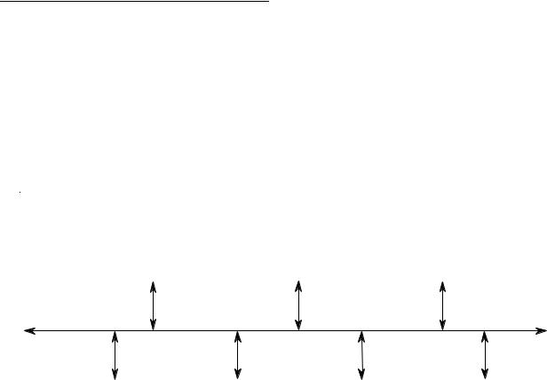
General Description
Nonmultiplexed Serial Interface (NMSI) Implementing Standard Modem Signals
—SCP for Synchronous Communication
—Two Serial Management Controllers (SMCs) To Support IDL and GCI Auxiliary
Channels
1.3 MC68302 SYSTEM ARCHITECTURE
Most general-purpose microprocessor-based systems use an architecture that interfaces all peripheral devices directly onto a single microprocessor bus (see Figure 1-2).
CPU |
|
ROM |
|
RAM |
|
|
|
|
|
SYSTEM BUS
|
|
DMA AND/ |
|
CPU I/F |
|
|
|
|
OR FIFOs |
|
|
|
|
|
|
|
|
|
ADDITIONAL |
|
DMA |
|
|
|
|
|
|
|
|
|
|
|||
|
|
|
|
|
DEVICES |
|
|
|
SERIAL |
|
|
|
|
|
|
|
TIMERS |
|
|
|
|
|
CHANNELS |
|
|
|
|
|
|
|
|
|
|
|
|
|
|
|
|
|
|
Figure 1-2. General-Purpose Microprocessor System Design
The MC68302 microprocessor architecture is shown in Figure 1-3. In this architecture, the peripheral devices are isolated from the system bus through a dual-port memory. Various parameters and counters and all memory buffer descriptor tables reside in the dual-port RAM. The receive and transmit data buffers may be located in the on-chip RAM or in the offchip system RAM. Six DMA channels are dedicated to the six serial ports (receive and transmit for each of the three SCC channels). If data for an SCC channel is programmed to be located in the external RAM, the CP will program the corresponding DMA channel for the required accesses, bypassing the dual-port RAM. If data resides in the dual-port RAM, then the CP accesses the RAM with one clock cycle and no arbitration delays.
1-4 |
MC68302 USER’S MANUAL |
MOTOROLA |
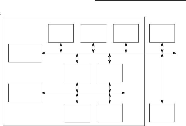
General Description
|
|
|
MC68302 IMP |
|
|
|
1 GENERAL- |
3 TIMERS |
|
INTERRUPT |
|
PURPOSE |
AND |
RAM / ROM |
CONTROLLER |
|
DMA |
ADDITIONAL |
|
|
|
|||
|
|
CHANNEL |
FEATURES |
|
|
|
68000 |
|
|
M68000 |
|
SYSTEM BUS |
|
|
CORE |
|
|
|
|
|
6 DMA |
1152 BYTES |
|
|
|
DUAL-PORT |
|
|
|
|
CHANNELS |
|
|
|
|
RAM |
|
|
|
|
|
|
|
|
MICROCODED |
PERIPHERAL BUS |
|
|
|
COMMUNICATIONS |
|
|
||
CONTROLLER |
|
|
|
|
(RISC) |
|
|
|
|
|
3 SERIAL |
OTHER |
|
OTHER |
|
SERIAL |
|
||
|
CHANNELS |
|
PERIPHERALS |
|
|
CHANNELS |
|
||
|
|
|
|
|
Figure 1-3. MC68302 System Design
The use of a unique arbitration scheme and synchronous transfers between the microprocessor and dual-port RAM gives zero wait-state operation to the M68000 microprocessor core. The dual-port RAM can be accessed by the CP main controller (RISC) once every clock cycle for either read or write operations. When the M68000 core accesses the dualport RAM, each access is pipelined along with the CP accesses so that data is read or written without conflict. The net effect is the loss of a single memory access by the CP main controller per M68000 core access.
The buffer memory structure of the MC68302 can be configured to closely match I/O channel requirements by careful selection of buffer size and buffer linking. The interrupt structure is also programmable so that the on-chip M68000 processor can be off-loaded from the peripheral bit-handling functions to perform higher layer application software or protocol processing.
1.4 NMSI COMMUNICATIONS-ORIENTED ENVIRONMENT
When the interface to equipment or proprietary networks requires the use of standard control and data signals, the MC68302 can be programmed into the nonmultiplexed serial interface (NMSI) mode. This mode, which is available for one, two, or all three SCC ports, can be selected while the other ports use one of the multiplexed interface modes (IDL, GCI, or PCM highway).
MOTOROLA |
MC68302 USER’S MANUAL |
1-5 |

General Description
In the example shown in Figure 1-4, one SCC channel connects through the NMSI mode to a commercial packet data network. This connection might be used for remote status monitoring or for maintenance functions for a system. Another SCC is used to connect to a local asynchronous terminal. The other SCC channel is used as a local synchronous channel, which could connect to another computer or subsystem. The SCP channel could then be used for local interconnection of interface chips or peripherals to the MC68302-based system.
1.5 BASIC RATE ISDN OR DIGITAL VOICE/DATA TERMINAL
A basic rate ISDN (2B + D) or digital voice/data terminal can be made from a chip set based on the MC68302. Refer to Figure 1-5 for an example of a basic rate ISDN voice/data terminal. In this terminal, the CP can directly support the 2B + D channels and perform either
V.110 or V.120 rate adaption. The physical layer serial interface is connected to the local interconnection bus (IDL in Figure 1-5, but the GCI and PCM buses can also be supported).
The system then supports one of the B channels for voice (connected directly to the physical bus). The D channel consists of one SCC port; the other B channel is used for data transfer through a second SCC port. The data can be routed to a terminal (RS-232 type) via the third SCC port in the NMSI mode. The SCP functions as a control channel for the IDL bus in this case.
Some ISDN physical layer devices support the signaling and framing functions of the D channel. In these cases, the D channel can connect through the microprocessor interface to the physical layer device, and the extra SCC port can then be used for a second B channel to transfer data.
The benefit of a local interconnection bus (see Figure 1-5) versus a microprocessor bus is a lower pin count. It is also easy to maintain this low pin-count interface between several different interface chips, such as the MC145554 PCM codec/filter monocircuit and the MC145474 S/T transceiver.
The MC68302 combines the M68000 architecture with a number of peripherals for integrated applications in communications control. The M68000 core manages the CP through the on-chip, dual-port RAM and internal registers. The base address of the dual-port RAM and internal registers is selected through the base address register. Other peripherals are also accessed and controlled through internal registers: the IDMA controller, the three timers, I/O ports, and the interrupt controller.
1-6 |
MC68302 USER’S MANUAL |
MOTOROLA |
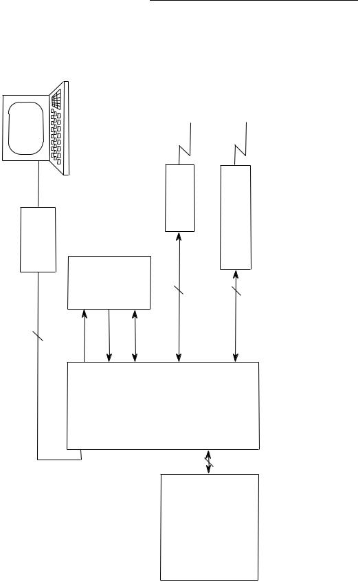
General Description
X.25 WIDE AREA NETWORK (E.G., REMOTE STATUS REPORTS)
|
|
|
|
|
MODEM |
RS232 |
DRIVER |
|
|
|
|
|
|
PROGRAM ROM |
|
|
7 |
NMSIINTERFACE7 |
ADDRESS |
DATA |
CONTROL |
MC68302 IMP |
NMSIINTERFACE SCC |
|
SCC |
|
|
|
SCP |
|
|
|
|
|
3 |
LOCAL SYNCHRONOUS CONNECTION (E.G., COMPUTER TO COMPUTER INTERCONNECT)
SCC DRIVER/RECEIVERS
NMSI INTERFACE 4 LOCAL
OTHER CIRCUIT BOARDS, VLSI, OR EXTERNAL SENSORS ––––– LOCAL SERIAL PORT
Figure 1-4. NMSI Communications-Oriented Board Design
MOTOROLA |
MC68302 USER’S MANUAL |
1-7 |
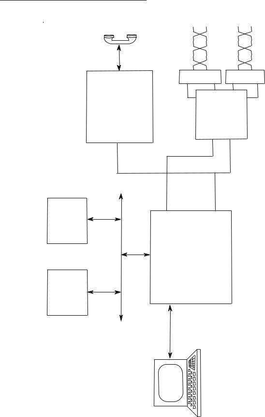
General Description
POTS |
|
|
WIRE |
|
|
|
|
FOUR |
|
MC145554 PCM CODEC/FILTER MONOCIRCUIT |
|
|
MC145474 S/T |
TRANSCEIVER |
|
|
ICL |
(CONTROL) |
B1+B2+D |
B1 |
|
|
|
|
|
|
IDL (DATA) |
B2+D |
|
EPROM |
SCP |
SCC |
SCC |
|
BUSM68000 |
M68000/DMA/CS |
MC68302 IMP |
|
|
RAM |
SCC |
|
|
|
|
ASYNCHRONOUS/ BISYNC/ |
DDCMP |
|
|
Figure 1-5. Basic Rate IDL Voice/Data Terminal in ISDN
1-8 |
MC68302 USER’S MANUAL |
MOTOROLA |
 Loading...