


Motorola MC34160DW, MC34160DWR2, MC34160P, MC33160DW, MC33160DWR2 Datasheet
...
Microprocessor
Voltage Regulator and
Supervisory Circuit
The MC34160 Series is a voltage regulator and supervisory circuit containing many of the necessary monitoring functions required in microprocessor based systems. It is specifically designed for appliance and industrial applications, offering the designer a cost effective solution with minimal external components. These integrated circuits feature a 5.0 V/100 mA regulator with short circuit current limiting, pinned out 2.6 V bandgap reference, low voltage reset comparator, power warning comparator with programmable hysteresis, and an uncommitted comparator ideally suited for microprocessor line synchronization.
Additional features include a chip disable input for low standby current, and internal thermal shutdown for over temperature protection.
These devices are contained in a 16 pin dual±in±line heat tab plastic package for improved thermal conduction.
•5.0 V Regulator Output Current in Excess of 100 mA
•Internal Short Circuit Current Limiting
•Pinned Out 2.6 V Reference
•Low Voltage Reset Comparator
•Power Warning Comparator with Programmable Hysteresis
•Uncommitted Comparator
•Low Standby Current
•Internal Thermal Shutdown Protection
•Heat Tab Power Package
|
Representative Block Diagram |
|
||||
VCC |
+ |
|
|
|
|
Regulator |
|
|
|
|
Output |
||
14 |
|
|
|
0.913 R |
|
11 |
|
|
|
Thermal |
|
Reset |
|
|
|
|
|
+ |
||
|
|
|
Shutdown |
0.01 R |
||
|
|
|
± |
7 |
||
|
|
|
± |
|||
|
|
|
R |
|
Reference |
|
|
|
|
+ |
|
||
Chip Disable |
|
|
|
|
Output |
|
2.6 V |
|
|
|
|
||
15 |
|
|
|
|
16 |
|
Reference |
|
+ |
|
|
||
|
|
|
|
Power |
||
Power |
|
|
|
|
||
|
|
|
|
|
||
|
|
|
± |
|
Warning |
|
Sense |
|
|
|
|
||
|
|
|
+ |
|
8 |
|
9 |
|
|
|
|
||
|
|
|
|
|
||
Hysteresis |
|
IH |
|
|
|
|
Adjust |
|
IH On/Off |
|
|
|
|
10 |
|
|
|
|
|
|
Noninverting |
|
|
|
|
|
|
Input |
|
|
|
|
|
|
2 |
+ |
|
|
|
|
Comparator |
Inverting |
|
|
|
|
||
|
|
+ |
|
|
Output |
|
Input |
|
|
|
|
||
|
|
|
|
6 |
||
1 |
|
|
± |
|
|
|
|
|
|
|
|
||
Gnd  4, 5, 12, 13
This device contains 72 active transistors.
Order this document by MC34160/D
MC34160
MC33160
MICROPROCESSOR
VOLTAGE REGULATOR/
SUPERVISORY CIRCUIT
SEMICONDUCTOR
TECHNICAL DATA
16
1
P SUFFIX
PLASTIC PACKAGE
CASE 648C (DIP±16)
16
1
DW SUFFIX
PLASTIC PACKAGE
CASE 751G
(SOP±16L)
PIN CONNECTIONS
|
|
|
|
|
|
|
|
|
|
|
|
Comp. Inv. In |
1 |
|
|
|
|
16 |
Vref |
||||
|
|
|
|
|
|
|
|
|
|
||
Comp. Noninv. In |
2 |
|
|
|
|
15 |
Chip Disable |
||||
|
|
|
|
|
|
|
|
|
|
|
|
|
N.C. |
3 |
|
|
|
|
14 |
VCC |
|||
|
|
|
|
|
|
|
|
|
|
|
|
Gnd |
|
|
4 |
|
|
|
|
13 |
|
Gnd |
|
|
|
|
|
|
|
|
|
||||
|
|
|
|
5 |
|
|
|
|
12 |
|
|
|
|
|
|
|
|
|
|
|
|
|
|
|
|
|
|
|
|
|
|
|
|
||
Comp. Out |
6 |
|
|
|
|
11 |
Reg. Out |
||||
|
|
|
|
|
|
|
|
|
|
|
|
|
Reset |
7 |
|
|
|
|
10 |
Hyst. Adj. |
|||
|
|
|
|
|
|
|
|
|
|
||
Power Warning |
8 |
|
|
|
|
9 |
Power Sense |
||||
|
|
|
|
|
|
|
|
|
|
|
|
|
|
|
|
|
|
(Top View) |
|
|
|||
ORDERING INFORMATION
|
Operating |
|
|
Device |
Temperature Range |
Package |
|
|
|
|
|
MC34160DW |
TA = 0° to +70°C |
SOP±16L |
|
|
|
||
MC34160P |
DIP±16 |
||
|
|||
|
|
|
|
MC33160DW |
TA = ± 40° to +85°C |
SOP±16L |
|
|
|
||
MC33160P |
DIP±16 |
||
|
|||
|
|
|
Motorola, Inc. 1996 |
Rev 1 |

MC34160 MC33160
MAXIMUM RATINGS
Rating |
Symbol |
Value |
Unit |
|
|
|
|
Power Supply Voltage |
VCC |
40 |
V |
Chip Disable Input Voltage (Pin 15, Note 1) |
VCD |
±0.3 to VCC |
V |
Comparator Input Current (Pins 1, 2, 9) |
Iin |
±2.0 to +2.0 |
mA |
Comparator Output Voltage (Pins 6, 7, 8) |
VO |
40 |
V |
Comparator Output Sink Current (Pins 6, 7, 8) |
ISink |
10 |
mA |
Power Dissipation and Thermal Characteristics |
|
|
°C/W |
P Suffix, Dual±In±Line Case 648C |
|
|
|
Thermal Resistance, Junction±to±Air |
RθJA |
80 |
|
Thermal Resistance, Junction±to±Case (Pins 4, 5, 12, 13) |
RθJC |
15 |
|
DW Suffix, Surface Mount Case 751G |
|
|
|
Thermal Resistance, Junction±to±Air |
RθJA |
94 |
|
Thermal Resistance, Junction±to±Case (Pins 4, 5, 12, 13) |
RθJC |
18 |
|
Operating Junction Temperature |
TJ |
+150 |
°C |
Operating Ambient Temperature |
TA |
|
°C |
MC34160 |
|
0 to +70 |
|
MC33160 |
|
±40 to +85 |
|
|
|
|
|
Storage Temperature Range |
Tstg |
±65 to +150 |
°C |
ELECTRICAL CHARACTERISTICS (VCC = 30 V, IO = 10 mA, Iref = 100 μA) For typical values TA = 25°C, for min/max values TA is the operating ambient temperature range that applies [Notes 2 and 3], unless otherwise noted.)
Characteristics |
Symbol |
Min |
Typ |
Max |
Unit |
||
|
|
|
|
|
|
|
|
REGULATOR SECTION |
|
|
|
|
|
|
|
|
|
|
|
|
|
|
|
Total Output Variation (VCC = 7.0 V to 40 V, |
|
VO |
4.75 |
5.0 |
5.25 |
V |
|
IO = 1.0 mA to 100 mA, TA = Tlow to Thigh) |
|
|
|
|
|
||
Line Regulation (VCC = 7.0 V to 40 V, TA = 25°C) |
Regline |
± |
5.0 |
40 |
mV |
||
Load Regulation (IO = 1.0 V to 100 mA, TA = 25°C) |
Regload |
± |
20 |
50 |
mV |
||
Ripple Rejection |
|
|
RR |
50 |
6.5 |
± |
dB |
(VCC = 25 V to 35 V, IO = 40 mA, f = 120 Hz, TA = 25°C) |
|
|
|
|
|
||
REFERENCE SECTION |
|
|
|
|
|
|
|
|
|
|
|
|
|
|
|
Total Output Variation (VCC = 7.0 to 40 V, |
|
Vref |
2.47 |
2.6 |
2.73 |
V |
|
IO = 0.1 mA to 2.0 mA, TA = Tlow to Thigh) |
|
|
|
|
|
||
Line Regulation (VCC = 5.0 V to 40 V, TA = 25°C) |
Regline |
± |
2.0 |
20 |
mV |
||
Load Regulation (IO = 0.1 mA to 2.0 mA, TA = 25°C) |
Regload |
± |
4.0 |
30 |
mV |
||
RESET COMPARATOR |
|
|
|
|
|
|
|
|
|
|
|
|
|
|
|
Threshold Voltage |
|
|
|
|
|
|
V |
High State Output (Pin 11 Increasing) |
|
VIH |
± |
(VO±0.11) |
(VO±0.05) |
|
|
Low State Output (Pin 11 Decreasing) |
|
VIL |
4.55 |
(VO±0.18) |
± |
|
|
Hysteresis |
|
|
VH |
0.02 |
0.07 |
± |
|
Output Sink Saturation (VCC = 4.5 V, ISink = 2.0 mA) |
VOL |
± |
± |
0.4 |
V |
||
Output Off±State Leakage (VOH = 40 V) |
|
IOH |
± |
± |
4.0 |
μA |
|
NOTES: 1. The maximum voltage range is ±0.3 V to VCC or +35 V, whichever is less. |
|
|
|
|
|
||
2. Tlow = 0°C for MC34160 |
Thigh |
= 70°C for MC34160 |
|
|
|
|
|
±40°C for MC33160 |
|
85°C for MC33160 |
|
|
|
|
|
3. Low duty cycle pulse testing techniques are used during test to maintain junction temperature as close to ambient as possible.
2 |
MOTOROLA ANALOG IC DEVICE DATA |
MC34160 MC33160
ELECTRICAL CHARACTERISTICS (continued) (VCC = 30 V, IO = 10 mA, Iref = 100 μA) For typical values TA = 25°C, for min/max values TA is the operating ambient temperature range that applies [Notes 2 and 3], unless otherwise noted.)
Characteristics |
Symbol |
Min |
Typ |
Max |
Unit |
||
|
|
|
|
|
|
|
|
POWER WARNING COMPARATOR |
|
|
|
|
|
|
|
|
|
|
|
|
|
|
|
Input Offset Voltage |
|
|
VIO |
± |
1.2 |
10 |
mV |
Input Bias Current (VPin 9 = 3.0 V) |
|
|
IIB |
± |
± |
0.5 |
μA |
Input Hysteresis Current (VPin 9 = Vref ± 100 mV) |
IH |
|
|
|
μA |
||
RPin 10 = 24 k |
|
|
|
40 |
50 |
60 |
|
RPin 10 = ∞ |
|
|
|
4.5 |
7.5 |
11 |
|
Output Sink Saturation (ISink = 2.0 mA) |
|
VOL |
± |
0.13 |
0.4 |
V |
|
Output Off±State Leakage (VOH = 40 V) |
|
IOH |
± |
± |
4.0 |
μA |
|
UNCOMMITTED COMPARATOR |
|
|
|
|
|
|
|
|
|
|
|
|
|
||
Input Offset Voltage (Output Transition Low to High) |
VIO |
± |
± |
20 |
mV |
||
Input Hysteresis Voltage (Output Transition High to Low) |
IH |
140 |
200 |
260 |
mV |
||
Input Bias Current (VPin 1, 2 = 2.6 V) |
|
|
IIB |
± |
± |
±1.0 |
μA |
Input Common Mode Voltage Range |
|
|
VICR |
0.6 to 5.0 |
± |
± |
V |
Output Sink Saturation (ISink = 2.0 mA) |
|
VOL |
± |
0.13 |
0.4 |
V |
|
Output Off±State Leakage (VOH = 40 V) |
|
IOH |
± |
± |
4.0 |
μA |
|
TOTAL DEVICE |
|
|
|
|
|
|
|
|
|
|
|
|
|
|
|
Chip Disable Threshold Voltage (Pin 15) |
|
|
|
|
|
V |
|
High State (Chip Disabled) |
|
|
VIH |
2.5 |
± |
± |
|
Low State (Chip Enabled) |
|
|
VIL |
± |
± |
0.8 |
|
Chip Disable Input Current (Pin 15) |
|
|
|
|
|
|
μA |
High State (Vin = 2.5 V) |
|
|
IIH |
± |
± |
100 |
|
Low State (Vin = 0.8 V) |
|
|
IIL |
± |
± |
30 |
|
Chip Disable Input Resistance (Pin 15) |
|
Rin |
50 |
100 |
± |
kΩ |
|
Operating Voltage Range |
|
|
VCC |
|
|
|
V |
VO (Pin 11) Regulated |
|
|
|
7.0 to 40 |
± |
± |
|
Vref (Pin 16) Regulated |
|
|
|
5.0 to 40 |
± |
± |
|
Power Supply Current |
|
|
ICC |
|
|
|
mA |
Standby (Chip Disable High State) |
|
|
|
± |
0.18 |
0.35 |
|
Operating (Chip Disable Low State) |
|
|
|
± |
1.5 |
3.0 |
|
|
|
|
|
|
|
||
NOTES: 1. The maximum voltage range is ±0.3 V to VCC or +35 V, whichever is less. |
|
|
|
|
|
||
2. Tlow = 0°C for MC34160 |
Thigh |
= 70°C for MC34160 |
|
|
|
|
|
±40°C for MC33160 |
|
85°C for MC33160 |
|
|
|
|
|
3. Low duty cycle pulse testing techniques are used during test to maintain junction temperature as close to ambient as possible.
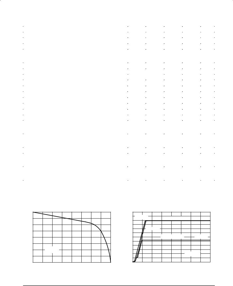
VO, REGULATOR OUTPUT VOLTAGE CHANGE (mV)
Figure 1. Regulator Output Voltage Change
versus Source Current
0
±4.0 |
|
|
|
±8.0 |
|
|
|
±12 |
VCC = 7.5 V |
|
|
|
TA = 25°C |
|
|
±16 |
|
|
|
0 |
40 |
80 |
120 |
IO, REGULATOR OUTPUT SOURCE CURRENT (mA)
|
|
Figure 2. Reference and Regulator Output |
||||
|
|
|
versus Supply Voltage |
|
|
|
|
|
6.0 |
|
|
|
|
|
|
RL = 1 |
|
Regulator Output |
|
|
|
(V) |
|
|
Reference Output |
|
RL = 1 |
|
VOLTAGE |
|
|
|
||
|
|
4.0 |
RL = 50 Ω |
|
|
|
|
OUTPUT |
2.0 |
|
|
|
|
|
|
|
|
|
|
|
|
|
|
|
TA = 25°C |
||
|
|
0 |
|
|
|
|
160 |
|
0 |
10 |
20 |
30 |
40 |
|
|
|
|
VCC, SUPPLY VOLTAGE (V) |
|
|
MOTOROLA ANALOG IC DEVICE DATA |
3 |
|
 Loading...