


Motorola MC34163DWR2, MC34163P, MC33163P, MC33163DW, MC34163DW Datasheet
...Order this document by MC34163/D
Power Switching Regulators
The MC34163 series are monolithic power switching regulators that contain the primary functions required for dc±to±dc converters. This series is specifically designed to be incorporated in step±up, step±down, and voltage±inverting applications with a minimum number of external components.
These devices consist of two high gain voltage feedback comparators, temperature compensated reference, controlled duty cycle oscillator, driver with bootstrap capability for increased efficiency, and a high current output switch. Protective features consist of cycle±by±cycle current limiting, and internal thermal shutdown. Also included is a low voltage indicator output designed to interface with microprocessor based systems.
These devices are contained in a 16 pin dual±in±line heat tab plastic package for improved thermal conduction.
•Output Switch Current in Excess of 3.0 A
•Operation from 2.5 V to 40 V Input
•Low Standby Current
•Precision 2% Reference
•Controlled Duty Cycle Oscillator
•Driver with Bootstrap Capability for Increased Efficiency
•Cycle±by±Cycle Current Limiting
•Internal Thermal Shutdown Protection
•Low Voltage Indicator Output for Direct Microprocessor Interface
•Heat Tab Power Package
Representative Block Diagram
I |
pk |
Sense |
8 |
± |
ILimit |
|
9 |
Driver |
|
Collector |
|||||||
|
|
|
|
|
|
|
||
|
|
|
|
|
|
|
|
|
|
|
|
|
+ |
|
|
|
|
|
|
VCC |
7 |
+ |
|
|
10 |
Switch |
|
|
|
|
|
|
|
||
|
|
Timing |
|
|
|
|
|
Collector |
|
|
6 |
OSC |
|
|
11 |
|
|
Capacitor |
|
|
|
|||||
|
|
|
|
|
|
|||
|
|
|
5 |
Control Logic |
|
12 |
|
|
|
|
|
|
|
|
Gnd |
||
|
Gnd |
|
and Thermal |
|
|
|||
|
|
|
4 |
Shutdown |
|
13 |
|
|
|
|
|
|
|
+ |
|
||
|
|
|
|
|
|
|
|
|
|
Voltage |
3 |
|
|
|
14 |
|
|
Feedback 1 |
|
|
|
|
||||
|
|
|
|
|
Switch |
|||
|
|
|
|
|
|
|
|
|
|
Voltage |
|
|
VFB |
|
|
Emitter |
|
|
2 |
|
+ |
|
15 |
|
||
Feedback 2 |
|
+ |
|
|
||||
|
|
|
|
|
||||
|
|
|
|
|
± |
|
|
|
|
|
|
|
LVI |
|
|
|
Bootstrap |
LVI Output |
1 |
+ |
|
|
16 |
|||
+ |
|
|
Input |
|||||
|
|
|
|
± |
|
|
|
|
|
|
|
|
|
|
|
+ |
|
(Bottom View)
This device contains 114 active transistors.
MC34163
MC33163
POWER SWITCHING
REGULATORS
SEMICONDUCTOR
TECHNICAL DATA
16
1
P SUFFIX
PLASTIC PACKAGE
CASE 648C
(DIP±16)
16
1
DW SUFFIX
PLASTIC PACKAGE
CASE 751G
(SOP±16L)
PIN CONNECTIONS
|
|
|
|
|
|
|
Bootstrap Input |
LVI Output |
1 |
|
|
|
|
16 |
|
Voltage Feedback 2 |
|
|
|
|
|
|
|
2 |
|
|
|
|
15 |
Switch |
|
|
|
|
|
|
|
|
|
Voltage Feedback 1 |
|
|
|
|
|
|
Emitter |
3 |
|
|
|
|
14 |
||
|
|
|
|
|
|||
|
|
|
|
|
|
|
|
|
|
|
|
|
|
|
|
Gnd |
4 |
|
|
|
|
13 |
Gnd |
|
|
|
|
|
|
||
|
|
|
|
|
|
||
|
5 |
|
|
|
|
12 |
|
Timing Capacitor |
|
|
|
|
|
|
|
|
|
|
|
|
|
|
|
6 |
|
|
|
|
11 |
|
|
VCC |
|
|
|
|
|
|
Switch Collector |
|
|
|
|
|
|
||
7 |
|
|
|
|
10 |
||
|
|
|
|
|
|||
Ipk Sense |
|
|
|
|
|
|
Driver Collector |
8 |
|
|
|
|
9 |
||
|
|
|
|
|
|
|
|
(Top View)
ORDERING INFORMATION
|
Operating |
|
|
Device |
Temperature Range |
Package |
|
|
|
|
|
MC34163DW |
TA = 0° to +70°C |
SOP±16L |
|
|
|
||
MC34163P |
DIP±16 |
||
|
|||
|
|
|
|
MC33163DW |
TA = ± 40° to +85°C |
SOP±16L |
|
|
|
||
MC33163P |
DIP±16 |
||
|
|||
|
|
|
Motorola, Inc. 1996 |
Rev 2 |

MC34163 MC33163
MAXIMUM RATINGS
Rating |
Symbol |
Value |
Unit |
|
|
|
|
Power Supply Voltage |
VCC |
40 |
V |
Switch Collector Voltage Range |
VC(switch) |
±1.0 to + 40 |
V |
Switch Emitter Voltage Range |
VE(switch) |
± 2.0 to VC(switch) |
V |
Switch Collector to Emitter Voltage |
VCE(switch) |
40 |
V |
Switch Current (Note 1) |
ISW |
3.4 |
A |
Driver Collector Voltage |
VC(driver) |
±1.0 to +40 |
V |
Driver Collector Current |
IC(driver) |
150 |
mA |
Bootstrap Input Current Range (Note 1) |
IBS |
±100 to +100 |
mA |
Current Sense Input Voltage Range |
VIpk (Sense) |
(VCC±7.0) to (VCC+1.0) |
V |
Feedback and Timing Capacitor Input |
Vin |
±1.0 to + 7.0 |
V |
Voltage Range |
|
|
|
|
|
|
|
Low Voltage Indicator Output Voltage |
VC(LVI) |
±1.0 to + 40 |
V |
Range |
|
|
|
|
|
|
|
Low Voltage Indicator Output Sink Current |
IC(LVI) |
10 |
mA |
Thermal Characteristics |
|
|
°C/W |
P Suffix, Dual±In±Line Case 648C |
|
|
|
Thermal Resistance, Junction±to±Air |
RθJA |
80 |
|
Thermal Resistance, Junction±to±Case |
RθJC |
15 |
|
(Pins 4, 5, 12, 13) |
|
|
|
DW Suffix, Surface Mount Case 751G |
|
|
|
Thermal Resistance, Junction±to±Air |
RθJA |
94 |
|
Thermal Resistance, Junction±to±Case |
RθJC |
18 |
|
(Pins 4, 5, 12, 13) |
|
|
|
|
|
|
|
Operating Junction Temperature |
TJ |
+150 |
°C |
Operating Ambient Temperature (Note 3) |
TA |
|
°C |
MC34163 |
|
0 to +70 |
|
MC33163 |
|
± 40 to + 85 |
|
|
|
|
|
Storage Temperature Range |
Tstg |
± 65 to +150 |
°C |
ELECTRICAL CHARACTERISTICS (VCC = 15 V, Pin 16 = VCC, CT = 620 pF, for typical values TA = 25°C, for min/max values TA is the operating ambient temperature range that applies (Note 3), unless otherwise noted.)
Characteristic |
|
Symbol |
Min |
Typ |
Max |
Unit |
|
|
|
|
|
|
|
|
|
OSCILLATOR |
|
|
|
|
|
|
|
|
|
|
|
|
|
|
|
Frequency |
|
|
fOSC |
|
|
|
kHz |
TA = 25°C |
|
|
|
46 |
50 |
54 |
|
Total Variation over VCC = 2.5 V to 40 V, and Temperature |
|
45 |
± |
55 |
|
||
Charge Current |
|
|
Ichg |
± |
225 |
± |
μA |
Discharge Current |
|
|
Idischg |
± |
25 |
± |
μA |
Charge to Discharge Current Ratio |
|
|
Ichg/Idischg |
8.0 |
9.0 |
10 |
± |
Sawtooth Peak Voltage |
|
|
VOSC(P) |
± |
1.25 |
± |
V |
Sawtooth Valley Voltage |
|
|
VOSC(V) |
± |
0.55 |
± |
V |
FEEDBACK COMPARATOR 1 |
|
|
|
|
|
|
|
|
|
|
|
|
|
|
|
Threshold Voltage |
|
|
Vth(FB1) |
|
|
|
|
TA = 25°C |
|
|
|
4.9 |
5.05 |
5.2 |
V |
Line Regulation (VCC = 2.5 V to 40 V, TA = 25°C) |
|
± |
0.008 |
0.03 |
%/V |
||
Total Variation over Line, and Temperature |
|
|
4.85 |
± |
5.25 |
V |
|
|
|
|
|
|
|
|
|
Input Bias Current (VFB1 = 5.05 V) |
|
|
IIB(FB1) |
± |
100 |
200 |
μA |
NOTES: 1. Maximum package power dissipation limits must be observed. |
|
|
|
|
|
||
2. Low duty cycle pulse techniques are used during test to maintain junction temperature as close to ambient as possible. |
|
|
|||||
3. Tlow = 0°C for MC34163 |
Thigh |
= + 70°C for MC34163 |
|
|
|
|
|
= ± 40°C for MC33163 |
|
= + 85°C for MC33163 |
|
|
|
|
|
2 |
MOTOROLA ANALOG IC DEVICE DATA |
MC34163 MC33163
ELECTRICAL CHARACTERISTICS (continued) (VCC = 15 V, Pin 16 = VCC, CT = 620 pF, for typical values TA = 25°C, for min/max values TA is the operating ambient temperature range that applies (Note 3), unless otherwise noted.)
Characteristic |
|
Symbol |
Min |
Typ |
Max |
Unit |
|
|
|
|
|
|
|
|
|
FEEDBACK COMPARATOR 2 |
|
|
|
|
|
|
|
|
|
|
|
|
|
|
|
Threshold Voltage |
|
|
Vth(FB2) |
|
|
|
|
TA = 25°C |
|
|
|
1.225 |
1.25 |
1.275 |
V |
Line Regulation (VCC = 2.5 V to 40 V, TA = 25°C) |
|
± |
0.008 |
0.03 |
%/V |
||
Total Variation over Line, and Temperature |
|
|
1.213 |
± |
1.287 |
V |
|
|
|
|
|
|
|
|
|
Input Bias Current (VFB2 = 1.25 V) |
|
|
IIB(FB2) |
± 0.4 |
0 |
0.4 |
μA |
CURRENT LIMIT COMPARATOR |
|
|
|
|
|
|
|
|
|
|
|
|
|
|
|
Threshold Voltage |
|
|
Vth(Ipk Sense) |
|
|
|
mV |
TA = 25°C |
|
|
|
± |
250 |
± |
|
Total Variation over VCC = 2.5 V to 40 V, and Temperature |
|
230 |
± |
270 |
|
||
Input Bias Current (VIpk (Sense) = 15 V) |
|
IIB(sense) |
± |
1.0 |
20 |
μA |
|
DRIVER AND OUTPUT SWITCH (Note 2) |
|
|
|
|
|
|
|
|
|
|
|
|
|
||
Sink Saturation Voltage (ISW = 2.5 A, Pins 14, 15 grounded) |
VCE(sat) |
|
|
|
V |
||
Non±Darlington Connection (RPin 9 = 110 Ω to VCC, ISW/IDRV ≈ 20) |
|
± |
0.6 |
1.0 |
|
||
Darlington Connection (Pins 9, 10, 11 connected) |
|
± |
1.0 |
1.4 |
|
||
|
|
|
|
|
|
||
Collector Off±State Leakage Current (VCE = 40 V) |
IC(off) |
± |
0.02 |
100 |
μA |
||
Bootstrap Input Current Source (VBS = VCC + 5.0 V) |
Isource(DRV) |
0.5 |
2.0 |
4.0 |
mA |
||
Bootstrap Input Zener Clamp Voltage (IZ = 25 mA) |
VZ |
VCC + 6.0 |
VCC + 7.0 |
VCC + 9.0 |
V |
||
LOW VOLTAGE INDICATOR |
|
|
|
|
|
|
|
|
|
|
|
|
|
|
|
Input Threshold (VFB2 Increasing) |
|
|
Vth |
1.07 |
1.125 |
1.18 |
V |
Input Hysteresis (VFB2 Decreasing) |
|
|
VH |
± |
15 |
± |
mV |
Output Sink Saturation Voltage (Isink = 2.0 mA) |
VOL(LVI) |
± |
0.15 |
0.4 |
V |
||
Output Off±State Leakage Current (VOH = 15 V) |
IOH |
± |
0.01 |
5.0 |
μA |
||
TOTAL DEVICE |
|
|
|
|
|
|
|
|
|
|
|
|
|
||
Standby Supply Current (VCC = 2.5 V to 40 V, Pin 8 = VCC, |
ICC |
± |
6.0 |
10 |
mA |
||
Pins 6, 14, 15 = Gnd, remaining pins open) |
|
|
|
|
|
||
|
|
|
|
|
|
||
NOTES: 1. Maximum package power dissipation limits must be observed. |
|
|
|
|
|
||
2. Low duty cycle pulse techniques are used during test to maintain junction temperature as close to ambient as possible. |
|
|
|||||
3. Tlow = 0°C for MC34163 |
Thigh |
= + 70°C for MC34163 |
|
|
|
|
|
= ± 40°C for MC33163 |
|
= + 85°C for MC33163 |
|
|
|
|
|
|
|
|
|
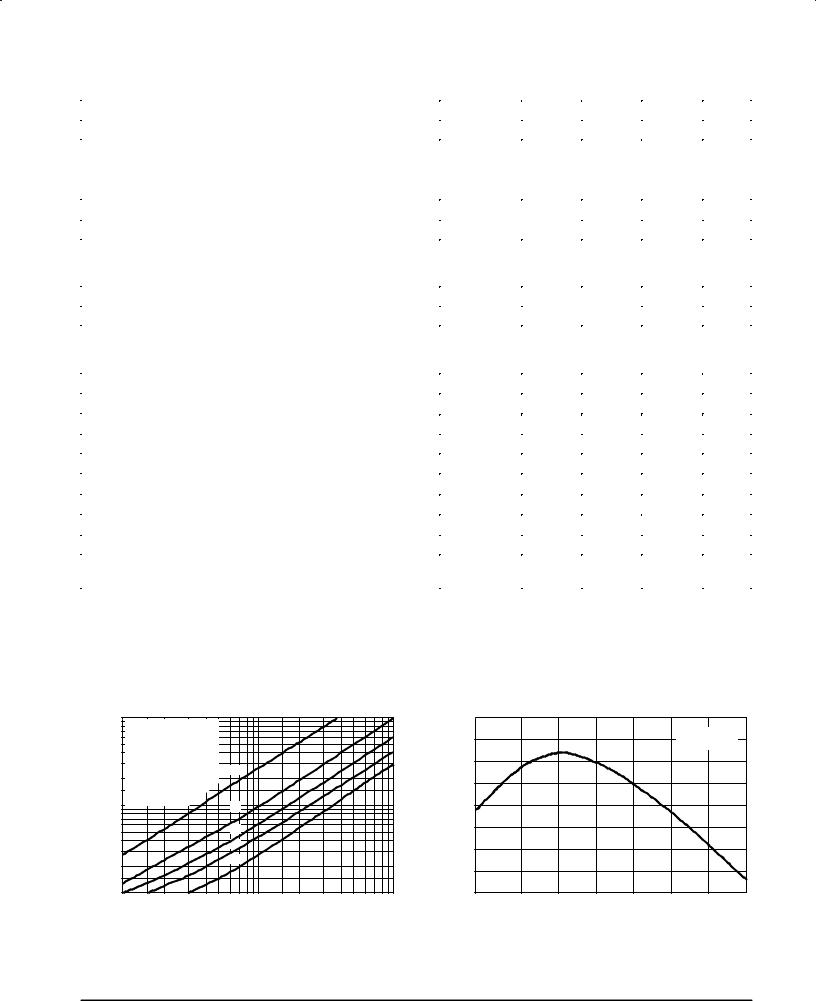
Figure 1. Output Switch On±Off Time |
|
|
s) |
100 |
|
|
versus Oscillator Timing Capacitor |
|
|
(μ |
V |
|
= 15 V |
|
|
|
TIME |
|
|
|
|||
|
CC |
|
|
|
||
|
TA = 25°C |
|
|
|||
ON±OFF |
|
1) |
ton, RDT = ∞ |
|
|
|
|
2) |
ton, RDT = 20 k |
1 |
|
||
|
3) |
ton, toff, RDT = 10 k |
|
|||
SWITCH |
|
4) |
toff, RDT = 20 k |
|
|
|
10 |
5) |
toff, RDT = ∞ |
2 |
|
||
|
|
|
|
|||
|
|
|
|
|
|
|
, OUTPUT |
|
|
|
|
3 |
|
|
|
|
|
4 |
|
|
|
|
|
|
5 |
|
|
off |
|
|
|
|
|
|
|
|
|
|
|
|
|
±t |
|
|
|
|
|
|
on |
1.0 |
|
|
|
|
|
t |
|
|
|
1.0 |
10 |
|
|
0.1 |
|
|
|||
CT, OSCILLATOR TIMING CAPACITOR (nF)
|
|
Figure 2. Oscillator Frequency Change |
|
|||||
(%) |
|
|
versus Temperature |
|
|
|||
2.0 |
|
|
|
|
|
|
|
|
CHANGE |
|
|
|
|
|
|
|
|
|
|
|
|
|
|
VCC = 15 V |
|
|
|
|
|
|
|
|
CT = 620 pF |
|
|
0 |
|
|
|
|
|
|
|
|
FREQUENCY |
|
|
|
|
|
|
|
|
± 2.0 |
|
|
|
|
|
|
|
|
|
|
|
|
|
|
|
|
|
, OSCILLATOR |
± 4.0 |
|
|
|
|
|
|
|
|
|
|
|
|
|
|
|
|
OSC |
± 6.0 |
|
|
|
|
|
|
|
f |
± 25 |
0 |
25 |
50 |
75 |
100 |
125 |
|
|
± 55 |
|||||||
|
|
|
TA, AMBIENT TEMPERATURE (°C) |
|
|
|||
MOTOROLA ANALOG IC DEVICE DATA |
3 |
|

MC34163 MC33163
IIB, INPUT BIAS CURRENT (μA)
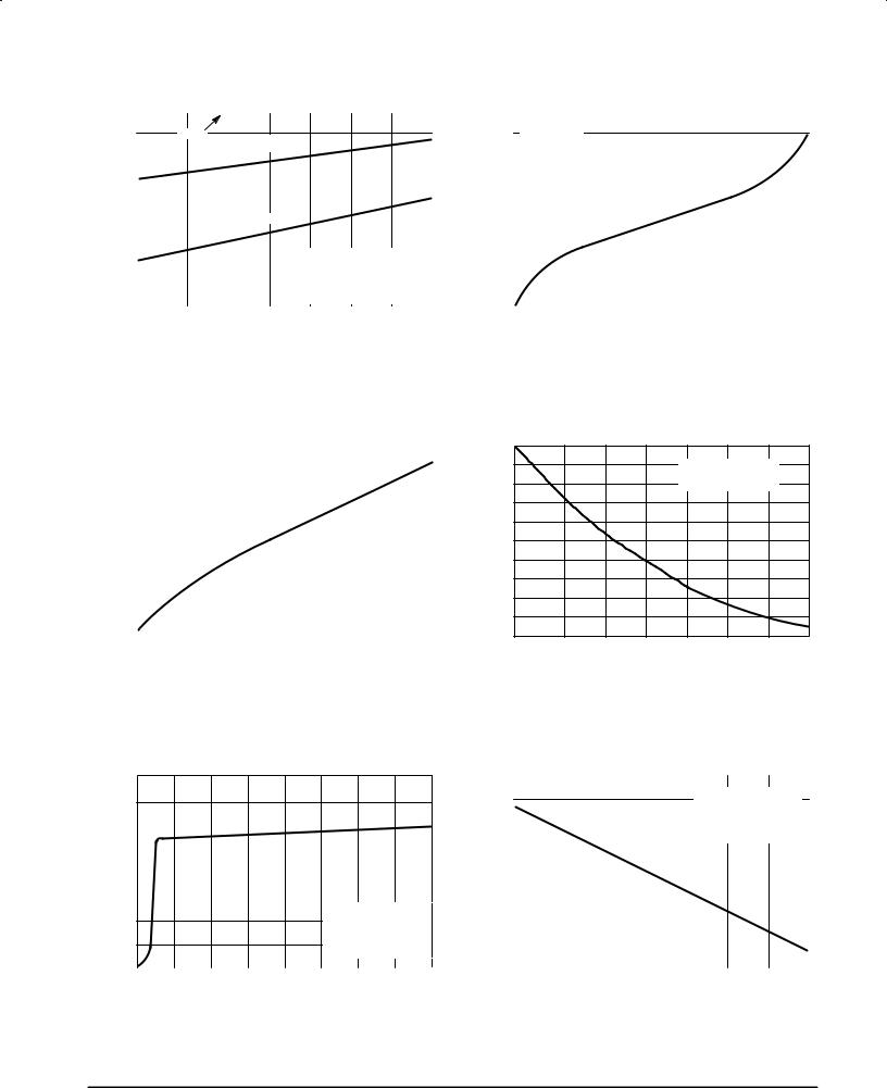
Figure 3. Feedback Comparator 1 Input Bias Current versus Temperature
140
VCC = 15 V
VFB1 = 5.05 V
120
100
80
60 |
± 25 |
0 |
25 |
50 |
75 |
100 |
125 |
± 55 |
TA, AMBIENT TEMPERATURE (°C)
(mV) |
Figure 4. Feedback Comparator 2 Threshold |
Voltage versus Temperature |
VOLTAGE |
1300 |
|
|
|
|
|
|
|
1280 |
VCC = 15 V |
|
|
Vth Max = 1275 mV |
|
|
||
2 THRESHOLD |
|
|
|
|
|
|
|
|
1260 |
|
|
|
Vth Typ = 1250 mV |
|
|
||
|
|
|
|
|
|
|||
|
|
|
|
|
|
|
|
|
, COMPARATOR |
1240 |
|
|
|
|
|
|
|
|
|
|
|
Vth Min = 1225 mV |
|
|
||
1220 |
|
|
|
|
|
|
|
|
|
|
|
|
|
|
|
|
|
th(FB2) |
1200 |
± 25 |
0 |
25 |
50 |
75 |
100 |
125 |
± 55 |
||||||||
V |
|
|
TA, AMBIENT TEMPERATURE (°C) |
|
|
|||
|
|
|
|
|
||||
I source (DRV), BOOTSTRAP INPUT CURRENT SOURCE (mA)
Figure 5. Bootstrap Input Current
Source versus Temperature
2.8
VCC = 15 V
Pin 16 = VCC + 5.0 V
2.4
2.0
1.6
1.2 |
± 25 |
0 |
25 |
50 |
75 |
100 |
125 |
± 55 |
TA, AMBIENT TEMPERATURE (°C)
VZ, BOOTSTRAP INPUT ZENER CLAMP VOLTAGE (V)
Figure 6. Bootstrap Input Zener Clamp
Voltage versus Temperature
7.6
IZ = 25 mA
7.4
7.2
7.0
6.8 |
± 25 |
0 |
25 |
50 |
75 |
100 |
125 |
± 55 |
TA, AMBIENT TEMPERATURE (°C)
VCE (sat), SOURCE SATURATION (V)
0
±0.4
±0.8
±1.2
±1.6
±2.0
0
Figure 7. Output Switch Source Saturation
versus Emitter Current
VCC |
Darlington Configuration |
|
Emitter Sourcing Current to Gnd |
||
|
||
|
Pins 7, 8, 10, 11 = VCC |
|
|
Pins 4, 5, 12, 13 = Gnd |
|
|
TA = 25°C, (Note 2) |
Bootstrapped, Pin 16 = VCC + 5.0 V
Non±Bootstrapped, Pin 16 = VCC
0.8 |
1.6 |
2.4 |
3.2 |
IE, EMITTER CURRENT (A)
VCE (sat), SINK SATURATION (V)
Figure 8. Output Switch Sink Saturation
versus Collector Current
1.2
1.0Darlington, Pins 9, 10, 11 Connected
0.8
Grounded Emitter Configuration
0.6Collector Sinking Current From VCC
|
Pins 7, 8 = VCC = 15 V |
|
0.4 |
Pins 4, 5, 12, 13, 14, 15 = Gnd |
|
TA = 25°C, (Note 2) |
||
|
||
0.2 |
Saturated Switch, RPin9 = 110 Ω to VCC |
|
|
||
|
|
|
0 |
Gnd |
|
|
0 |
0.8 |
1.6 |
2.4 |
3.2 |
|
|
IC, COLLECTOR CURRENT (A) |
|
|
4 |
MOTOROLA ANALOG IC DEVICE DATA |
MC34163 MC33163
Figure 9. Output Switch Negative Emitter
Voltage versus Temperature
|
0 |
|
|
|
|
|
|
|
|
|
|
|
(V) |
|
Gnd |
|
|
IC = 10 |
μA |
|
|
|
|
|
|
± 0.4 |
|
|
|
|
|
|
|
|
||||
|
|
|
|
|
|
|
|
|
||||
|
|
|
|
|
|
|
|
|
|
|
||
|
|
|
|
|
|
|
|
|
|
|
|
|
VOLTAGE |
± 0.8 |
|
|
|
|
|
|
|
|
|
|
|
|
|
|
|
|
|
|
|
|
|
|
||
EMITTER, |
|
|
|
|
|
|
|
|
|
|
|
|
|
|
|
|
|
|
|
|
|
|
|
|
|
± 1.2 |
|
|
|
|
IC = 10 mA |
|
|
|
|
|
||
|
|
|
|
|
|
|
|
|
|
|||
|
|
|
|
|
|
|
|
|
|
|
|
|
|
|
|
|
|
|
|
|
|
|
|
|
|
E |
± 1.6 |
|
|
|
|
|
V |
CC = 15 V |
|
|
|
|
V |
|
|
|
|
|
Pins 7, 8, 9, 10, 16 = VCC |
|
|
||||
|
|
|
|
|
|
|
Pins 4, 6 = Gnd |
|
|
|
||
|
± 2.0 |
|
|
|
|
|
Pin 14 Driven Negative |
|
|
|||
|
|
|
|
|
|
|
|
|
|
|
|
|
|
|
± 25 |
0 |
25 |
50 |
75 |
100 |
125 |
||||
|
± 55 |
|||||||||||
TA, AMBIENT TEMPERATURE (°C)
Figure 11. Current Limit Comparator Threshold
Voltage versus Temperature
(mV) |
254 |
|
VCC = 15 V |
|
|
|
|
|
|
|
|
|
|
|
|
|
VOLTAGE |
252 |
|
|
|
|
|
|
|
|
|
|
|
|
|
|
|
|
|
|
|
|
|
|
|
|
|
|
|
|
|
|
||
THRESHOLD, |
|
|
|
|
|
|
|
|
|
|
|
|
|
|
|
|
250 |
|
|
|
|
|
|
|
|
|
|
|
|
|
|
|
|
|
|
|
|
|
|
|
|
|
|
|
|
|
|
|
||
Sense)(Ipkth |
|
|
|
|
|
|
|
|
|
|
|
|
|
|
|
|
248 |
|
|
|
|
|
|
|
|
|
|
|
|
|
|
|
|
|
|
|
|
|
|
|
|
|
|
|
|
|
|
|
||
|
|
|
|
|
|
|
|
|
|
|
|
|
|
|
|
|
V |
246 |
|
|
|
|
|
|
|
|
|
|
|
|
|
|
|
|
|
|
|
|
|
|
|
|
|
|
|
|
|
|
||
|
|
|
|
|
|
|
|
|
|
|
|
|
|
|
||
|
± 55 |
± 25 |
0 |
25 |
50 |
75 |
100 |
125 |
||||||||
|
|
|
|
|
TA, AMBIENT TEMPERATURE (°C) |
|
|
|
|
|||||||
Figure 10. Low Voltage Indicator Output Sink
(V) |
|
|
Saturation Voltage versus Sink Current |
|
|
|||||||
0.5 |
|
|
|
|
|
|
|
|
|
|
|
|
VOLTAGE |
|
|
|
|
|
|
|
|
|
|
|
|
|
|
VCC = |
5 V |
|
|
|
|
|
|
|
|
|
|
|
|
|
|
|
|
|
|
|
|
||
|
0.4 |
|
TA = |
25°C |
|
|
|
|
|
|
|
|
SATURATION |
|
|
|
|
|
|
|
|
|
|
|
|
0.3 |
|
|
|
|
|
|
|
|
|
|
|
|
|
|
|
|
|
|
|
|
|
|
|
||
|
|
|
|
|
|
|
|
|
|
|
|
|
, OUTPUT |
0.2 |
|
|
|
|
|
|
|
|
|
|
|
|
|
|
|
|
|
|
|
|
|
|
||
|
|
|
|
|
|
|
|
|
|
|
||
0.1 |
|
|
|
|
|
|
|
|
|
|
|
|
|
|
|
|
|
|
|
|
|
|
|
||
|
|
|
|
|
|
|
|
|
|
|
||
OL(LVI) |
0 |
|
|
|
|
|
|
|
|
|
|
|
|
|
|
|
|
|
|
|
|
|
|
||
V |
|
|
|
|
|
|
|
|
|
|
|
|
0 |
2.0 |
4.0 |
6.0 |
|
8.0 |
|||||||
|
|
|||||||||||
Isink, OUTPUT SINK CURRENT (mA)
Figure 12. Current Limit Comparator Input Bias
Current versus Temperature
(μA) |
1.6 |
|
|
|
|
|
|
|
|
|
|
|
VCC = 15 V |
|
|
||
CURRENT |
1.4 |
|
|
|
VIpk (Sense) = 15 V |
|
||
1.2 |
|
|
|
|
|
|
|
|
BIAS |
|
|
|
|
|
|
|
|
|
|
|
|
|
|
|
|
|
, INPUT |
1.0 |
|
|
|
|
|
|
|
|
|
|
|
|
|
|
|
|
IB (Sense) |
0.8 |
|
|
|
|
|
|
|
|
|
|
|
|
|
|
|
|
I |
0.6 |
|
|
|
|
|
|
|
|
|
|
|
|
|
|
|
|
|
± 55 |
± 25 |
0 |
25 |
50 |
75 |
100 |
125 |
|
|
|
TA, AMBIENT TEMPERATURE (°C) |
|
|
|||
ICC, SUPPLY CURRENT (mA)
Figure 13. Standby Supply Current
versus Supply Voltage
8.0
6.0 |
|
|
|
|
|
|
|
|
|
|
|
|
|
|
|
4.0 |
|
|
|
|
|
|
|
|
|
|
|
|
|
|
|
|
|
|
|
|
|
|
|
|
|
|
|
|
|
|
|
2.0 |
|
|
|
Pins 7, 8, 16 = VCC |
|
|
|
|
|
|
Pins 4, 6, 14 = Gnd |
|
|
|
|
|
|
|
|
Remaining Pins Open |
|
|
|
0 |
|
|
|
TA = 25°C |
|
|
|
|
10 |
20 |
30 |
40 |
|||
0 |
|||||||
VCC, SUPPLY VOLTAGE (V)
ICC, SUPPLY CURRENT (mA)
Figure 14. Standby Supply Current
versus Temperature
7.2 |
|
|
|
|
VCC = |
15 V |
|
|
|
|
|
|
|
||
|
|
|
|
|
Pins 7, |
8, 16 = V |
CC |
6.4 |
|
|
|
|
Pins 4, |
6, 14 = |
Gnd |
|
|
|
|
Remaining Pins |
Open |
||
|
|
|
|
|
|||
5.6 |
|
|
|
|
|
|
|
|
|
|
|
|
|
|
|
|
|
|
|
|
|
|
|
4.8 |
|
|
|
|
|
|
|
|
|
|
|
|
|
|
|
|
|
|
|
|
|
|
|
4.0 |
|
|
|
|
|
|
|
|
|
|
|
|
|
|
|
|
|
|
|
|
|
|
|
± 55 |
± 25 |
0 |
25 |
50 |
75 |
100 |
125 |
|
|
TA, AMBIENT TEMPERATURE (°C) |
|
|
|||
MOTOROLA ANALOG IC DEVICE DATA |
5 |
|
 Loading...