


Motorola MC34167TH, MC34167TV, MC34167D2T, MC33167TH, MC33167TV Datasheet
...
|
|
|
|
|
|
Order this document by MC34167/D |
||
|
|
|
|
|
MC34167 |
|||
Power |
Switching |
Regulators |
MC33167 |
|||||
|
|
|
|
|||||
The MC34167, MC33167 series are high performance fixed frequency |
|
|
|
|
||||
power switching regulators that contain the primary functions required for |
|
|
|
|
||||
dc±to±dc converters. This series was specifically designed to be |
POWER SWITCHING |
|||||||
incorporated in step±down and voltage±inverting configurations with a |
||||||||
minimum number |
of external components |
and can |
also be |
used cost |
|
REGULATORS |
||
effectively in step±up applications. |
|
|
|
|
||||
|
|
|
|
|
|
|
||
These devices consist of an internal temperature compensated |
|
SEMICONDUCTOR |
||||||
reference, fixed frequency oscillator with on±chip timing components, |
|
|||||||
latching pulse width modulator for single pulse metering, high gain error |
|
TECHNICAL DATA |
||||||
amplifier, and a high current output switch. |
|
|
|
|
|
|
|
|
Protective features consist of cycle±by±cycle current limiting, |
|
|
|
|
||||
undervoltage lockout, and thermal shutdown. Also included is a low power |
TH SUFFIX |
|
||||||
standby mode that reduces power supply current to 36 μA. |
|
|
||||||
• Output Switch Current in Excess of 5.0 A |
|
|
|
PLASTIC PACKAGE |
|
|||
|
|
|
CASE 314A |
|
||||
• Fixed Frequency Oscillator (72 kHz) with On±Chip Timing |
|
|
|
|
|
|||
• Provides 5.05 V Output without External Resistor Divider |
|
|
|
1 |
|
|||
• Precision 2% Reference |
|
|
|
|
|
5 |
|
|
|
|
|
|
|
|
|
||
• 0% to 95% Output Duty Cycle |
|
|
|
1 |
|
TV SUFFIX |
||
• Cycle±by±Cycle Current Limiting |
|
|
|
|
|
|||
|
|
|
|
|
PLASTIC PACKAGE |
|||
• Undervoltage Lockout with Hysteresis |
|
|
|
|
5 |
CASE 314B |
||
|
|
|
|
|
|
|
||
• Internal Thermal Shutdown |
|
|
|
Heatsink surface connected to Pin 3. |
||||
• Operation from 7.5 V to 40 V |
|
|
|
|||||
|
|
|
|
|
|
|
||
• Standby Mode Reduces Power Supply Current to 36 μA |
|
T SUFFIX |
|
|||||
• Economical 5±Lead TO±220 Package with Two Optional Leadforms |
PLASTIC PACKAGE |
|
||||||
CASE 314D |
|
|||||||
• Also Available in Surface Mount D2PAK Package |
|
|
|
|
1 |
|
||
|
|
|
|
|
|
|
5 |
|
|
|
|
|
|
Pin |
1. |
Voltage Feedback Input |
|
|
|
|
|
|
|
2. |
Switch Output |
|
|
|
|
|
|
|
3. |
Ground |
|
|
Simplified Block Diagram |
|
|
|
4. |
Input Voltage/VCC |
|
|
|
|
|
|
5. |
Compensation/Standby |
|
||
|
(Step Down Application) |
Vin |
|
|
|
|
|
|
|
|
|
|
|
|
|
|
|
|
ILIMIT |
|
4 |
|
|
|
D2T SUFFIX |
|
|
|
|
|
|
PLASTIC PACKAGE |
|||
|
|
|
|
|
|
|
CASE 936A |
|
Oscillator |
|
|
|
|
1 |
|
(D2PAK) |
|
S |
|
|
|
5 |
|
|
|
|
|
|
|
|
|
|
|
||
|
Q |
|
2 |
|
Heatsink surface (shown as terminal 6 |
|||
|
|
|
|
|||||
|
R |
|
|
in case outline drawing) is connected to Pin 3. |
||||
|
|
|
|
|||||
PWM |
|
|
|
|
|
|
|
|
|
UVLO |
|
|
|
ORDERING INFORMATION |
|||
|
|
|
|
|
|
|
|
|
Thermal |
|
|
L |
|
|
Operating |
|
|
|
|
Device |
Temperature Range |
Package |
||||
|
Reference |
|
|
|||||
|
|
|
MC33167D2T |
|
|
Surface Mount |
||
|
|
|
|
|
|
|
||
|
EA |
|
|
MC33167T |
TA = ± 40° to +85°C |
Straight Lead |
||
|
1 |
|
MC33167TH |
Horiz. Mount |
||||
|
|
|
VO |
|
|
|||
|
|
|
|
MC33167TV |
|
|
Vertical Mount |
|
|
|
|
|
5.05 V/5.0 A |
|
|
||
|
|
|
|
MC34167D2T |
|
|
Surface Mount |
|
|
|
|
|
|
|
|
||
3 |
5 |
|
|
|
MC34167T |
|
TA = 0° to + 70°C |
Straight Lead |
|
|
|
MC34167TH |
|
Horiz. Mount |
|||
|
|
|
|
|
|
|
||
|
This device contains 143 active transistors. |
|
MC34167TV |
|
|
Vertical Mount |
||
|
|
|
|
|
|
|||
Motorola, Inc. 1996 |
Rev 3 |

MC34167 MC33167
MAXIMUM RATINGS
Rating |
Symbol |
Value |
Unit |
|
|
|
|
Power Supply Input Voltage |
VCC |
40 |
V |
Switch Output Voltage Range |
VO(switch) |
±2.0 to + Vin |
V |
Voltage Feedback and Compensation Input |
VFB, VComp |
±1.0 to + 7.0 |
V |
Voltage Range |
|
|
|
|
|
|
|
Power Dissipation |
|
|
|
Case 314A, 314B and 314D (TA = +25°C) |
PD |
Internally Limited |
W |
Thermal Resistance, Junction±to±Ambient |
θJA |
65 |
°C/W |
Thermal Resistance, Junction±to±Case |
θJC |
5.0 |
°C/W |
Case 936A (D2PAK) (T = +25°C) |
P |
Internally Limited |
W |
A |
D |
|
|
Thermal Resistance, Junction±to±Ambient |
θJA |
70 |
°C/W |
Thermal Resistance, Junction±to±Case |
θJC |
5.0 |
°C/W |
Operating Junction Temperature |
TJ |
+150 |
°C |
Operating Ambient Temperature (Note 3) |
TA |
|
°C |
MC34167 |
|
0 to + 70 |
|
MC33167 |
|
± 40 to + 85 |
|
|
|
|
|
Storage Temperature Range |
Tstg |
± 65 to +150 |
°C |
ELECTRICAL CHARACTERISTICS (VCC = 12 V, for typical values TA = +25°C, for min/max values TA is the operating ambient temperature range that applies [Notes 2, 3], unless otherwise noted.)
Characteristic |
Symbol |
Min |
Typ |
Max |
Unit |
|
|
|
|
|
|
|
|
OSCILLATOR |
|
|
|
|
|
|
|
|
|
|
|
|
|
Frequency (VCC = 7.5 V to 40 V) |
TA = +25°C |
fOSC |
65 |
72 |
79 |
kHz |
|
TA = Tlow to Thigh |
|
62 |
± |
81 |
|
ERROR AMPLIFIER |
|
|
|
|
|
|
|
|
|
|
|
|
|
Voltage Feedback Input Threshold |
TA =+ 25°C |
VFB(th) |
4.95 |
5.05 |
5.15 |
V |
|
TA = Tlow to Thigh |
|
4.85 |
± |
5.20 |
|
Line Regulation (VCC = 7.5 V to 40 V, TA = +25°C) |
Regline |
± |
0.03 |
0.078 |
%/V |
|
Input Bias Current (VFB = VFB(th) + 0.15 V) |
IIB |
± |
0.15 |
1.0 |
μA |
|
Power Supply Rejection Ratio (VCC = 10 V to 20 V, f = 120 Hz) |
PSRR |
60 |
80 |
± |
dB |
|
Output Voltage Swing High State (ISource = 75 μA, VFB = 4.5 V) |
VOH |
4.2 |
4.9 |
± |
V |
|
Low State (ISink = 0.4 mA, VFB = 5.5 V) |
VOL |
± |
1.6 |
1.9 |
|
|
PWM COMPARATOR |
|
|
|
|
|
|
|
|
|
|
|
|
|
Duty Cycle (VCC = 20 V) |
Maximum (VFB = 0 V) |
DC(max) |
92 |
95 |
100 |
% |
|
Minimum (VComp = 1.9 V) |
DC(min) |
0 |
0 |
0 |
|
SWITCH OUTPUT |
|
|
|
|
|
|
|
|
|
|
|
|
|
Output Voltage Source Saturation (VCC = 7.5 V, ISource = 5.0 A) |
Vsat |
± |
(VCC ±1.5) |
(VCC ±1.8) |
V |
|
Off±State Leakage (VCC = 40 V, Pin 2 = Gnd) |
Isw(off) |
± |
0 |
100 |
μA |
|
Current Limit Threshold (VCC = 7.5 V) |
|
Ipk(switch) |
5.5 |
6.5 |
8.0 |
A |
Switching Times (VCC = 40 V, Ipk = 5.0 A, L = 225 μH, TA = +25°C) |
|
|
|
|
ns |
|
Output Voltage Rise Time |
|
tr |
± |
100 |
200 |
|
Output Voltage Fall Time |
|
tf |
± |
50 |
100 |
|
UNDERVOLTAGE LOCKOUT |
|
|
|
|
|
|
|
|
|
|
|
|
|
Startup Threshold (VCC Increasing, TA = +25°C) |
Vth(UVLO) |
5.5 |
5.9 |
6.3 |
V |
|
Hysteresis (VCC Decreasing, TA = +25°C) |
VH(UVLO) |
0.6 |
0.9 |
1.2 |
V |
|
TOTAL DEVICE |
|
|
|
|
|
|
|
|
|
|
|
|
|
Power Supply Current (TA = +25°C ) |
|
ICC |
|
|
|
μA |
Standby (VCC = 12 V, VComp < 0.15 V) |
|
± |
36 |
100 |
||
Operating (VCC = 40 V, Pin 1 = Gnd for maximum duty cycle) |
|
± |
40 |
60 |
mA |
|
NOTES: 1. Maximum package power dissipation limits must be observed to prevent thermal shutdown activation. |
|
|
|
|||
2. Low duty cycle pulse techniques are used during test to maintain junction temperature as close to ambient as possible. |
|
|
||||
3. Tlow = 0°C for MC34167 |
Thigh = + 70°C for MC34167 |
|
|
|
|
|
= ± 40°C for MC33167 |
= + 85°C for MC33167 |
|
|
|
|
|
2 |
MOTOROLA ANALOG IC DEVICE DATA |

MC34167 MC33167
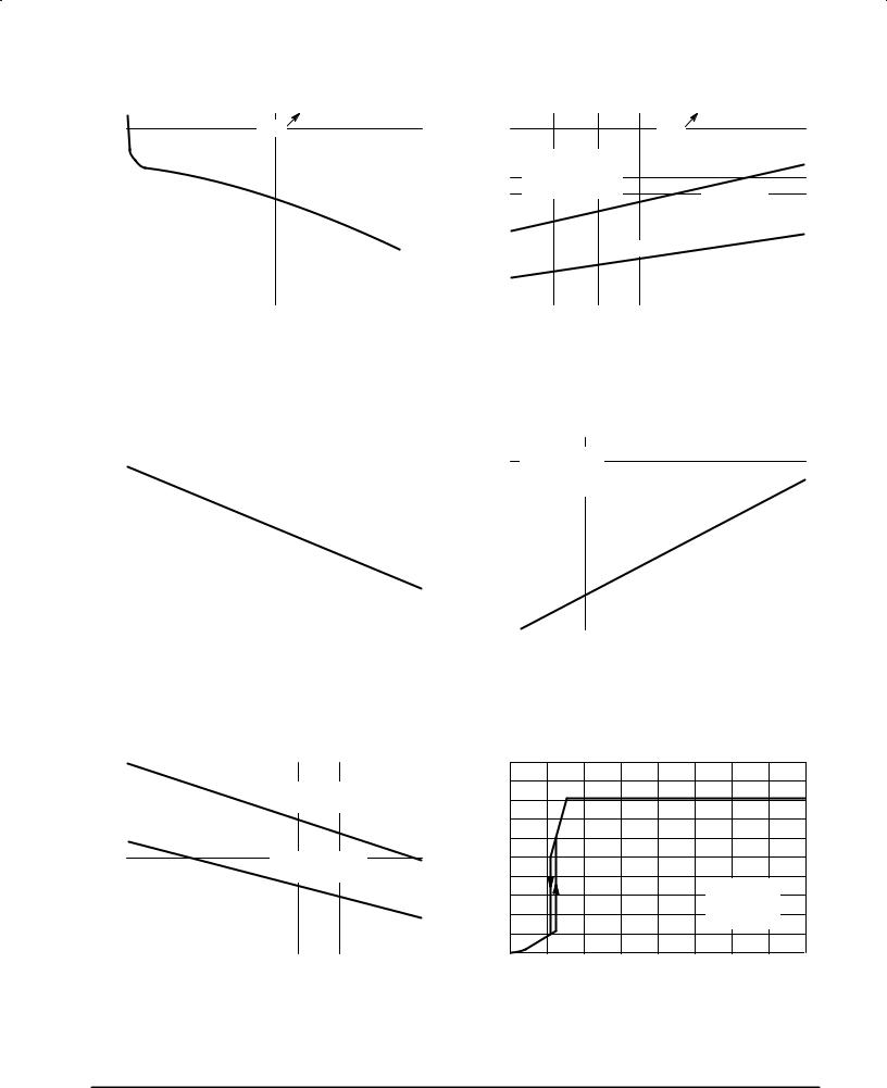
(V) |
|
|
Figure 1. Voltage Feedback Input Threshold |
|
|
|||||||
|
|
|
|
versus Temperature |
|
|
|
|||||
THRESHOLD |
5.17 |
|
|
|
|
|
|
|||||
|
|
|
|
|
|
|
|
|
|
|
||
|
5.25 |
|
|
|
|
|
|
|
|
|
|
|
INPUT |
|
VCC = |
12 V |
|
|
VFB(th) |
Max = 5.15 V |
|
|
|
||
5.09 |
|
|
|
|
|
|
||||||
|
|
|
|
|
|
|
|
|
|
|
||
|
|
|
|
|
|
|
|
|
|
|
||
FEEDBACK |
|
|
|
|
|
VFB(th) Typ = 5.05 V |
|
|
|
|||
5.01 |
|
|
|
|
|
|
|
|
|
|
|
|
VOLTAGE, |
|
|
|
|
|
VFB(th) Min = 4.95 V |
|
|
|
|||
4.93 |
|
|
|
|
|
|
|
|
||||
FB(th) |
|
|
|
|
|
|
|
|
||||
|
|
|
|
|
|
|
|
|
|
|
||
|
|
|
|
|
|
|
|
|
|
|
||
|
|
|
|
|
|
|
|
|
|
|
|
|
± 55 |
± 25 |
0 |
25 |
50 |
75 |
100 |
125 |
|||||
V |
4.85 |
|
|
|
TA, AMBIENT TEMPERATURE (°C) |
|
|
|
||||
|
|
|
|
|
|
|
||||||
|
|
|
|
|
|
|
|
|||||
Figure 3. Error Amp Open Loop Gain and
Phase versus Frequency
|
|
|
Figure 2. Voltage Feedback Input Bias |
|
|
||||||||||
|
|
|
|
|
Current versus Temperature |
|
|
|
|||||||
(nA) |
100 |
|
|
|
|
|
|
|
|
|
|
|
|
|
|
|
|
|
|
|
|
|
|
|
|
|
|
|
|
||
|
|
|
|
|
|
|
|
|
|
|
|
|
|
|
|
80 |
|
|
|
|
|
|
|
|
|
|
VCC = 12 V |
|
|
||
|
|
|
|
|
|
|
|
|
|
VFB = VFB(th) |
|
|
|||
CURRENTBIAS |
|
|
|
|
|
|
|
|
|
|
|
|
|
||
60 |
|
|
|
|
|
|
|
|
|
|
|
|
|
|
|
|
|
|
|
|
|
|
|
|
|
|
|
|
|
|
|
, INPUT |
40 |
|
|
|
|
|
|
|
|
|
|
|
|
|
|
|
|
|
|
|
|
|
|
|
|
|
|
|
|
||
|
|
|
|
|
|
|
|
|
|
|
|
|
|
||
20 |
|
|
|
|
|
|
|
|
|
|
|
|
|
|
|
|
|
|
|
|
|
|
|
|
|
|
|
|
|
||
IB |
|
|
|
|
|
|
|
|
|
|
|
|
|
|
|
|
|
|
|
|
|
|
|
|
|
|
|
|
|
|
|
I |
|
|
|
|
|
|
|
|
|
|
|
|
|
|
|
|
0 |
|
|
|
|
|
|
|
|
|
|
|
|
|
|
|
|
|
|
|
|
|
|
|
|
|
|
|
|
|
|
|
|
± 25 |
0 |
25 |
50 |
75 |
100 |
125 |
|||||||
|
± 55 |
||||||||||||||
TA, AMBIENT TEMPERATURE (°C)
Figure 4. Error Amp Output Saturation
versus Sink Current
GAINVOLTAGELOOPOPEN, (dB) |
100 |
|
|
|
VCC = 12 V |
0 |
|
VOLTAGESATURATIONOUTPUT(V) |
2.0 |
|
|
|
|
|
|
|
|
|
|
|
(DEGREES)PHASEEXCESS |
0.4 |
|
|
|
TA = +25°C |
|
||||
80 |
|
|
|
VComp = 3.25 V |
30 |
|
|
|
|
||||||
|
|
Gain |
|
RL = 100 k |
|
|
1.6 |
|
|
|
|
|
|||
|
|
|
|
|
|
|
|
|
|
|
|
||||
|
|
|
|
TA = +25°C |
|
|
|
|
|
|
|
|
|
||
|
60 |
|
|
|
60 |
|
|
|
|
|
|
|
|
||
|
|
|
|
|
|
|
|
1.2 |
|
|
|
|
|
||
|
|
|
|
|
|
|
|
|
|
|
|
|
|
|
|
|
40 |
|
|
|
|
Phase |
90 |
|
|
|
|
|
|
|
|
|
|
|
|
|
|
|
|
|
0.8 |
|
|
|
|
|
|
|
20 |
|
|
|
|
|
120 |
|
|
|
|
|
|
|
|
|
|
|
|
|
|
|
|
|
|
|
|
VCC = 12 V |
|
||
|
|
|
|
|
|
|
|
|
|
|
|
|
|
VFB = 5.5 V |
|
VOL |
0 |
|
|
|
|
|
150 |
φ, |
, |
|
|
|
|
|
|
|
|
|
|
|
|
|
sat |
|
|
|
|
|
|
||
A |
± 20 |
|
|
|
|
|
180 |
|
V |
0 |
|
|
|
|
|
|
100 |
1.0 k |
10 k |
100 k |
1.0 M |
|
|
0.4 |
0.8 |
1.2 |
1.6 |
2.0 |
|||
|
10 |
10 M |
|
|
0 |
||||||||||
|
|
|
f, FREQUENCY (Hz) |
|
|
|
|
|
|
ISink, OUTPUT SINK CURRENT (mA) |
|
||||
Figure 5. Oscillator Frequency Change |
Figure 6. Switch Output Duty Cycle |
f OSC, OSCILLATOR FREQUENCY CHANGE (%)
versus Temperature |
versus Compensation Voltage |
4.0
VCC = 12 V
0
± 4.0
± 8.0
± 12
± 55 ± 25 0 25 50 75 100 125
(%) |
100 |
|
|
|
|
|
|
|
|
|
|
|
|
|
|
CYCLE |
80 |
VCC = 12 V |
|
|
|
|
|
|
TA = +25°C |
|
|
|
|
|
|
DUTY |
60 |
|
|
|
|
|
|
OUTPUT |
40 |
|
|
|
|
|
|
|
|
|
|
|
|
|
|
DC, SWITCH |
20 |
|
|
|
|
|
|
0 |
|
|
|
|
|
|
|
|
2.0 |
2.5 |
3.0 |
3.5 |
4.0 |
4.5 |
|
|
1.5 |
TA, AMBIENT TEMPERATURE (°C) |
VComp, COMPENSATION VOLTAGE (V) |
MOTOROLA ANALOG IC DEVICE DATA |
3 |
|
MC34167 MC33167
Figure 7. Switch Output Source Saturation
(V) |
|
|
|
versus Source Current |
|
|
||||
SATURATION |
0 |
|
|
|
|
TA = +25°C |
|
|
||
|
|
|
|
VCC |
|
|
|
|
|
|
SOURCE |
± 0.5 |
|
|
|
|
|
|
|
|
|
|
|
|
|
|
|
|
|
|
||
±1.0 |
|
|
|
|
|
|
|
|
|
|
|
|
|
|
|
|
|
|
|
||
|
|
|
|
|
|
|
|
|
|
|
OUTPUT |
±1.5 |
|
|
|
|
|
|
|
|
|
|
|
|
|
|
|
|
|
|
||
|
|
|
|
|
|
|
|
|
||
± 2.0 |
|
|
|
|
|
|
|
|
|
|
|
|
|
|
|
|
|
|
|
||
SWITCH, |
|
|
|
|
|
|
|
|
|
|
± 2.5 |
|
|
|
|
|
|
|
|
|
|
|
|
|
|
|
|
|
|
|
||
|
|
|
|
|
|
|
|
|
|
|
sat± 3.0 |
|
|
|
|
|
|
|
|
|
|
|
|
|
|
|
|
|
|
|
||
|
2.0 |
4.0 |
6.0 |
|
8.0 |
|||||
V |
0 |
|
||||||||
ISource, SWITCH OUTPUT SOURCE CURRENT (A)
Figure 9. Switch Output Current Limit
Threshold versus Temperature
(A) |
7.2 |
|
|
|
|
|
|
|
|
|
|
|
|
|
|
|
|
|
|
|
|
|
|
|
|
|
|
|
|
|
|
||
THRESHOLDLIMIT |
|
|
|
|
|
|
|
|
|
|
VCC |
= 12 V |
|
|
|
|
|
|
|
|
|
|
|
|
|
|
|
Pins |
1, 2, 3 = |
Gnd |
|
|
|
|
6.8 |
|
|
|
|
|
|
|
|
|
|
|
|
|
|
|
|
|
|
|
|
|
|
|
|
|
|
|
|
|
|
|
|
, CURRENT |
6.4 |
|
|
|
|
|
|
|
|
|
|
|
|
|
|
|
|
|
|
|
|
|
|
|
|
|
|
|
|
|
|
||
|
|
|
|
|
|
|
|
|
|
|
|
|
|
|
||
6.0 |
|
|
|
|
|
|
|
|
|
|
|
|
|
|
|
|
|
|
|
|
|
|
|
|
|
|
|
|
|
|
|
||
|
|
|
|
|
|
|
|
|
|
|
|
|
|
|
||
pk(switch) |
5.6 |
|
|
|
|
|
|
|
|
|
|
|
|
|
|
|
|
|
|
|
|
|
|
|
|
|
|
|
|
|
|
||
I |
|
± 25 |
0 |
25 |
50 |
75 |
100 |
125 |
||||||||
|
± 55 |
|||||||||||||||
TA, AMBIENT TEMPERATURE (°C)
(V) |
|
|
|
Figure 11. Undervoltage Lockout |
|
|
|||||||||
6.0 |
|
|
Thresholds versus Temperature |
|
|
||||||||||
THRESHOLD |
|
|
|
|
|
|
|
VCC Increasing |
|
|
|
|
|||
|
6.5 |
|
|
|
|
|
|
|
|
|
|
|
|
|
|
|
|
|
|
|
|
|
|
|
Startup |
Threshold |
|
|
|
|
|
LOCKOUT |
5.5 |
|
|
|
|
|
|
|
|
|
|
|
|
|
|
|
|
|
|
|
|
|
|
|
|
|
|
|
|
||
UNDERVOLTAGE, |
|
|
|
|
|
|
|
Turn±Off Threshold |
|
|
|
|
|||
|
|
|
|
|
|
|
|
|
|
|
|
||||
5.0 |
|
|
|
|
|
|
|
VCC Decreasing |
|
|
|
|
|||
|
|
|
|
|
|
|
|
|
|
|
|
|
|
|
|
th(UVLO) |
4.5 |
|
|
|
|
|
|
|
|
|
|
|
|
|
|
|
|
|
|
|
|
|
|
|
|
|
|
|
|
||
|
|
|
|
|
|
|
|
|
|
|
|
|
|
||
4.0 |
|
|
|
|
|
|
|
|
|
|
|||||
|
|
|
TA, |
AMBIENT |
TEMPERATURE (°C) |
|
|
|
|
||||||
|
|
|
|
|
|
|
|
|
|
|
|
|
|
|
|
|
± 55 |
± 25 |
0 |
25 |
50 |
75 |
100 |
125 |
|||||||
V |
|
|
|
|
|
|
|
|
|
|
|
|
|
|
|
Figure 8. Negative Switch Output Voltage
versus Temperature
|
0 |
|
|
|
|
|
|
|
|
|
|
|
|
|
(V) |
|
|
|
|
|
Gnd |
|
|
|
|
|
|
|
|
± 0.2 |
|
|
|
|
|
|
|
|
|
|
|
|
||
|
|
|
|
|
|
|
|
|
|
|
|
|
||
VOLTAGE |
|
VCC = |
12 V |
|
|
|
|
|
|
|
|
|
|
|
|
|
|
|
|
|
|
|
|
|
|
|
|||
|
± 0.4 |
|
Pin 5 = 2.0 V |
|
|
|
|
|
|
|
|
|
|
|
|
|
Pins 1, 3 = Gnd |
|
|
|
|
|
|
|
|
|
|||
OUTPUT |
± 0.6 |
|
Pin 2 Driven Negative |
|
|
Isw |
= 100 |
μA |
|
|
|
|||
|
|
|
|
|
|
|
|
|
|
|||||
|
|
|
|
|
|
|
|
|
|
|
|
|
||
SWITCH, |
|
|
|
|
|
|
|
|
|
|
|
|
|
|
± 0.8 |
|
|
|
|
|
|
|
|
|
|
|
|
|
|
|
|
|
|
|
|
|
|
|
|
|
|
|
||
|
|
|
|
|
Isw = 10 mA |
|
|
|
|
|
|
|
||
|
|
|
|
|
|
|
|
|
|
|
|
|
||
sw |
±1.0 |
|
|
|
|
|
|
|
|
|
|
|
|
|
|
|
|
|
|
|
|
|
|
|
|
|
|
||
|
|
|
|
|
|
|
|
|
|
|
|
|
|
|
V |
±1.2 |
|
|
|
|
|
|
|
|
|
|
|
|
|
|
|
|
|
|
|
|
|
|
|
|
|
|
|
|
|
|
± 25 |
0 |
25 |
50 |
75 |
100 |
125 |
||||||
|
± 55 |
|||||||||||||
|
|
|
|
|
TA, AMBIENT TEMPERATURE (°C) |
|
|
|
|
|||||
Figure 10. Standby Supply Current
versus Supply Voltage
|
160 |
|
|
|
|
|
|
|
|
|
|
|
|
Pin 4 |
= VCC |
|
|
|
|
|
|
|
|
|
|
|
|
|
|
|
|
|
|
||
A) |
|
Pins 1, |
3, 5 = Gnd |
|
|
|
|
|
|
||
120 |
|
Pin 2 |
Open |
|
|
|
|
|
|
||
(μ |
|
|
|
|
|
|
|
||||
|
TA = |
+25°C |
|
|
|
|
|
|
|||
CURRENT |
80 |
|
|
|
|
|
|
|
|
|
|
|
|
|
|
|
|
|
|
|
|
||
|
|
|
|
|
|
|
|
|
|
||
,SUPPLY |
40 |
|
|
|
|
|
|
|
|
|
|
|
|
|
|
|
|
|
|
|
|
||
CC |
|
|
|
|
|
|
|
|
|
|
|
|
|
|
|
|
|
|
|
|
|
|
|
I |
|
|
|
|
|
|
|
|
|
|
|
|
0 |
|
|
|
|
|
|
|
|
|
|
|
|
|
|
|
|
|
|
|
|
|
|
|
10 |
20 |
30 |
40 |
|||||||
|
0 |
||||||||||
VCC, SUPPLY VOLTAGE (V)
Figure 12. Operating Supply Current
versus Supply Voltage
|
50 |
|
|
|
|
(mA) |
40 |
|
|
|
|
|
|
|
|
|
|
CURRENT |
30 |
|
|
|
|
|
|
|
|
|
|
SUPPLY |
20 |
|
|
Pin 4 = VCC |
|
|
|
|
|
||
|
|
|
Pins 1, 3 = Gnd |
|
|
, |
|
|
|
Pins 2, 5 Open |
|
CC |
10 |
|
|
|
|
|
|
TA = +25°C |
|
||
I |
|
|
|
|
|
|
0 |
10 |
20 |
30 |
40 |
|
0 |
VCC, SUPPLY VOLTAGE (V)
4 |
MOTOROLA ANALOG IC DEVICE DATA |
|
|
MC34167 MC33167 |
|
|
|
|
||
Figure 13. MC34167 Representative Block Diagram |
|
|
||||||
|
|
|
|
|
|
Vin |
|
|
+ |
|
|
Current |
|
4 |
|
|
|
|
|
Sense |
|
|
|
|||
|
|
|
|
Input Voltage/VCC |
|
|||
|
|
|
|
|
|
|
||
Oscillator |
|
|
|
|
Cin |
|
|
|
S |
|
|
|
|
|
|
||
CT |
|
|
|
|
Switch |
|
|
|
|
Q |
|
|
|
|
|
||
|
|
|
|
|
Output |
|
|
|
|
|
R |
|
|
|
2 |
|
|
Pulse Width |
|
|
|
Undervoltage |
|
|
||
|
PWM Latch |
|
|
|
|
|||
Modulator |
|
|
Lockout |
|
|
|
|
|
|
|
|
|
|
|
|
||
|
|
Thermal |
|
|
|
|
|
L |
|
|
Shutdown |
|
5.05 V |
|
|
|
|
|
|
|
|
|
|
|
|
|
|
|
|
+ |
Reference |
|
|
|
|
|
|
|
|
+ |
Voltage |
|
|
|
|
|
|
|
Error |
|
|
||
|
|
100 μA |
|
|
Feedback |
|
|
|
|
|
|
Amp |
|
|
|
||
|
|
|
|
|
Input |
|
|
|
|
|
|
|
|
|
|
|
|
|
|
|
|
|
|
1 |
R2 |
VO |
|
|
|
120 |
|
|
CO |
||
|
|
|
|
|
|
|||
Gnd |
3 |
Compensation |
5 |
CF |
RF |
|
|
|
= |
|
|
|
|
R1 |
Sink Only |
|||||
|
Positive True Logic |
|
|
||
|
|
|
|
||
Figure 14. Timing Diagram
4.1 V
Timing Capacitor CT
Compensation
2.3 V
ON
Switch Output
OFF
MOTOROLA ANALOG IC DEVICE DATA |
5 |
|
 Loading...