


MC34084P
Motorola MC34084P, MC34085BDW, MC34085BP, MC34080BP, MC34081BD Datasheet
...
$"%
HIGH PERFORMANCE
JFET INPUT
OPERATIONAL AMPLIFIERS
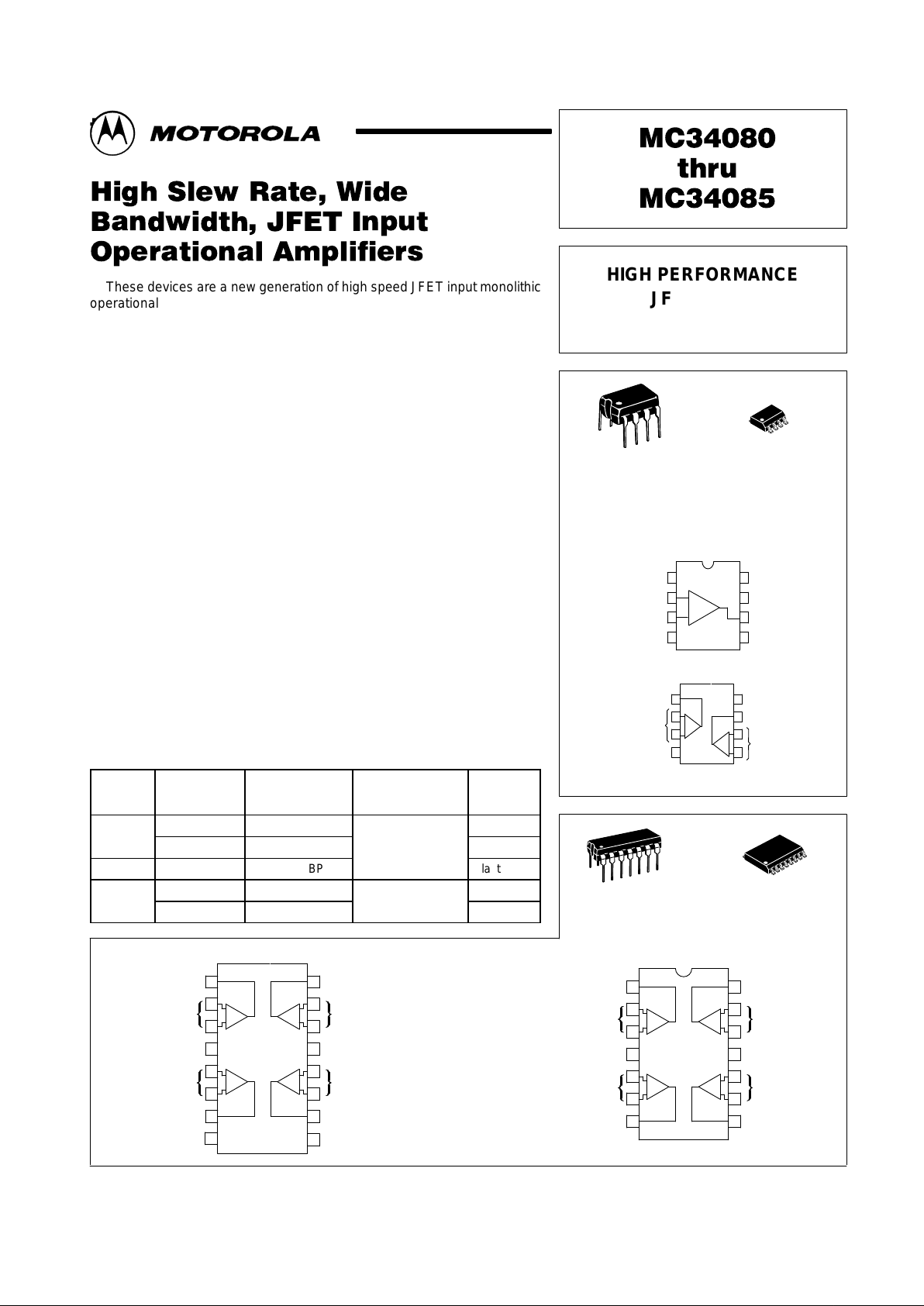
Order this document by MC34080/D
D SUFFIX
PLASTIC PACKAGE
CASE 751
(SO–8)
P SUFFIX
PLASTIC PACKAGE
CASE 626
DW SUFFIX
PLASTIC PACKAGE
CASE 751G
(SO–16L)
P SUFFIX
PLASTIC PACKAGE
CASE 646
PIN CONNECTIONS
PIN CONNECTIONS
(Single, Top View)
(Dual, Top View)
(Quad, Top View)
4
23
1
4
23
1
–
Offset Null
Noninv. Input
V
EE
Inv. Input
V
EE
Inputs 1
Output 1
NC
V
CC
Output
Offset Null
Inputs 2
Output 2
V
CC
1
2
3
4
8
7
6
5
+
1
2
3
4
8
7
6
5
–
+
–
+
Inputs 1
Output 1
V
CC
Inputs 2
Output 2
Inputs 1
Output 1
V
CC
Inputs 2
Output 2
NC
Output 4
Inputs 4
V
EE
Inputs 3
Output 3
Output 4
Inputs 4
V
EE
Inputs 3
Output 3
NC
1
2
3
4
5
6
710
11
12
13
14
15
16
8
9
1
2
3
4
5
6
78
9
10
11
12
13
14
–
+
–
+
+
–
+
–
–
+
–
+
+
–
+
–
1
8
1
8
14
1
16
1
1
MOTOROLA ANALOG IC DEVICE DATA
t
& $
&$ !%$
!"$ !"#
These devices are a new generation of high speed JFET input monolithic
operational amplifiers. Innovative design concepts along with JFET
technology provide wide gain bandwidth product and high slew rate.
Well–matched JFET input devices and advanced trim techniques ensure low
input offset errors and bias currents. The all NPN output stage features large
output voltage swing, no deadband crossover distortion, high capacitive
drive capability, excellent phase and gain margins, low open loop output
impedance, and symmetrical source/sink AC frequency response.
This series of devices is available in fully compensated or
decompensated (A
VCL
≤2) and is specified over a commercial temperature
range. They are pin compatible with existing Industry standard operational
amplifiers, and allow the designer to easily upgrade the performance of
existing designs.
• Wide Gain Bandwidth: 8.0 MHz for Fully Compensated Devices
Wide Gain Bandwidth: 16 MHz for Decompensated Devices
• High Slew Rate: 25 V/µs for Fully Compensated Devices
High Slew Rate: 50 V/µs for Decompensated Devices
• High Input Impedance: 10
12
Ω
• Input Offset Voltage: 0.5 mV Maximum (Single Amplifier)
• Large Output Voltage Swing: –14.7 V to +14 V for
Large Output Voltage Swing: VCC/VEE = ±15 V
• Low Open Loop Output Impedance: 30 Ω @ 1.0 MHz
• Low THD Distortion: 0.01%
• Excellent Phase/Gain Margins: 55°/7.6 dB for Fully Compensated
Devices
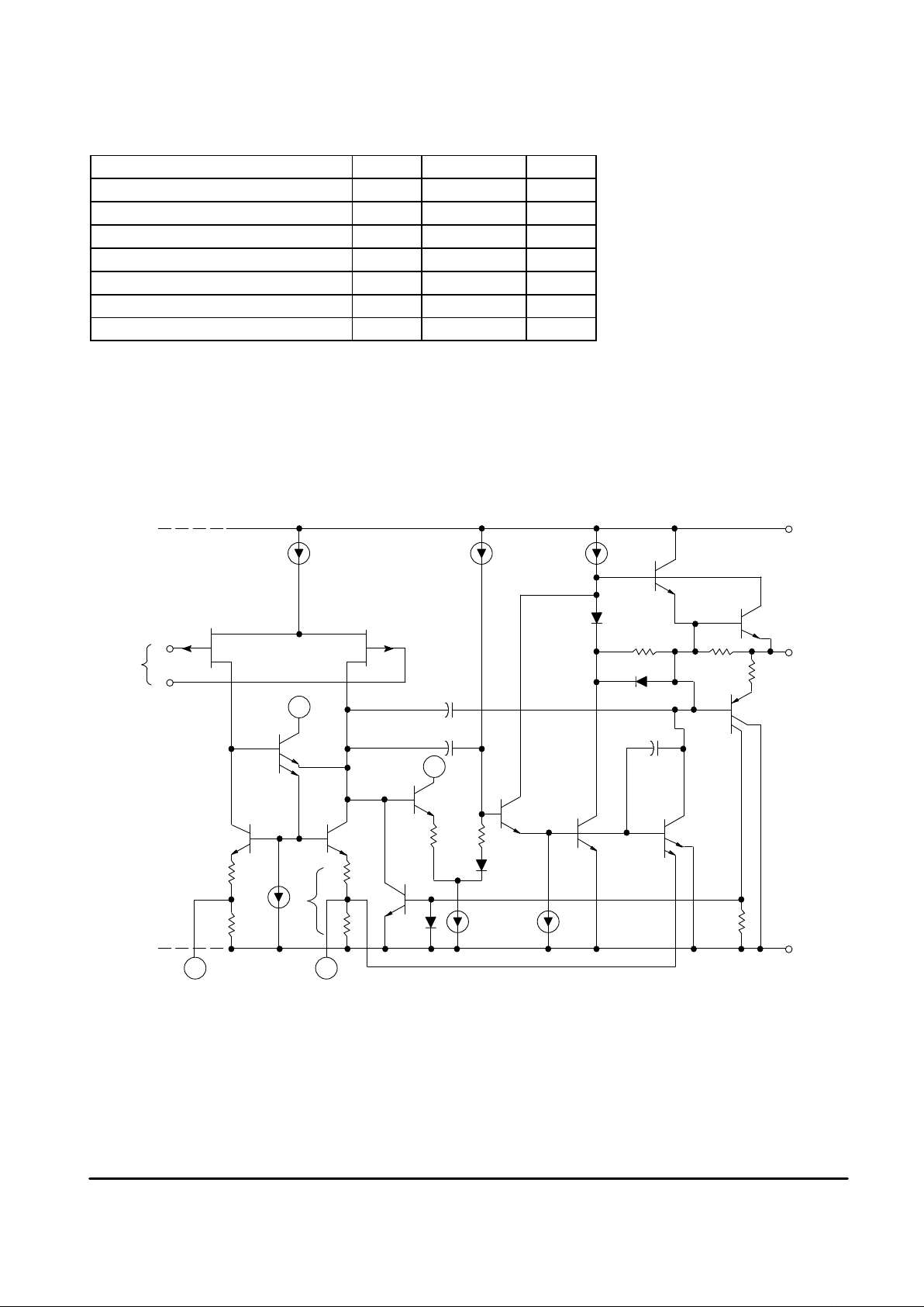
ORDERING INFORMATION
Op Amp
Function
Fully
Compen-
sated
A
VCL
≥2
Compensated
Operating
Temperature
Range
Package
MC34081BD MC34080BD
SO–8
Singl
e
MC34081BP MC34080BP
TA = 0° to +70°C
Plastic DIP
Dual MC34082P MC34083BP Plastic DIP
MC34084DW MC34085BDW
°
°
SO–16L
Quad
MC34084P MC34085BP
T
A
= 0° to +
70°C
Plastic DIP
Motorola, Inc. 1996 Rev 0
MC34080 thru MC34085
2
MOTOROLA ANALOG IC DEVICE DATA
MAXIMUM RATINGS
Rating Symbol Value Unit
Supply Voltage (from VCC to VEE) V
S
+44 V
Input Differential Voltage Range V
IDR
(Note 1) V
Input Voltage Range V
IR
(Note 1) V
Output Short Circuit Duration (Note 2) t
SC
Indefinite sec
Operating Ambient Temperature Range T
A
0 to +70 °C
Operating Junction Temperature T
J
+125 °C
Storage Temperature Range T
stg
– 65 to +165 °C
NOTES: 1. Either or both input voltages must not exceed the magnitude of VCC or VEE.
2.Power dissipation must be considered to ensure maximum junction temperature
(TJ) is not exceeded.
*Pins 1 & 5 (MC34080,081) should
not
be directly grounded or connected to VCC.
Inputs
–
+
J1 J2
Q1
V
CC
Q6
R1
240
18
D2
R
SC
Q7
C
M
Q4
Q3
Q2
Q8
Q9
500
Q10
R6
RM
Q11
D4
R3
1.0 k
Q5
C
C
C
F
20
pF
D3
V
EE
200
µ
A
Output
Null Adjust
(MC34080, 081)*
50 µA 850 µA
5.0
pF
3.0
pF
100
µ
A 300 µA
50 µA
500
Ω
R4
1.0 k
D1
R7
66 k
700
R2
+
+
1 5
Representative Schematic Diagram
(Each Amplifier)

MC34080 thru MC34085
3
MOTOROLA ANALOG IC DEVICE DATA
DC ELECTRICAL CHARACTERISTICS (V
CC
= +15 V , VEE = – 15 V, TA = T
low
to T
high
[Note 3], unless otherwise noted.)
Characteristics Symbol Min Typ Max Unit
Input Offset Voltage (Note 4)
Single
TA = +25°C
TA = 0° to +70°C (MC34080B, MC34081B)
Dual
TA = +25°C
TA = 0° to +70°C (MC34082, MC34083)
Quad
TA = +25°C
TA = 0° to +70°C (MC34084, MC34085)
V
IO
—
—
—
—
—
—
0.5
—
1.0
—
6.0
—
2.0
4.0
3.0
5.0
12
14
mV
Average Temperature Coefficient of Of fset Voltage ∆VIO/∆T — 10 — µV/°C
Input Bias Current (VCM = 0 Note 5)
TA = +25°C
TA = 0° to +70°C
I
IB
——0.06
—
0.2
4.0
nA
Input Offset Current (VCM = 0 Note 5)
TA = +25°C
TA = 0° to +70°C
I
IO
——0.02—0.1
2.0
nA
Large Signal Voltage Gain (VO = ±10 V, RL = 2.0 k)
TA = +25°C
TA = T
low
to T
high
A
VOL
25
15
80
—
—
—
V/mV
Output Voltage Swing
RL = 2.0 k, TA = +25°C
RL = 10 k, TA = +25°C
RL = 10 k, TA = T
low to Thigh
V
OH
13.2
13.4
13.4
13.7
13.9
—
—
—
—
V
RL = 2.0 k, TA = +25°C
RL = 10 k, TA = +25°C
RL = 10 k, TA = T
low to Thigh
V
OL
—
—
—
–14.1
–14.7
—
–13.5
–14.1
–14.0
Output Short Circuit Current (TA = +25°C)
Input Overdrive = 1.0 V , Output to Ground
Source
Sink
I
SC
20
20
31
28
—
—
mA
Input Common Mode Voltage Range
TA = +25°C
V
ICR
(VEE +4.0) to
(VCC – 2.0)
V
Common Mode Rejection Ratio (RS ≤ 10 k, TA = +25°C) CMRR 70 90 — dB
Power Supply Rejection Ratio (RS = 100 Ω, TA = 25°C) PSRR 70 86 — dB
Power Supply Current
Single
TA = +25°C
TA = T
low
to T
high
Dual
TA = +25°C
TA = T
low
to T
high
Quad
TA = +25°C
TA = T
low
to T
high
I
D
—
—
—
—
—
—
2.5
—
4.9
—
9.7
—
3.4
4.2
6.0
7.5
11
13
mA
NOTES: (continued)
3.T
low
=0°C for MC34080B T
high
= +70°C for MC34080B
0°C for MC34081B +70°C for MC34081B
0°C for MC34084 +70°C for MC34084
0°C for MC34085 +70°C for MC34085
4.See application information for typical changes in input offset voltage due to solderability and temperature cycling.
5.Limits at TA = +25°C are guaranteed by high temperature (T
high
) testing.
MC34080 thru MC34085
4
MOTOROLA ANALOG IC DEVICE DATA
AC ELECTRICAL CHARACTERISTICS
(VCC = +15 V , VEE = – 15 V, TA = +25°C, unless otherwise noted.)
Characteristics Symbol Min Typ Max Unit
Slew Rate (Vin = –10 V to +10 V, RL = 2.0 kΩ, CL = 100 pF)
Compensated AV = +1.0
AV = –1.0
Decompensated AV = +2.0
AV = –1.0
SR
20
—
35
—
25
30
50
50
—
—
—
—
V/µs
Settling Time (10 V Step, AV = –1.0)
To 0.10% (±1/2 LSB of 9–Bits)
To 0.01% (±1/2 LSB of 12–Bits)
t
s
——0.72
1.6
—
—
µs
Gain Bandwidth Product (f = 200 kHz)
Compensated
Decompensated
GBW
6.0128.0
16
—
—
MHz
Power Bandwidth (RL = 2.0 k, VO = 20 Vpp, THD = 5.0%)
Compensated AV = +1.0
Decompensated AV = – 1.0
BWp
——400
800——
kHz
Phase Margin (Compensated)
RL = 2.0 k
RL = 2.0 k, CL = 100 pF
φ
m
—
—
55
39
—
—
De-
grees
Gain Margin (Compensated)
RL = 2.0 k
RL = 2.0 k, CL = 100 pF
A
m
——7.6
4.5
—
—
dB
Equivalent Input Noise Voltage
RS = 100 Ω, f = 1.0 kHz
e
n
— 30 —
nV/ Hz√
Equivalent Input Noise Current (f = 1.0 kHz) I
n
— 0.01 —
pA/ Hz√
Input Capacitance C
i
— 5.0 — pF
Input Resistance r
i
— 10
12
— Ω
Total Harmonic Distortion
AV = +10, RL = 2.0 k, 2.0 ≤ VO ≤ 20 Vpp, f = 10 kHz
THD — 0.05 — %
Channel Separation (f = 10 kHz) — — 120 — dB
Open Loop Output Impedance (f = 1.0 MHz) Z
o
— 35 — Ω
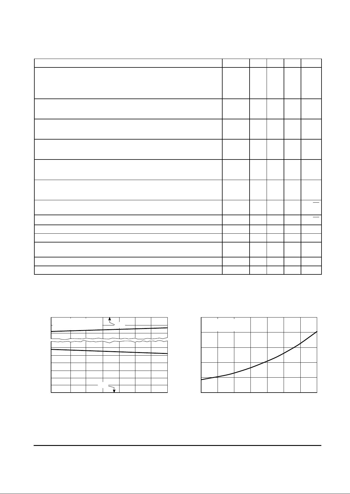
Figure 1. Input Common Mode Voltage Range
versus Temperature
Figure 2. Input Bias Current
versus Temperature
TA, AMBIENT TEMPERATURE (°C)
–55 –25 0 25 50 75 100 125
V , INPUT COMMON MODE VOLTAGE RANGE (V)
ICR
V
EE
VCC/VEE =
±
3.0 V to ±22 V
∆
VIO = 5.0 mA
V
CC
TA, AMBIENT TEMPERATURE (°C)
–55 –25 0 25 50 75 100 125
I , INPUT BIAS CURRENT (pA)
IB
VCC/VEE = ±15 V
VCM = 0 V
0
–1.0
3.0
2.0
1.0
0
100 k
10 k
1.0 k
100
10
1.0
MC34080 thru MC34085
5
MOTOROLA ANALOG IC DEVICE DATA
Sink
Source
VCC/VEE = ±15 V
RL
≤
0.1
Ω
∆
Vin = 1.0 V
VCC/VEE = +15 V
RL to V
CC
TA = 25°C
V
EE
V
CC
VCC/VEE = ±15 V
TA = 25
°
C
V
CC
V
EE
VCC/VEE = +15 V to +22 V
TA = 25
°
C
V
CC
V
EE
Sink
Source
V
O
, OUTPUT VOL TAGE SWING (V
pp
)
Figure 3. Input Bias Current versus
Input Common Mode Voltage
Figure 4. Output Voltage Swing
versus Supply Voltage
Figure 5. Output Saturation versus
Load Current
Figure 6. Output Saturation vesus
Load Resistance to Ground
Figure 7. Output Saturation versus
Load Resistance to V
CC
Figure 8. Output Short Circuit Current
versus Temperature
I
IB
–12 –8.0 –4.0 0 4.0 8.0 12
VIC, INPUT COMMON MODE VOLTAGE (V)
VCC/VEE =±15 V
TA = 25
°
C
0
±
5.0
±
10
±
15
±
20
±
25
VCC |VEE|, SUPPLY VOLT AGE (V)
RL = 10 k
RL Connected to Ground
TA = 25
°
C
RL = 2.0 k
0 4.0 8.0 12 16
IL, LOAD CURRENT (
±
mA)
V
sat
300 3.0 k 30 k 300 k
RL, LOAD RESISTANCE T O GROUND (
Ω
)
300 3.0 k 30 k 300 k
RL, LOAD RESISTANCE T O VCC (
Ω
)
–55 –25 0 25 50 75 100 125
I , OUTPUT SHORT CIRCUIT CURRENT (mA)
SC
TA, AMBIENT TEMPERATURE (°C)
, INPUT BIAS CURRENT (pA), OUTPUT SA TURATION VOLTAGE (V)
V
sat
, OUTPUT SA TURATION VOLTAGE (V)
V
sat
, OUTPUT SA TURATION VOLTAGE (V)
140
120
100
80
60
40
20
50
40
30
20
10
0
0
–1.0
–2.0
–3.0
1.0
0
0
–2.0
–4.0
2.0
1.0
0
0
–0.4
–0.8
2.0
1.0
0
40
30
10
0
20
 Loading...