


MOTOROLA MC34084DWR2, MC34080BD, MC34080BDR2, MC34084DW, MC34083BP Datasheet
...Order this document by MC34080/D
t |
|
|
MC34080 |
|
|
|
|
|
|
|
thru |
High Slew |
Rate, |
Wide |
MC34085 |
|
|
|
|
Bandwidth, |
JFET |
Input |
|
Operational |
Amplifiers |
|
|
|
These devices are a new generation of high speed JFET input monolithic |
HIGH PERFORMANCE |
||||||||||||||||||||||||
|
|
|
JFET INPUT |
|
||||||||||||||||||||||
operational amplifiers. Innovative design concepts along with JFET |
|
|
|
|||||||||||||||||||||||
technology provide wide gain bandwidth product and high slew rate. |
OPERATIONAL AMPLIFIERS |
|||||||||||||||||||||||||
Well±matched JFET input devices and advanced trim techniques ensure low |
|
|
|
|
|
|
|
|
|
|
|
|||||||||||||||
input offset errors and bias currents. The all NPN output stage features large |
|
|
|
|
|
|
|
|
|
|
|
|||||||||||||||
output voltage swing, no deadband crossover distortion, high capacitive |
|
|
|
|
|
|
|
|
|
|
|
|||||||||||||||
drive capability, excellent phase and gain margins, low open loop output |
|
|
|
|
|
|
|
|
|
|
|
|||||||||||||||
impedance, and symmetrical source/sink AC frequency response. |
|
|
|
|
|
|
|
|
|
|
|
|||||||||||||||
|
This series of |
devices |
is |
|
|
available in |
fully compensated or |
|
|
|
|
|
|
|
|
|
|
|
||||||||
decompensated (AVCL≤2) and is specified over a commercial temperature |
8 |
|
|
|
|
|
|
|
8 |
1 |
||||||||||||||||
|
|
|
|
|
|
|
|
|
||||||||||||||||||
range. They are pin compatible with existing Industry standard operational |
1 |
|
|
|
|
|
|
|
|
|
|
|||||||||||||||
amplifiers, and allow the designer to easily upgrade the performance of |
P SUFFIX |
|
|
|
|
|
D SUFFIX |
|||||||||||||||||||
existing designs. |
|
|
|
|
|
|
|
|
|
|
|
|
|
PLASTIC PACKAGE |
|
PLASTIC PACKAGE |
||||||||||
• Wide Gain Bandwidth: 8.0 MHz for Fully Compensated Devices |
CASE 626 |
|
|
|
|
|
CASE 751 |
|||||||||||||||||||
|
|
|
|
|
|
|
|
|
(SO±8) |
|||||||||||||||||
|
|
|
|
|
16 MHz for Decompensated Devices |
|
|
|
|
|
|
|
|
|
|
|||||||||||
|
|
|
|
|
|
|
|
PIN CONNECTIONS |
||||||||||||||||||
• High Slew Rate: 25 V/μs for Fully Compensated Devices |
|
|
|
|||||||||||||||||||||||
|
|
|
50 V/μs for Decompensated Devices |
|
|
|
|
|
|
|
|
|
|
|
|
|||||||||||
• High Input Impedance: 1012Ω |
|
|
|
|
|
|
|
|
|
Offset Null |
1 |
|
|
|
|
8 |
NC |
|||||||||
• Input Offset Voltage: 0.5 mV Maximum (Single Amplifier) |
|
Inv. Input |
2 |
± |
|
|
|
7 |
VCC |
|||||||||||||||||
|
|
|
|
|
|
|||||||||||||||||||||
• Large Output Voltage Swing: ±14.7 V to +14 V for |
|
Noninv. Input |
3 |
+ |
|
|
|
6 |
Output |
|||||||||||||||||
|
|
|
|
|
|
V |
CC |
/V |
EE |
= ±15 V |
|
|
|
V |
4 |
|
|
|
|
5 |
Offset Null |
|||||
|
|
|
|
|
|
|
|
|
|
|
|
|
|
EE |
|
|
|
|
|
|
|
|
||||
• Low Open Loop Output Impedance: 30 Ω @ 1.0 MHz |
|
|
|
|
(Single, Top View) |
|
||||||||||||||||||||
• Low THD Distortion: 0.01% |
|
|
|
|
|
|
|
|
|
|
|
|
|
|
||||||||||||
|
|
|
|
|
|
|
|
|
|
|
|
|
|
|
|
|
|
|
|
|
||||||
• |
|
|
|
|
|
|
|
|
|
° |
|
|
|
|
|
Output 1 |
1 |
|
|
|
8 |
|
V |
CC |
||
|
Excellent Phase/Gain Margins: 55 /7.6 dB for Fully Compensated |
|
|
|
|
|
|
|
|
|
|
|||||||||||||||
|
Devices |
|
|
|
|
|
|
|
|
|
|
|
|
|
|
|
Inputs 1 |
2 |
± |
|
|
7 |
|
Output 2 |
||
|
|
|
|
|
|
|
|
|
|
|
|
|
|
|
|
|
3 |
+ |
|
|
6 |
|
|
|
||
|
|
|
|
|
|
|
|
|
|
|
|
|
|
|
|
|
|
|
|
± |
|
Inputs 2 |
||||
|
|
|
|
|
|
|
|
|
|
|
|
|
|
|
|
|
|
|
|
|
|
|
|
|||
|
|
|
|
|
|
|
|
|
|
|
|
|
|
|
|
|
|
VEE |
4 |
|
|
+ |
5 |
|
||
|
|
|
|
ORDERING INFORMATION |
|
|
|
|
|
|
|
|
||||||||||||||
|
|
|
|
|
|
|
|
|
|
|
|
|
||||||||||||||
Op Amp |
Fully |
|
|
AVCL≥ |
|
2 |
|
|
Operating |
|
|
|
|
(Dual, Top View) |
|
|
||||||||||
Compen- |
|
|
|
|
Temperature |
Package |
|
|
|
|
|
|
|
|
|
|
|
|||||||||
Function |
sated |
|
Compensated |
|
Range |
|
|
|
|
|
|
|
|
|
|
|
||||||||||
|
Single |
MC34081BD |
MC34080BD |
|
|
|
SO±8 |
|
|
|
|
|
|
|
|
|
|
|
||||||||
|
MC34081BP |
MC34080BP |
|
TA = 0° to +70°C |
Plastic DIP |
|
|
|
|
|
|
|
|
|
|
|
||||||||||
|
|
|
|
|
|
|
|
|
|
|
|
|
|
|||||||||||||
|
Dual |
MC34082P |
|
MC34083BP |
|
|
|
Plastic DIP |
14 |
|
|
|
|
|
|
16 |
|
|
|
|||||||
|
|
|
|
|
|
|
|
|
|
|
|
|
|
|
||||||||||||
|
|
MC34084DW |
MC34085BDW |
|
|
SO±16L |
1 |
|
|
|
|
|
|
|
|
|
1 |
|||||||||
|
Quad |
TA |
= 0° to +70°C |
|
|
|
|
|
|
|
|
|
|
|||||||||||||
|
MC34084P |
|
MC34085BP |
|
Plastic DIP |
P SUFFIX |
|
|
|
|
|
|
DW SUFFIX |
|||||||||||||
|
|
|
|
|
|
|
|
|
|
|
|
|
|
|
|
PLASTIC PACKAGE |
|
|
PLASTIC PACKAGE |
|||||||
|
|
|
|
|
|
|
|
|
|
|
|
|
|
|
|
CASE 646 |
|
|
|
|
|
|
CASE 751G |
|||
|
|
|
|
|
|
|
|
|
|
|
|
|
|
PIN CONNECTIONS |
|
|
|
|
|
|
|
|
|
(SO±16L) |
||
|
|
Output 1 |
1 |
|
|
|
|
|
16 Output 4 |
|
|
Output 1 |
1 |
|
|
|
|
|
14 |
Output 4 |
||||||
|
|
Inputs 1 |
2 |
± |
|
|
± |
15 |
|
|
|
|
|
2 |
|
|
|
|
|
13 |
|
|
|
|||
|
|
|
|
|
|
|
|
Inputs 4 |
|
|
Inputs 1 |
± |
|
|
± |
|
|
|
Inputs 4 |
|||||||
|
|
|
|
|
|
|
|
|
|
|
|
|
|
|
|
|
||||||||||
|
|
|
3 |
+ |
1 |
4 |
+ |
14 |
|
|
|
|
|
+ |
|
|
|
|
||||||||
|
|
|
|
|
|
|
|
|
|
|
3 |
+ |
1 |
4 |
|
12 |
|
|
|
|||||||
|
|
|
|
|
|
|
|
|
|
|
|
|
|
|
|
|
|
|
|
|
|
|
||||
|
|
V |
4 |
|
|
|
|
|
13 V |
|
|
|
V |
4 |
|
|
|
|
|
11 |
V |
|
||||
|
|
CC |
|
|
|
|
|
|
|
|
|
EE |
|
|
|
|
|
|
|
|
|
|||||
|
|
|
|
|
|
|
|
|
|
|
|
|
|
|
|
CC |
|
|
|
|
|
|
|
|
EE |
|
|
|
Inputs 2 |
5 |
+ |
|
|
+ |
12 |
|
|
|
|
|
5 |
|
|
|
+ |
|
10 |
|
|
|
|||
|
|
|
|
|
|
|
|
Inputs 3 |
|
|
Inputs 2 |
+ |
|
|
|
|
|
|
||||||||
|
|
|
± |
2 |
3 |
± |
|
|
|
|
|
|
|
|
|
|
|
|
Inputs 3 |
|||||||
|
|
|
6 |
11 |
|
|
6 |
± 2 |
3 |
± |
|
9 |
|
|
||||||||||||
|
|
|
|
|
|
|
|
|
|
|
|
|
|
|
|
|
||||||||||
|
|
|
|
|
|
|
|
|
|
|
|
|
|
|
|
|
|
|
|
|
|
|
|
|
||
|
|
Output 2 |
7 |
|
|
|
|
|
10 Output 3 |
|
|
Output 2 |
7 |
|
|
|
|
|
8 |
Output 3 |
||||||
|
|
|
|
|
|
|
|
|
|
|
|
|
|
|
|
|
|
|
|
|
||||||
|
|
NC 8 |
|
|
|
|
|
|
9 NC |
|
|
|
|
|
(Quad, Top View) |
|
|
|
|
|
||||||
|
|
|
|
|
|
|
|
|
|
|
|
|
|
|
|
|
|
|
|
|
|
|
||||
|
|
|
|
|
|
|
|
|
|
|
|
|
|
|
|
Motorola, Inc. 1996 |
|
|
|
|
|
|
|
Rev 0 |
||
MC34080 thru MC34085
MAXIMUM RATINGS
Rating |
Symbol |
Value |
Unit |
|
|
|
|
Supply Voltage (from VCC to VEE) |
VS |
+44 |
V |
Input Differential Voltage Range |
VIDR |
(Note 1) |
V |
Input Voltage Range |
VIR |
(Note 1) |
V |
Output Short Circuit Duration (Note 2) |
tSC |
Indefinite |
sec |
Operating Ambient Temperature Range |
TA |
0 to +70 |
°C |
Operating Junction Temperature |
TJ |
+125 |
°C |
Storage Temperature Range |
Tstg |
± 65 to +165 |
°C |
NOTES: 1. Either or both input voltages must not exceed the magnitude of VCC or VEE.
2.Power dissipation must be considered to ensure maximum junction temperature (TJ) is not exceeded.
|
|
|
|
|
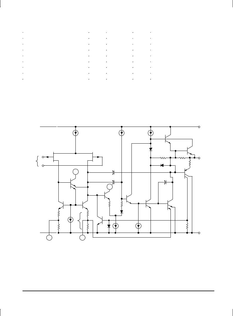
Representative Schematic Diagram |
|
|
|
|||||
|
|
|
|
|
|
(Each Amplifier) |
|
|
|
|
|
||
|
|
|
|
|
|
|
|
|
|
|
|
|
VCC |
|
|
|
|
200 μA |
|
|
50 μA |
|
|
850 μA |
|
|
|
|
|
|
|
|
|
|
|
|
|
|
|
Q1 |
|
|
|
|
|
|
|
|
|
|
D1 |
R1 |
|
Q6 |
|
|
|
|
|
|
|
|
|
|
|
|
|
||
± |
|
J1 |
|
|
J2 |
|
|
|
|
|
240 |
18 |
Output |
|
|
|
|
|
|
|
|
|
|
||||
Inputs |
|
|
|
|
|
|
|
|
|
|
|
RSC |
|
|
|
|
|
|
|
|
|
|
|
|
700 |
||
+ |
|
|
|
|
|
|
5.0 |
|
|
|
D2 |
|
R2 |
|
|
|
|
|
|
CC |
|
|
|
|
|
||
|
|
|
+ |
|
|
pF |
|
|
|
|
|
||
|
|
|
|
|
|
|
|
|
|
Q7 |
|||
|
|
|
|
|
|
|
|
|
|
|
|
|
|
|
|
|
|
|
|
CF |
20 |
|
|
|
CM |
|
|
|
|
|
|
|
|
pF |
|
|
|
|
|
||
|
|
|
Q8 |
|
|
|
|
|
|
|
|
||
|
|
|
|
|
|
|
|
|
|
|
|
|
|
|
|
|
|
|
|
+ |
|
|
|
|
3.0 |
|
|
|
|
|
|
|
|
|
|
|
|
|
pF |
|
|
|
|
|
|
|
|
Q5 |
|
|
|
|
|
|
|
|
|
|
|
|
|
|
|
Q2 |
|
|
Q3 |
|
|
|
|
|
|
|
Q10 |
R3 |
R4 |
|
|
|
Q4 |
|
|
|
|
Q9 |
|
|
|
|
|
|
|
||||
|
|
|
|
1.0 k |
1.0 k |
|
|
|
|
|
|
||
|
|
|
|
|
|
|
|
|
|
|
|
||
|
|
500 |
|
|
R6 |
|
|
D3 |
|
|
|
|
|
|
|
|
|
|
|
|
|
|
|
|
|
||
|
|
50 μA |
500 |
|
|
Q11 |
|
|
|
|
|
|
|
|
|
|
Ω |
|
|
|
|
|
|
|
|
|
|
|
|
|
|
|
|
D4 |
100 |
μ |
300 |
μ |
A |
R7 |
|
|
|
|
|
|
|
A |
|
66 k |
|
||||
|
|
|
|
|
|
|
|
|
|
|
|
|
|
|
|
|
|
|
RM |
|
|
|
|
|
|
|
VEE |
|
1 |
Null Adjust |
5 |
|
|
|
|
|
|
|
|
||
|
|
|
|
|
|
|
|
|
|
||||
|
|
|
|
|
|
|
|
|
|
|
|
||
|
|
(MC34080, 081)* |
|
|
|
|
|
|
|
|
|
|
|
*Pins 1 & 5 (MC34080,081) should not be directly grounded or connected to VCC.
2 |
MOTOROLA ANALOG IC DEVICE DATA |

MC34080 thru MC34085
DC ELECTRICAL CHARACTERISTICS (VCC = +15 V, VEE = ± 15 V, TA = Tlow to Thigh [Note 3], unless otherwise noted.)
Characteristics |
|
|
Symbol |
Min |
|
Typ |
Max |
Unit |
|
|
|
|
|
|
|
|
|
Input Offset Voltage (Note 4) |
|
|
VIO |
|
|
|
|
mV |
Single |
|
|
|
|
|
|
|
|
TA = +25°C |
|
|
|
Ð |
|
0.5 |
2.0 |
|
TA = 0° to +70°C (MC34080B, MC34081B) |
|
|
|
Ð |
|
Ð |
4.0 |
|
Dual |
|
|
|
|
|
|
|
|
TA = +25°C |
|
|
|
Ð |
|
1.0 |
3.0 |
|
TA = 0° to +70°C (MC34082, MC34083) |
|
|
|
Ð |
|
Ð |
5.0 |
|
Quad |
|
|
|
|
|
|
|
|
TA = +25°C |
|
|
|
Ð |
|
6.0 |
12 |
|
TA = 0° to +70°C (MC34084, MC34085) |
|
|
|
Ð |
|
Ð |
14 |
|
Average Temperature Coefficient of Offset Voltage |
|
|
VIO/ T |
Ð |
|
10 |
Ð |
μV/°C |
Input Bias Current (VCM = 0 Note 5) |
|
|
IIB |
|
|
|
|
|
TA = +25°C |
|
|
|
Ð |
|
0.06 |
0.2 |
nA |
TA = 0° to +70°C |
|
|
|
Ð |
|
Ð |
4.0 |
|
Input Offset Current (VCM = 0 Note 5) |
|
|
IIO |
|
|
|
|
|
TA = +25°C |
|
|
|
Ð |
|
0.02 |
0.1 |
nA |
TA = 0° to +70°C |
|
|
|
Ð |
|
Ð |
2.0 |
|
Large Signal Voltage Gain (VO = ±10 V, RL = 2.0 k) |
|
|
AVOL |
|
|
|
|
V/mV |
TA = +25°C |
|
|
|
25 |
|
80 |
Ð |
|
TA = Tlow to Thigh |
|
|
|
15 |
|
Ð |
Ð |
|
Output Voltage Swing |
|
|
VOH |
|
|
|
|
V |
RL = 2.0 k, TA = +25°C |
|
|
|
13.2 |
|
13.7 |
Ð |
|
RL = 10 k, TA = +25°C |
|
|
|
13.4 |
|
13.9 |
Ð |
|
RL = 10 k, TA = Tlow to Thigh |
|
|
|
13.4 |
|
Ð |
Ð |
|
RL = 2.0 k, TA = +25°C |
|
|
VOL |
Ð |
|
±14.1 |
±13.5 |
|
RL = 10 k, TA = +25°C |
|
|
|
Ð |
|
±14.7 |
±14.1 |
|
RL = 10 k, TA = Tlow to Thigh |
|
|
|
Ð |
|
Ð |
±14.0 |
|
Output Short Circuit Current (TA = +25°C) |
|
|
ISC |
|
|
|
|
mA |
Input Overdrive = 1.0 V, Output to Ground |
|
|
|
|
|
|
|
|
Source |
|
|
|
20 |
|
31 |
Ð |
|
Sink |
|
|
|
20 |
|
28 |
Ð |
|
|
|
|
|
|
|
|
|
|
Input Common Mode Voltage Range |
|
|
VICR |
(VEE +4.0) to |
V |
|||
TA = +25°C |
|
|
|
|
(VCC ± 2.0) |
|
||
Common Mode Rejection Ratio (RS ≤ 10 k, TA = +25°C) |
|
CMRR |
70 |
|
90 |
Ð |
dB |
|
Power Supply Rejection Ratio (RS = 100 Ω, TA = 25°C) |
|
PSRR |
70 |
|
86 |
Ð |
dB |
|
Power Supply Current |
|
|
ID |
|
|
|
|
mA |
Single |
|
|
|
|
|
|
|
|
TA = +25°C |
|
|
|
Ð |
|
2.5 |
3.4 |
|
TA = Tlow to Thigh |
|
|
|
Ð |
|
Ð |
4.2 |
|
Dual |
|
|
|
|
|
|
|
|
TA = +25°C |
|
|
|
Ð |
|
4.9 |
6.0 |
|
TA = Tlow to Thigh |
|
|
|
Ð |
|
Ð |
7.5 |
|
Quad |
|
|
|
|
|
|
|
|
TA = +25°C |
|
|
|
Ð |
|
9.7 |
11 |
|
TA = Tlow to Thigh |
|
|
|
Ð |
|
Ð |
13 |
|
NOTES: (continued) |
|
|
|
|
|
|
|
|
3. Tlow = 0°C for MC34080B |
Thigh = |
+70°C for MC34080B |
|
|
|
|
|
|
MC34081B |
|
MC34081B |
|
|
|
|
|
|
MC34084 |
|
MC34084 |
|
|
|
|
|
|
MC34085 |
|
MC34085 |
|
|
|
|
|
|
4.See application information for typical changes in input offset voltage due to solderability and temperature cycling.
5.Limits at TA = +25°C are guaranteed by high temperature (Thigh) testing.
MOTOROLA ANALOG IC DEVICE DATA |
3 |
|
MC34080 thru MC34085
AC ELECTRICAL CHARACTERISTICS (VCC = +15 V, VEE = ± 15 V, TA = +25°C, unless otherwise noted.)
|
Characteristics |
Symbol |
Min |
Typ |
Max |
Unit |
|||
|
|
|
|
|
|
|
|
||
Slew Rate (Vin = ±10 V to +10 V, RL = 2.0 kΩ, CL = 100 pF) |
SR |
|
|
|
V/μs |
||||
Compensated |
AV = +1.0 |
|
20 |
25 |
Ð |
|
|
|
|
|
AV = ±1.0 |
|
Ð |
30 |
Ð |
|
|
|
|
Decompensated |
AV = +2.0 |
|
35 |
50 |
Ð |
|
|
|
|
|
AV = ±1.0 |
|
Ð |
50 |
Ð |
|
|
|
|
Settling Time (10 V Step, AV = ±1.0) |
ts |
|
|
|
μs |
|
|
||
To 0.10% (±1/ LSB of 9±Bits) |
|
Ð |
0.72 |
Ð |
|
|
|
|
|
2 |
|
|
|
|
|
|
|
|
|
To 0.01% (±1/ LSB of 12±Bits) |
|
Ð |
1.6 |
Ð |
|
|
|
|
|
2 |
|
|
|
|
|
|
|
|
|
Gain Bandwidth Product (f = 200 kHz) |
GBW |
|
|
|
MHz |
||||
Compensated |
|
|
6.0 |
8.0 |
Ð |
|
|
|
|
Decompensated |
|
|
12 |
16 |
Ð |
|
|
|
|
|
|
|
|
|
|
|
|
||
Power Bandwidth (RL = 2.0 k, VO = 20 Vpp, THD = 5.0%) |
BWp |
|
|
|
kHz |
||||
Compensated AV = +1.0 |
|
Ð |
400 |
Ð |
|
|
|
|
|
Decompensated AV = ± 1.0 |
|
Ð |
800 |
Ð |
|
|
|
|
|
Phase Margin (Compensated) |
φm |
|
|
|
De- |
||||
RL = 2.0 k |
|
|
Ð |
55 |
Ð |
grees |
|||
RL = 2.0 k, CL = 100 pF |
|
Ð |
39 |
Ð |
|
|
|
|
|
Gain Margin (Compensated) |
Am |
|
|
|
dB |
|
|
||
RL = 2.0 k |
|
|
Ð |
7.6 |
Ð |
|
|
|
|
RL = 2.0 k, CL = 100 pF |
|
Ð |
4.5 |
Ð |
|
|
|
|
|
Equivalent Input Noise Voltage |
en |
Ð |
30 |
Ð |
nV/√ |
|
|
||
|
Hz |
|
|||||||
RS = 100 Ω, f = 1.0 kHz |
|
|
|
|
|
|
|
|
|
Equivalent Input Noise Current (f = 1.0 kHz) |
In |
Ð |
0.01 |
Ð |
pA/ √ |
|
|
||
|
Hz |
|
|||||||
Input Capacitance |
|
Ci |
Ð |
5.0 |
Ð |
pF |
|
|
|
Input Resistance |
|
ri |
Ð |
1012 |
Ð |
Ω |
|
|
|
Total Harmonic Distortion |
THD |
Ð |
0.05 |
Ð |
% |
|
|
|
|
AV = +10, RL = 2.0 k, 2.0 ≤ VO ≤ 20 Vpp, f = 10 kHz |
|
|
|
|
|
|
|
|
|
Channel Separation (f = 10 kHz) |
Ð |
Ð |
120 |
Ð |
dB |
|
|
||
|
|
|
|
|
|
|
|
||
Open Loop Output Impedance (f = 1.0 MHz) |
Zo |
Ð |
35 |
Ð |
Ω |
|
|
||
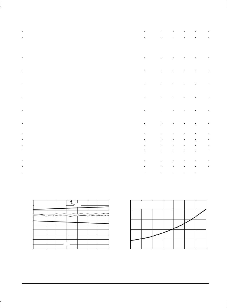
VICR , INPUT COMMON MODE VOLTAGE RANGE (V)
Figure 1. Input Common Mode Voltage Range
versus Temperature
0 |
|
VCC/VEE = ±3.0 V to ±22 V |
VCC |
VIO = 5.0 mA |
±1.0
3.0
2.0
1.0
VEE 0
0 
±55 |
±25 |
0 |
25 |
50 |
75 |
100 |
125 |
|
|
TA, AMBIENT TEMPERATURE (°C) |
|
|
|||
Figure 2. Input Bias Current
versus Temperature
|
100 k |
VCC/VEE = ±15 V |
|
|
|
|
|
|
|
|
|
|
|
|
|
||
(pA) |
10 k |
VCM = 0 V |
|
|
|
|
|
|
|
|
|
|
|
|
|
||
|
|
|
|
|
|
|
|
|
CURRENT |
1.0 k |
|
|
|
|
|
|
|
|
|
|
|
|
|
|
|
|
, INPUT BIAS |
100 |
|
|
|
|
|
|
|
10 |
|
|
|
|
|
|
|
|
IB |
|
|
|
|
|
|
|
|
I |
|
|
|
|
|
|
|
|
|
1.0 |
±25 |
0 |
25 |
50 |
75 |
100 |
125 |
|
±55 |
|||||||
|
|
|
TA, AMBIENT TEMPERATURE (°C) |
|
|
|||
4 |
MOTOROLA ANALOG IC DEVICE DATA |

MC34080 thru MC34085
I IB , INPUT BIAS CURRENT (pA)
Figure 3. Input Bias Current versus
Input Common Mode Voltage
140
120VCC/VEE = ±15 V TA = 25°C
100
80
60
40
20 ±12 ±8.0 ±4.0 0 4.0 8.0 12
VIC, INPUT COMMON MODE VOLTAGE (V)
VO, OUTPUT VOLTAGE SWING (Vpp)
Figure 4. Output Voltage Swing
versus Supply Voltage
50 |
|
|
|
|
|
|
|
|
|
|
|
|
|
|
|
|
|
|
|
|
|
|
|
|
|
|
|
|
|
|
|
|
|
|
|
|
|
|
40 |
|
RL |
Connected |
to |
Ground |
|
|
|
|
|
|
|
|
|
TA = |
25°C |
|
|
|
|
|
|
|
|
|
30 |
|
|
|
|
|
|
|
|
|
|
|
|
|
|
|
|
RL = 10 k |
|
|
R |
L = 2.0 |
k |
|
|
|
|
|
|
|
|
|
|
|
|
||||
20 |
|
|
|
|
|
|
|
|
|
|
|
|
|
|
|
|
|
|
|
|
|
|
|
|
|
10 |
|
|
|
|
|
|
|
|
|
|
|
|
|
|
|
|
|
|
|
|
|
|
|
|
|
|
|
|
|
|
|
|
|
|
|
|
|
|
0 |
|
|
|
|
|
|
|
|
|
|
|
|
|
|
|
|
|
|
|
|
|
|
|
|
|
0 |
±5.0 |
±10 |
±15 |
±20 |
±25 |
|||||||
VCC |VEE|, SUPPLY VOLTAGE (V)
Figure 5. Output Saturation versus
Load Current
(V) |
0 |
|
|
|
|
|
|
|
|
|
|
VOLTAGE |
|
|
VCC |
|
|
±1.0 |
|
Source |
|
|
|
|
|
|
|
||
|
|
|
|
|
|
SATURATION |
±2.0 |
VCC/VEE = +15 V to +22 V |
|
|
|
|
TA = 25°C |
|
|
|
|
±3.0 |
|
|
|
|
|
OUTPUT |
1.0 |
|
Sink |
|
|
, |
|
|
|
|
|
sat |
|
|
VEE |
|
|
V |
0 |
|
|
|
|
|
4.0 |
8.0 |
12 |
16 |
|
|
0 |
||||
|
|
|
IL, LOAD CURRENT (±mA) |
|
|
Vsat , OUTPUT SATURATION VOLTAGE (V)
Figure 6. Output Saturation vesus
Load Resistance to Ground
0
VCC 
±2.0 |
|
VCC/VEE = ±15 V |
|
|
|
|
|
±4.0 |
|
TA = 25°C |
|
|
|
|
|
2.0 |
|
|
|
1.0 |
|
|
|
|
VEE |
|
|
0 |
3.0 k |
30 k |
300 k |
300 |
|||
|
RL, LOAD RESISTANCE TO GROUND (Ω) |
|
|
Figure 7. Output Saturation versus
Load Resistance to VCC
(V) |
0 |
|
|
|
VOLTAGE |
|
|
VCC |
|
±0.4 |
|
|
|
|
|
|
|
|
|
SATURATION |
±0.8 |
|
|
|
2.0 |
|
|
|
|
, OUTPUT |
|
|
VCC/VEE = +15 V |
|
1.0 |
|
RL to VCC |
|
|
|
TA = 25°C |
|
||
|
|
|
||
sat |
|
VEE |
|
|
V |
0 |
|
|
|
|
|
|
|
|
|
300 |
3.0 k |
30 k |
300 k |
|
|
RL, LOAD RESISTANCE TO VCC (Ω) |
|
|
Figure 8. Output Short Circuit Current
versus Temperature
(mA) |
40 |
|
|
|
|
|
|
|
|
|
|
|
|
|
|
|
|
||
CURRENT |
30 |
|
|
Source |
|
|
|
|
|
|
|
|
|
|
|
|
|||
|
|
|
Sink |
|
|
|
|
||
CIRCUIT |
|
|
|
|
|
|
|
||
20 |
|
|
|
|
|
|
|
||
SHORT |
10 |
|
|
|
|
VCC/VEE = ±15 V |
|
||
, OUTPUT |
|
|
|
|
|
||||
|
|
|
|
|
RL ≤ 0.1 |
Ω |
|
||
|
|
|
|
|
Vin = 1.0 V |
|
|||
0 |
|
|
|
|
|
|
|
||
SC |
|
|
|
|
|
|
|
||
±55 |
±25 |
0 |
25 |
50 |
75 |
100 |
125 |
||
I |
|||||||||
|
|||||||||
|
|
|
TA, AMBIENT TEMPERATURE (°C) |
|
|
||||
MOTOROLA ANALOG IC DEVICE DATA |
5 |
|
 Loading...