


MC33465N-28ATR
MOTOROLA MC33465N-28ATR, MC33465N-27CTR, MC33465N-27ATR, MC33465N-22ATR, MC33465N-34ATR Datasheet
...
MC33465
Micropower Undervoltage
Sensing Circuits with
Programmable Output Delay
The MC33465 series are micropower undervoltage sensing circuits
that are specifically designed for use with battery powered
microprocessor based systems, where extended battery life is required.
A choice of several threshold voltages from 0.9 V to 4.5 V are
available. This device features a very low quiescent bias current of 1.0
µA typical.
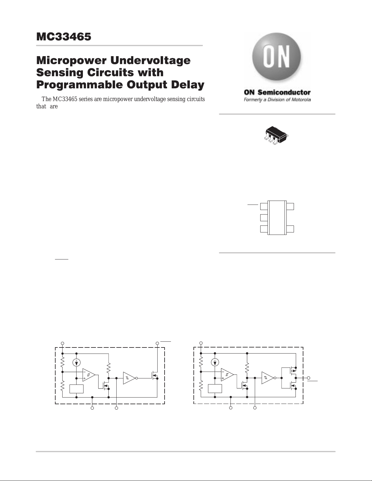
The MC33465 series features a highly accurate voltage reference, a
comparator with precise thresholds and built–in hysteresis to prevent
erratic reset operation, a choice of output configurations between open
drain or complementary, a time delayed output, which can be
programmed by the system designer, and guaranteed operation below
1.0 V with extremely low standby current. This device is available in a
SOT–23 5–pin surface mount package.
Applications include direct monitoring of the MPU/logic power
supply used in appliance, automotive, industrial and portable
equipment.
Features:
• Extremely Low Standby Current of 1.0 µA at V
• Wide Input Voltage Range (0.7 V to 10 V)
• Monitors Power Supply Voltages from 1.1 V to 5.0 V
• High Accuracy Detector Threshold (±2.5%)
• T wo Reset Output Types (Open Drain or Complementary Drive)
• Programmable Output Delay by External Capacitor
(100 ms typ. with 0.15 µF)
• Surface Mount Package (SOT–23 5–Pin)
• Convenient Tape and Reel (3000 per Reel)
= 3.5 V
in
http://onsemi.com
5
1
SOT–23–5
N SUFFIX
CASE 1212
PIN CONNECTIONS
15
Reset
2
Input
Ground
3
(Top View)
ORDERING INFORMATION
See detailed ordering and shipping information in the package
dimensions section on page 7 of this data sheet.
C
D
N/C
4
MC33465N–YYATR
Open Drain Output Configuration
2 Input
R
D
V
ref
3 Gnd
Semiconductor Components Industries, LLC, 1999
October, 1999 – Rev. 3
5C
Representative Block Diagrams
Complementary Output Configuration
1 Reset
D
YY Denotes Threshold Voltage
This device contains 28 active transistors.
2 Input
1 Publication Order Number:
MC33465N–YYCTR
V
ref
3 Gnd 5C
R
D
D
1
Reset
MC33465/D
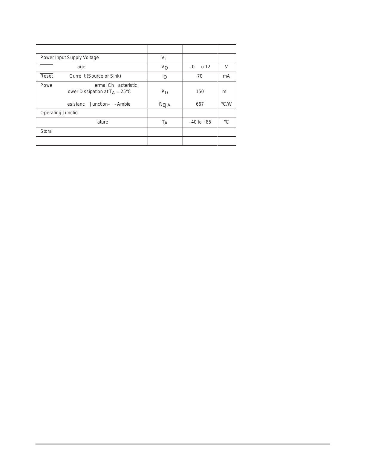
MAXIMUM RATINGS
Rating Symbol Value Unit
Power Input Supply Voltage
Reset Output Voltage
Reset Output Current (Source or Sink)
Power Dissipation and Thermal Characteristics
Maximum Power Dissipation at TA = 25°C P
Case 1212 (SOT–23) N Suffix
Thermal Resistance, Junction–to–Ambient R
Operating Junction Temperature
Operating Ambient Temperature
Storage Temperature Range
Lead Temperature (Soldering)
MC33465
V
in
V
O
I
O
D
θJA
T
J
T
A
T
stg
T
solder
0 to 12
–0.3 to 12
70
150 mW
667 °C/W
+125
–40 to +85
–40 to +125
260°C, 10 s
V
V
mA
°C
°C
°C
http://onsemi.com
2
MC33465
ELECTRICAL CHARACTERISTICS (For all values T
Characteristic
SENSE COMPARATOR
Threshold Voltage
High to Low State Output (Vin Decreasing) V
09 Suffix 0.878 0.9 0.922
20 Suffix 1.950 2.0 2.050
22 Suffix 2.145 2.2 2.255
27 Suffix 2.633 2.7 2.767
28 Suffix 2.730 2.8 2.870
30 Suffix 2.925 3.0 3.075
32 Suffix 3.120 3.2 3.280
34 Suffix 3.315 3.4 3.485
38 Suffix 3.705 3.8 3.895
43 Suffix 4.193 4.3 4.407
44 Suffix 4.290 4.4 4.510
45 Suffix 4.387 4.5 4.612
46 Suffix 4.485 4.6 4.715
47 Suffix 4.583 4.7 4.817
Threshold Hysteresis (Vin Increasing) V
09 Suffix 0.027 0.045 0.063
20 Suffix 0.060 0.100 0.140
22 Suffix 0.066 0.110 0.154
27 Suffix 0.081 0.135 0.189
28 Suffix 0.084 0.140 0.196
30 Suffix 0.090 0.150 0.210
32 Suffix 0.096 0.160 0.224
34 Suffix 0.102 0.170 0.238
38 Suffix 0.114 0.190 0.266
43 Suffix 0.129 0.215 0.301
44 Suffix 0.132 0.220 0.308
45 Suffix 0.135 0.225 0.315
46 Suffix 0.138 0.230 0.322
47 Suffix 0.141 0.235 0.329
Threshold Voltage Temperature Coefficient
RESET OUTPUT
Output Voltage
High State (Complementary Output: I
Low State (Complementary or Open Drain Output: I
Output Sink Current (Vin = 1.5 V, VOL = 0.5 V)
Output Source Current (Vin = 4.5 V, VOH = 2.4 V)
DELAY OUTPUT
Output Sink Current (Vin = 1.5 V, VOL = 0.5 V)
Delay Resistance
TOTAL DEVICE
Operating Input Voltage Range
Quiescent Input Current
Vin = 4.34 V – 5.5 11
Vin = 6.50 V – 1.3 3.9
NOTE: 1.Low duty pulse techniques are used during test to maintain junction temperature as close to ambient as possible.
= 1.0 mA) V
source
= 25°C (Note 1), unless otherwise noted.)
A
Symbol Min Typ Max Unit
IL
H
T
C
I
OL
I
OH
I
OL
R
V
I
OH
OL
D
in
in
= 1.0 mA) V
sink
–
Vin – 2.1 Vin – 1.0 V
– 0.25 0.5
1.0
1.0
0.2
0.5
0.8 to 10
±100
2.0
2.0
0.8
1.0
–
2.0
V
V
–
–
–
–
–
PPM/°C
V
in
mA
mA
mA
MΩ
V
µA
http://onsemi.com
3
 Loading...