


Motorola MC33179D, MC33179DR2, MC33178D, MC33178DR2, MC33179P Datasheet
...Order this document by MC33178/D
|
|
MC33178 |
|
High Output |
Current |
MC33179 |
|
|
|||
Low Power, Low Noise Bipolar |
|||
Operational |
Amplifiers |
HIGH OUTPUT CURRENT |
|
The MC33178/9 series is a family of high quality monolithic amplifiers |
|||
LOW POWER, LOW NOISE |
|||
employing Bipolar technology with innovative high performance concepts for |
|||
quality audio and data signal processing applications. This device family |
OPERATIONAL AMPLIFIERS |
||
incorporates the use of high frequency PNP input transistors to produce |
|||
|
|||
amplifiers exhibiting low input offset voltage, noise and distortion. In addition, |
|
||
the amplifier provides high output current drive capability while consuming |
|
||
only 420 μA of drain current per amplifier. The NPN output stage used, |
DUAL |
||
exhibits no deadband crossover distortion, large output voltage swing, |
|||
|
|||
excellent phase and gain margins, low open±loop high frequency output |
P SUFFIX |
||
impedance, symmetrical source and sink AC frequency performance. |
|||
The MC33178/9 family offers both dual and quad amplifier versions, |
PLASTIC PACKAGE |
||
CASE 626 |
|||
tested over the vehicular temperature range, and are available in DIP and |
|||
8 |
|||
SOIC packages. |
|
1 |
|
• 600 Ω Output Drive Capability |
|
|
|
|
|
|
D SUFFIX |
||||||
• Large Output Voltage Swing |
|
|
|
|
|
|
|||||||
|
|
|
|
|
|
PLASTIC PACKAGE |
|||||||
• Low Offset Voltage: 0.15 mV (Mean) |
|
|
8 |
|
|
||||||||
|
|
|
|
CASE 751 |
|||||||||
|
|
1 |
|
|
|||||||||
• Low T.C. of Input Offset Voltage: 2.0 μV/°C |
|
|
|
|
|
(SO±8) |
|||||||
|
|
|
|
|
|
||||||||
|
|
|
|
|
|
|
|
|
|||||
• Low Total Harmonic Distortion: 0.0024% (@ 1.0 kHz w/600 Ω Load) |
PIN CONNECTIONS |
|
|||||||||||
• High Gain Bandwidth: 5.0 MHz |
|
|
|
|
|||||||||
|
|
|
|
|
|
|
|
|
|
||||
• |
|
μ |
|
|
|
Output 1 |
1 |
|
8 |
V |
|
||
• |
High Slew Rate: 2.0 V/ |
s |
|
|
|
|
|
|
|
|
CC |
|
|
Dual Supply Operation: |
± |
± |
|
|
|
|
2 |
± |
7 |
Output 2 |
|||
|
2.0 V to 18 V |
|
|
Inputs 1 |
|
+ |
|
|
|
||||
• ESD Clamps on the Inputs Increase Ruggedness |
|
3 |
6 |
|
|
||||||||
|
|
|
± |
Inputs 2 |
|||||||||
|
|
without Affecting Device Performance |
|
|
VEE 4 |
+ |
5 |
|
|
||||
|
|
|
|
|
|
|
|||||||
|
|
|
|
|
|
|
|
|
|
(Top View) |
|
|
|
|
Representative Schematic Diagram (Each Amplifier) |
|
|
|
|
|
|
|
|||||
|
VCC |
|
|
|
|
|
|
|
|
QUAD |
|
|
|
|
|
|
|
|
|
|
|
|
|
|
|
|
|
|
|
|
|
|
Iref |
|
|
|
|
|
P SUFFIX |
||
|
|
|
|
|
|
|
|
|
PLASTIC PACKAGE |
||||
|
|
Iref |
|
|
|
|
|
|
|
||||
|
|
|
|
|
|
14 |
|
|
|
CASE 646 |
|||
|
|
|
|
|
|
|
1 |
|
|
|
|
|
|
|
V ± |
|
|
V + |
CC |
|
|
|
|
|
|
|
|
|
in |
|
|
in |
|
|
|
|
|
|
D SUFFIX |
||
|
|
|
|
|
|
|
|
|
|
|
|||
|
|
|
|
|
|
VO |
|
|
|
PLASTIC PACKAGE |
|||
|
|
|
|
|
CM |
14 |
|
|
|
CASE 751A |
|||
|
|
|
|
|
|
|
|
|
|||||
|
|
|
|
|
|
|
|
|
|
(SO±14) |
|||
|
|
|
|
|
|
1 |
|
|
|
|
|||
|
|
|
|
|
|
|
|
|
|
|
|||
|
|
|
|
|
|
|
PIN CONNECTIONS |
|
|||||
|
VEE |
|
|
|
|
|
Output 1 |
1 |
|
|
|
14 |
Output 4 |
|
|
|
|
|
|
|
|
|
|
|
|
|
|
|
|
ORDERING INFORMATION |
|
Inputs 1 |
2 |
± |
|
4 ± |
13 |
Inputs 4 |
|||
|
|
|
|
1 |
|
||||||||
|
Op Amp |
Fully |
|
Operating |
|
|
3 |
+ |
|
+ |
12 |
|
|
|
|
|
V |
|
|
|
|
|
V |
||||
|
Function |
Compensated |
Temperature Range |
Package |
4 |
|
|
|
11 |
||||
|
CC |
|
|
|
|
|
EE |
||||||
|
Dual |
MC33178D |
|
|
SO±8 |
Inputs 2 |
5 |
+ |
|
+ |
10 |
Inputs 3 |
|
|
|
|
|
2 |
|
||||||||
|
|
MC33178P |
|
|
Plastic DIP |
|
|
3 |
|
||||
|
|
TA = ±40° to +85°C |
|
6 |
± |
|
± |
9 |
|
||||
|
Quad |
MC33179D |
SO±14 |
Output 2 |
7 |
|
|
|
8 |
Output 3 |
|||
|
|
|
|
|
|
||||||||
|
|
MC33179P |
|
|
Plastic DIP |
|
|
|
|
|
|
|
|
|
|
|
|
|
|
|
|
|
|
(Top View) |
|
|
|
Motorola, Inc. 1996 |
Rev 0 |

MC33178 MC33179
MAXIMUM RATINGS
Rating |
Symbol |
Value |
Unit |
|
|
|
|
Supply Voltage (VCC to VEE) |
VS |
+36 |
V |
Input Differential Voltage Range |
VIDR |
(Note 1) |
V |
Input Voltage Range |
VIR |
(Note 1) |
V |
Output Short Circuit Duration (Note 2) |
tSC |
Indefinite |
sec |
Maximum Junction Temperature |
TJ |
+150 |
°C |
Storage Temperature Range |
Tstg |
±60 to +150 |
°C |
Maximum Power Dissipation |
PD |
(Note 2) |
mW |
NOTES: 1. Either or both input voltages should not exceed VCC or VEE.
2.Power dissipation must be considered to ensure maximum junction temperature (TJ) is not exceeded. (See power dissipation performance characteristic, Figure 1.)
DC ELECTRICAL CHARACTERISTICS (VCC = +15 V, VEE = ±15 V, TA = 25°C, unless otherwise noted.)
Characteristics |
Figure |
Symbol |
Min |
Typ |
Max |
Unit |
|
|
|
|
|
|
|
Input Offset Voltage (RS = 50 Ω, VCM = 0 V, VO = 0 V) |
2 |
|VIO| |
|
|
|
mV |
(VCC = +2.5 V, VEE = ±2.5 V to VCC = +15 V, VEE = ±15 V) |
|
|
|
|
|
|
TA = +25°C |
|
|
Ð |
0.15 |
3.0 |
|
TA = ±40° to +85°C |
|
|
Ð |
Ð |
4.0 |
|
Average Temperature Coefficient of Input Offset Voltage |
2 |
VIO/ T |
|
|
|
μV/°C |
(RS = 50 Ω, VCM = 0 V, VO = 0 V) |
|
|
|
|
|
|
TA = ±40° to +85°C |
|
|
Ð |
2.0 |
Ð |
|
Input Bias Current (VCM = 0 V, VO = 0 V) |
3, 4 |
IIB |
|
|
|
nA |
TA = +25°C |
|
|
Ð |
100 |
500 |
|
TA = ±40° to +85°C |
|
|
Ð |
Ð |
600 |
|
Input Offset Current (VCM = 0 V, VO = 0 V) |
|
|IIO| |
|
|
|
nA |
TA = +25°C |
|
|
Ð |
5.0 |
50 |
|
TA = ±40° to +85°C |
|
|
Ð |
Ð |
60 |
|
Common Mode Input Voltage Range |
5 |
VICR |
±13 |
±14 |
Ð |
V |
( VIO = 5.0 mV, VO = 0 V) |
|
|
Ð |
+14 |
+13 |
|
Large Signal Voltage Gain (VO = ±10 V to +10 V, RL = 600 Ω) |
6, 7 |
AVOL |
|
|
|
V/V |
TA = +25°C |
|
|
50 k |
200 k |
Ð |
|
TA = ±40° to +85°C |
|
|
25 k |
Ð |
Ð |
|
Output Voltage Swing (VID = ±1.0 V) |
8, 9, 10 |
|
|
|
|
V |
(VCC = +15 V, VEE = ±15 V) |
|
|
|
|
|
|
RL = 300 Ω |
|
VO+ |
Ð |
+12 |
Ð |
|
RL = 300 Ω |
|
VO± |
Ð |
±12 |
Ð |
|
RL = 600 Ω |
|
VO+ |
+12 |
+13.6 |
Ð |
|
RL = 600 Ω |
|
VO± |
Ð |
±13 |
±12 |
|
RL = 2.0 kΩ |
|
VO+ |
+13 |
+14 |
Ð |
|
RL = 2.0 kΩ |
|
VO± |
Ð |
±13.8 |
±13 |
|
(VCC = +2.5 V, VEE = ±2.5 V) |
|
|
|
|
|
|
RL = 600 Ω |
|
VO+ |
1.1 |
1.6 |
Ð |
|
RL = 600 Ω |
|
VO± |
Ð |
±1.6 |
±1.1 |
|
Common Mode Rejection (Vin = ±13 V) |
11 |
CMR |
80 |
110 |
Ð |
dB |
Power Supply Rejection |
12 |
PSR |
80 |
110 |
Ð |
dB |
VCC/VEE = +15 V/ ±15 V, +5.0 V/ ±15 V, +15 V/ ±5.0 V |
|
|
|
|
|
|
Output Short Circuit Current (VID = ±1.0 V, Output to Ground) |
13, 14 |
ISC |
|
|
|
mA |
Source (VCC = 2.5 V to 15 V) |
|
|
+50 |
+80 |
Ð |
|
Sink (VEE = ±2.5 V to ±15 V) |
|
|
±50 |
±100 |
Ð |
|
Power Supply Current (VO = 0 V) |
15 |
ID |
|
|
|
mA |
(VCC = 2.5 V, VEE = ±2.5 V to VCC = +15 V, VEE = ±15 V) |
|
|
|
|
|
|
MC33178 (Dual) |
|
|
|
|
|
|
TA = +25°C |
|
|
Ð |
Ð |
1.4 |
|
TA = ±40° to +85°C |
|
|
Ð |
Ð |
1.6 |
|
MC33179 (Quad) |
|
|
|
|
|
|
TA = +25°C |
|
|
Ð |
1.7 |
2.4 |
|
TA = ±40° to +85°C |
|
|
Ð |
Ð |
2.6 |
|
2 |
MOTOROLA ANALOG IC DEVICE DATA |
MC33178 MC33179
AC ELECTRICAL CHARACTERISTICS (VCC = +15 V, VEE = ±15 V, TA = 25°C, unless otherwise noted.)
Characteristics |
Figure |
Symbol |
Min |
Typ |
Max |
Unit |
||||
|
|
|
|
|
|
|
|
|
|
|
Slew Rate |
16, 31 |
SR |
1.2 |
2.0 |
Ð |
V/μs |
||||
(Vin = ±10 V to +10 V, RL = 2.0 kΩ, CL = 100 pF, AV = +1.0 V) |
|
|
|
|
|
|
|
|
|
|
Gain Bandwidth Product (f = 100 kHz) |
17 |
GBW |
2.5 |
5.0 |
Ð |
MHz |
||||
|
|
|
|
|
|
|
|
|
|
|
AC Voltage Gain (RL = 600 Ω, VO = 0 V, f = 20 kHz) |
18, 19 |
AVO |
Ð |
50 |
Ð |
dB |
||||
Unity Gain Frequency (Open±Loop) (RL = 600 Ω, CL = 0 pF) |
|
fU |
Ð |
3.0 |
Ð |
MHz |
||||
Gain Margin (RL = 600 Ω, CL = 0 pF) |
20, 22, 23 |
Am |
Ð |
15 |
Ð |
dB |
||||
Phase Margin (RL = 600 Ω, CL = 0 pF) |
21, 22, 23 |
φm |
Ð |
60 |
Ð |
Degree |
||||
|
|
|
|
|
|
s |
||||
|
|
|
|
|
|
|
|
|
|
|
Channel Separation (f = 100 Hz to 20 kHz) |
24 |
CS |
Ð |
±120 |
Ð |
dB |
||||
|
|
|
|
|
|
|
|
|
|
|
Power Bandwidth (VO = 20 Vpp, RL = 600 Ω, THD ≤ 1.0%) |
|
BWp |
Ð |
32 |
Ð |
kHz |
||||
Distortion (RL = 600 Ω,, VO = 2.0 Vpp, AV = +1.0 V) |
25 |
THD |
|
|
|
% |
|
|
|
|
(f = 1.0 kHz) |
|
|
Ð |
0.0024 |
Ð |
|
|
|
|
|
(f = 10 kHz) |
|
|
Ð |
0.014 |
Ð |
|
|
|
|
|
(f = 20 kHz) |
|
|
Ð |
0.024 |
Ð |
|
|
|
|
|
|
|
|
|
|
|
|
|
|
|
|
Open Loop Output Impedance |
26 |
|ZO| |
Ð |
150 |
Ð |
Ω |
||||
(VO = 0 V, f = 3.0 MHz, AV = 10 V) |
|
|
|
|
|
|
|
|
|
|
Differential Input Resistance (VCM = 0 V) |
|
Rin |
Ð |
200 |
Ð |
kΩ |
||||
Differential Input Capacitance (VCM = 0 V) |
|
Cin |
Ð |
10 |
Ð |
pF |
||||
Equivalent Input Noise Voltage (RS = 100 Ω,) |
27 |
en |
|
|
|
nV/√ |
|
|
|
|
|
|
|
Hz |
|||||||
f = 10 Hz |
|
|
Ð |
8.0 |
Ð |
|
|
|
|
|
f = 1.0 kHz |
|
|
Ð |
7.5 |
Ð |
|
|
|
|
|
|
|
|
|
|
|
|
|
|
||
Equivalent Input Noise Current |
28 |
in |
|
|
|
pA/ √ |
|
|
||
|
|
|
Hz |
|||||||
f = 10 Hz |
|
|
Ð |
0.33 |
Ð |
|
|
|
|
|
f = 1.0 kHz |
|
|
Ð |
0.15 |
Ð |
|
|
|
|
|
|
|
|
|
|
|
|
|
|
|
|
Figure 1. Maximum Power Dissipation |
Figure 2. Input Offset Voltage versus |
(mW) |
|
|
|
|
|
versus Temperature |
|
|
|
|
|
|
Temperature for 3 Typical Units |
|
|
||||||||
|
|
|
|
|
|
|
|
|
|
|
|
|
|
||||||||||
DISSIPATIONPOWERMAXIMUM |
2400 |
|
|
|
|
|
|
|
|
|
|
|
|
|
(mV)VOLTAGEOFFSETINPUT |
4.0 |
|
|
|
|
|
|
|
|
|
|
|
|
|
|
|
|
|
|
|
|
|
3.0 |
|
|
|
|
VCC |
= +15 V |
|
||
|
2000 |
|
MC33178P/9P |
|
|
|
|
|
|
|
|
|
|
|
|
|
|
VEE = ±15 V |
|
||||
|
|
|
|
|
|
|
|
|
|
|
|
|
|
|
|
|
|
||||||
|
|
|
|
|
|
|
|
|
|
|
|
|
|
|
|
2.0 |
|
|
|
|
RS = 10 Ω |
|
|
|
|
|
|
|
|
|
|
|
|
|
|
|
|
|
|
|
|
Unit 1 |
|
VCM |
= 0 V |
|
|
|
1600 |
|
|
|
|
|
|
|
|
|
|
|
|
|
|
|
|
|
|
|
|||
|
|
|
|
|
|
|
|
|
|
|
|
|
|
|
1.0 |
|
|
|
|
|
|
|
|
|
|
|
MC33179D |
|
|
|
|
|
|
|
|
|
|
|
|
|
Unit 2 |
|
|
|
|
||
|
|
|
|
|
|
|
|
|
|
|
|
|
|
|
|
|
|
|
|
|
|||
|
1200 |
|
|
|
|
|
|
|
|
|
|
|
|
|
|
0 |
|
|
|
|
|
|
|
|
|
|
|
|
|
|
|
|
|
|
|
|
|
|
|
|
Unit 3 |
|
|
|
|
||
|
|
|
|
|
|
|
|
|
|
|
|
|
|
|
|
±1.0 |
|
|
|
|
|
|
|
|
800 |
MC33178D |
|
|
|
|
|
|
|
|
|
|
|
|
|
|
|
|
|
|
|||
|
|
|
|
|
|
|
|
|
|
|
|
|
|
|
|
|
|
|
|
||||
(MAX), |
|
|
|
|
|
|
|
|
|
|
|
|
|
|
V |
±2.0 |
|
|
|
|
|
|
|
400 |
|
|
|
|
|
|
|
|
|
|
|
|
|
|
|
|
|
|
|
|
|
||
|
|
|
|
|
|
|
|
|
|
|
|
|
|
, |
|
|
|
|
|
|
|
|
|
|
|
|
|
|
|
|
|
|
|
|
|
|
|
|
IO |
±3.0 |
|
|
|
|
|
|
|
D |
0 |
|
|
|
|
|
|
|
|
|
|
|
|
|
|
±4.0 |
|
|
|
|
|
|
|
P |
|
±40 |
±20 |
0 |
20 |
40 |
60 |
80 |
100 |
120 |
140 |
160 |
180 |
|
±25 |
0 |
25 |
50 |
75 |
100 |
125 |
||
|
±60 |
|
±55 |
||||||||||||||||||||
|
|
|
|
|
TA, AMBIENT TEMPERATURE (°C) |
|
|
|
|
|
|
TA, AMBIENT TEMPERATURE (°C) |
|
|
|||||||||
MOTOROLA ANALOG IC DEVICE DATA |
3 |
|

MC33178 MC33179
I IB, INPUT BIAS CURRENT (nA)
Figure 3. Input Bias Current |
Figure 4. Input Bias Current |
versus Common Mode Voltage |
versus Temperature |
160 |
|
|
|
|
|
|
|
120 |
|
|
|
|
|
|
|
140 |
|
|
|
|
|
|
(nA) |
110 |
VCC = +15 V |
|
|
|
|
|
|
|
|
|
|
|
|
|
|
|
|
|
|
|
|||
120 |
|
|
|
|
|
|
|
VEE = ±15 V |
|
|
|
|
|
|
|
|
|
|
|
|
|
CURRENT |
|
|
|
|
|
|
|
||
|
|
|
|
|
|
|
VCM = 0 V |
|
|
|
|
|
|
||
|
|
|
|
|
|
|
100 |
|
|
|
|
|
|
||
|
|
|
|
|
|
|
|
|
|
|
|
|
|
||
100 |
|
|
|
|
|
|
|
|
|
|
|
|
|
|
|
|
|
|
|
|
|
|
|
|
|
|
|
|
|
|
|
80 |
|
|
|
|
|
|
BIAS |
90 |
|
|
|
|
|
|
|
60 |
VCC = +15 V |
|
|
|
|
|
|
|
|
|
|
|
|
|
|
|
|
|
|
|
INPUT, |
80 |
|
|
|
|
|
|
|
||
40 |
TA = 25°C |
|
|
|
|
|
|
|
|
|
|
|
|
||
|
VEE = ±15 V |
|
|
|
|
|
|
|
|
|
|
|
|
|
|
|
|
|
|
|
|
|
IB |
70 |
|
|
|
|
|
|
|
20 |
|
|
|
|
|
|
I |
|
|
|
|
|
|
|
|
|
|
|
|
|
|
|
|
|
|
|
|
|
|
|
|
0 |
±10 |
±5.0 |
0 |
5.0 |
10 |
15 |
|
60 |
±25 |
0 |
25 |
50 |
75 |
100 |
125 |
±15 |
|
±55 |
|||||||||||||
|
VCM, COMMON MODE VOLTAGE (V) |
|
|
|
|
TA, AMBIENT TEMPERATURE (°C) |
|
|
|||||||
(V)
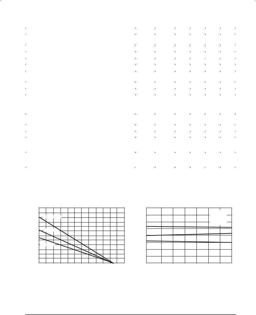
Figure 5. Input Common Mode Voltage |
Figure 6. Open Loop Voltage Gain |
Range versus Temperature |
versus Temperature |
COMMON MODE VOLTAGERANGE |
VCC |
|
|
|
|
|
|
,OPEN LOOP VOLTAGE GAIN (kV/V) |
250 |
|
|
|
|
|
|
|
VCC ±0.5 V |
|
|
|
|
|
|
200 |
|
|
|
|
|
|
|
||
VCC ±1.0 V |
|
|
|
VCC = +5.0 V to +18 V |
|
|
|
|
|
|
|
|||||
|
|
|
|
|
|
|
|
|
|
|
||||||
VCC ±1.5 V |
|
|
|
VEE = ±5.0 V to ±18 V |
|
|
|
|
|
|
|
|
||||
|
|
|
|
VIO = 5.0 mV |
|
150 |
|
|
|
|
|
|
|
|||
VCC ±2.0 V |
|
|
|
|
|
|
|
VCC = +15 V |
|
|
|
|
|
|
||
|
|
|
|
|
|
|
100 |
|
|
|
|
|
|
|||
|
|
|
|
|
|
|
|
VEE = ±15 V |
|
|
|
|
|
|
||
VEE +1.0 V |
|
|
|
|
|
|
|
f = 10 Hz |
|
|
|
|
|
|
||
|
|
|
|
|
|
50 |
VO = 10 V to +10 V |
|
|
|
|
|
||||
VEE +0.5 V |
|
|
|
|
|
|
RL = 600 Ω |
|
|
|
|
|
|
|||
INPUT, |
|
|
|
|
|
|
VOL |
|
|
|
|
|
|
|
|
|
|
|
|
|
|
|
|
|
|
|
|
|
|
|
|
||
ICR |
VEE |
±25 |
0 |
25 |
50 |
75 |
100 |
A |
0 |
±25 |
0 |
25 |
50 |
75 |
100 |
125 |
V |
±55 |
125 |
±55 |
|||||||||||||
|
|
|
TA, AMBIENT TEMPERATURE (°C) |
|
|
|
TA, AMBIENT TEMPERATURE (°C) |
|
|
|||||||
Figure 7. Voltage Gain and Phase |
Figure 8. Output Voltage Swing |
|
|
|
|
|
versus Frequency |
|
|
|
|
versus Supply Voltage |
|
|||||||
(dB) |
50 |
|
|
|
|
|
|
|
|
|
80 |
|
|
40 |
|
|
|
|
40 |
|
|
|
|
|
|
|
|
VCC = +15 V |
100 |
|
|
|
|
|
|
|
|
,OPEN LOOP VOLTAGE GAIN |
|
|
|
|
|
|
|
|
EXCESS PHASE (DEGREES) |
|
35 |
|
|
|
|
|||
30 |
|
|
|
|
|
|
|
|
VEE = ±15 V |
120 |
) |
30 |
TA = 25°C |
|
|
|
||
|
|
|
|
|
|
|
|
|
VO = 0 V |
|
pp |
|
|
|
|
|||
20 |
|
|
|
|
|
|
|
|
TA = 25°C |
140 |
,OUTPUT VOLTAGE (V |
25 |
|
RL = 10 kΩ |
|
|
||
10 |
|
|
|
|
|
|
|
|
|
160 |
|
|
RL = 600 Ω |
|
||||
|
|
|
|
|
|
|
|
|
|
|
|
|
||||||
0 |
|
|
|
|
|
|
|
|
|
180 |
20 |
|
|
|
||||
|
|
|
|
|
|
|
|
1A |
|
|
|
|
||||||
±10 |
|
|
|
|
|
|
|
|
200 |
|
|
|
|
|
||||
|
|
|
|
|
|
|
|
1B |
15 |
|
|
|
|
|||||
±20 |
|
|
|
|
|
|
|
|
|
|
|
|
|
|||||
|
|
|
|
|
|
|
|
220 |
|
|
|
|
|
|||||
1A) Phase (RL = 600 Ω) |
|
|
|
|
2B |
10 |
|
|
|
|
||||||||
±30 |
|
|
|
|
|
|
|
|
|
|||||||||
2A) Phase (R |
|
= 600 Ω, C |
|
= 300 pF) |
|
|
240 |
|
|
|
|
|
||||||
VOL |
L |
L |
|
2A |
, |
O |
5.0 |
|
|
|
|
|||||||
|
|
|
Ω |
|
|
|
|
|
|
|
|
|||||||
A |
±40 |
1B) Gain (RL = 600 |
) |
|
|
|
|
|
260 |
φ |
V |
|
|
|
|
|
||
2B) Gain (RL = 600 Ω, CL = 300 pF) |
|
|
0 |
|
|
|
|
|||||||||||
|
±50 |
|
3 |
4 |
5 |
|
6 |
7 |
8 |
9 10 |
20280 |
|
|
5.0 |
10 |
15 |
20 |
|
|
2 |
|
|
|
|
0 |
||||||||||||
|
|
|
|
|
f, FREQUENCY (Hz) |
|
|
|
|
VCC, |VEE|, SUPPLY VOLTAGE (V) |
|
|||||||
4 |
MOTOROLA ANALOG IC DEVICE DATA |
 Loading...