


Motorola MC34025DW, MC34025DWR2, MC34025P, MC33025DW, MC33025DWR2 Datasheet
...High Speed Double-Ended
PWM Controller
The MC34025 series are high speed, fixed frequency, double±ended pulse width modulator controllers optimized for high frequency operation. They are specifically designed for Off±Line and DC±to±DC converter applications offering the designer a cost effective solution with minimal external components. These integrated circuits feature an oscillator, a temperature compensated reference, a wide bandwidth error amplifier, a high speed current sensing comparator, steering flip±flop, and dual high current totem pole outputs ideally suited for driving power MOSFETs.
Also included are protective features consisting of input and reference undervoltage lockouts each with hysteresis, cycle±by±cycle current limiting, and a latch for single pulse metering.
The flexibility of this series allows it to be easily configured for either current mode or voltage mode control.
•50 ns Propagation Delay to Outputs
•Dual High Current Totem Pole Outputs
•Wide Bandwidth Error Amplifier
•Fully±Latched Logic with Double Pulse Suppression
•Latching PWM for Cycle±By±Cycle Current Limiting
•Soft±Start Control with Latched Overcurrent Reset
•Input Undervoltage Lockout with Hysteresis
•Low Start±Up Current (500 μA Typ)
•Internally Trimmed Reference with Undervoltage Lockout
•90% Maximum Duty Cycle (Externally Adjustable)
•Precision Trimmed Oscillator
•Voltage or Current Mode Operation to 1.0 MHz
•Functionally Similar to the UC3825
|
|
Simplified |
Application |
|
|
Vref |
16 |
|
5.1V |
15 |
|
|
|
|
|||
4 |
|
Reference |
VCC |
||
|
|
||||
Clock |
|
|
|||
|
|
|
|
||
RT |
5 |
|
UVLO |
|
|
|
Oscillator |
|
13 |
||
CT |
|
|
|||
6 |
|
|
VC |
||
|
|
|
14 |
||
|
7 |
|
|
||
Ramp |
|
|
Output B |
||
3 |
|
Latching |
|||
Error Amp |
|
PWM and |
|
||
Output |
|
Error |
Steering |
11 |
|
Noninverting |
2 |
Flip Flop |
|||
Amp |
|||||
Input |
|
|
Output A |
||
|
|
|
|||
|
|
|
Power |
||
Inverting |
|
|
|
||
Input |
1 |
|
|
12 Ground |
|
|
8 |
|
|
9 |
|
Soft±Start |
|
Soft±Star |
|
Current |
|
|
|
t |
|
Limit/ |
|
|
|
|
|
Shutdown |
|
|
|
|
10 Ground |
|
This device contains 227 active transistors.
Order this document by MC34025/D
MC34025
MC33025
16
1
P SUFFIX
PLASTIC PACKAGE
CASE 648
16 
1
DW SUFFIX
PLASTIC PACKAGE
CASE 751G
(SO±16L)
PIN CONNECTIONS
Error Amp |
|
|
|
|
|
|
|
Inverting Input |
1 |
|
|
|
16 |
V |
|
Error Amp |
|
|
|
|
|
|
ref |
|
|
|
|
|
|
|
|
2 |
|
|
|
|
15 |
V |
|
Noninverting Input |
|
|
|
|
|
|
CC |
|
|
|
|
|
|
|
|
Error Amp Output |
3 |
|
|
|
|
14 |
Output B |
|
|
|
|
|
|
|
|
Clock |
4 |
|
|
|
|
13 |
V |
|
|
|
|
|
|
|
C |
|
|
|
|
|
|
|
|
R |
5 |
|
|
|
|
12 |
Power Ground |
T |
|
|
|
|
|
|
|
CT |
6 |
|
|
|
11 |
Output A |
|
|
|
|
|
|
|
|
|
Ramp |
7 |
|
|
|
|
10 |
Ground |
|
|
|
|
|
|
|
Current Limit/ |
Soft±Start |
8 |
|
|
|
|
9 |
|
|
|
|
Shutdown |
||||
|
|
|
|
|
|
|
|
|
|
(Top View) |
|
||||
ORDERING INFORMATION
|
Operating |
|
|
Device |
Temperature Range |
Package |
|
|
|
|
|
MC33025DW |
TA = ± 40° to +105°C |
SO±16L |
|
|
|
||
MC33025P |
Plastic DIP |
||
|
|||
|
|
|
|
MC34025DW |
TA = 0° to +70°C |
SO±16L |
|
|
|
||
MC34025P |
Plastic DIP |
||
|
|||
|
|
|
Motorola, Inc. 1996 |
Rev 1 |

MC34025 MC33025
MAXIMUM RATINGS
Rating |
Symbol |
Value |
Unit |
|
|
|
|
Power Supply Voltage |
VCC |
30 |
V |
Output Driver Supply Voltage |
VC |
20 |
V |
Output Current, Source or Sink (Note 1) |
IO |
|
A |
DC |
|
0.5 |
|
Pulsed (0.5 μs) |
|
2.0 |
|
|
|
|
|
Current Sense, Soft±Start, Ramp, and Error Amp Inputs |
Vin |
± 0.3 to +7.0 |
V |
Error Amp Output and Soft±Start Sink Current |
IO |
10 |
mA |
Clock and RT Output Current |
ICO |
5.0 |
mA |
Power Dissipation and Thermal Characteristics |
|
|
|
SO±16 Package (Case 751G) |
|
|
|
Maximum Power Dissipation @ TA = + 25°C |
PD |
862 |
mW |
Thermal Resistance, Junction±to±Air |
RθJA |
145 |
°C/W |
DIP Package (Case 648) |
|
|
|
Maximum Power Dissipation @ TA = + 25°C |
PD |
1.25 |
W |
Thermal Resistance, Junction±to±Air |
RθJA |
100 |
°C/W |
Operating Junction Temperature |
TJ |
+150 |
°C |
Operating Ambient Temperature (Note 2) |
|
|
°C |
MC34025 |
TA |
0 to +70 |
|
MC33025 |
|
± 40 to +105 |
|
|
|
|
|
Storage Temperature Range |
Tstg |
± 55 to +150 |
°C |
ELECTRICAL CHARACTERISTICS (VCC = 15 V, RT = 3.65 kΩ, CT = 1.0 nF, for typical values TA = + 25°C, for min/max values TA is the operating ambient temperature range that applies [Note 2], unless otherwise noted.)
Characteristic |
Symbol |
Min |
Typ |
Max |
Unit |
||
|
|
|
|
|
|
|
|
REFERENCE SECTION |
|
|
|
|
|
|
|
|
|
|
|
|
|
|
|
Reference Output Voltage (IO = 1.0 mA, TJ = + 25°C) |
Vref |
|
5.05 |
5.1 |
5.15 |
V |
|
Line Regulation (VCC = 10 V to 30 V) |
|
Regline |
± |
2.0 |
15 |
mV |
|
Load Regulation (IO = 1.0 mA to 10 mA) |
Regload |
± |
2.0 |
15 |
mV |
||
Temperature Stability |
|
TS |
|
± |
0.2 |
± |
mV/°C |
Total Output Variation over Line, Load, and Temperature |
Vref |
|
4.95 |
± |
5.25 |
V |
|
Output Noise Voltage (f = 10 Hz to 10 kHz, TJ = + 25°C) |
Vn |
|
± |
50 |
± |
μV |
|
Long Term Stability (TA = +125°C for 1000 Hours) |
S |
|
± |
5.0 |
± |
mV |
|
Output Short Circuit Current |
|
ISC |
|
±30 |
±65 |
±100 |
mA |
OSCILLATOR SECTION |
|
|
|
|
|
|
|
|
|
|
|
|
|
|
|
Frequency |
|
|
|
|
|
|
kHz |
TJ = + 25°C |
|
fosc |
|
380 |
400 |
420 |
|
Line (VCC = 10 V to 30 V) and Temperature (TA = Tlow to Thigh) |
|
|
370 |
400 |
430 |
|
|
Frequency Change with Voltage (VCC = 10 V to 30 V) |
fosc/ |
V |
± |
0.2 |
1.0 |
% |
|
Frequency Change with Temperature (TA = Tlow to Thigh) |
fosc/ |
T |
± |
2.0 |
± |
% |
|
Sawtooth Peak Voltage |
|
VP |
|
2.6 |
2.8 |
3.0 |
V |
Sawtooth Valley Voltage |
|
VV |
|
0.7 |
1.0 |
1.25 |
V |
Clock Output Voltage |
|
|
|
|
|
|
V |
High State |
|
VOH |
|
3.9 |
4.5 |
± |
|
Low State |
|
VOL |
|
± |
2.3 |
2.9 |
|
NOTES: 1. Maximum package power dissipation limits must be observed. |
|
|
|
|
|
|
|
2. Low duty cycle pulse techniques are used during test to maintain junction temperature as close to ambient as possible. |
|
|
|||||
Tlow = 0°C for MC34025 |
Thigh = +70°C for MC34025 |
|
|
|
|
|
|
= ± 40°C for MC33025 |
= +105°C for MC33025 |
|
|
|
|
|
|
2 |
MOTOROLA ANALOG IC DEVICE DATA |

MC34025 MC33025
ELECTRICAL CHARACTERISTICS (VCC = 15 V, RT = 3.65 kΩ, CT = 1.0 nF, for typical values TA = + 25°C, for min/max values TA is the operating ambient temperature range that applies [Note 2], unless otherwise noted.)
|
Characteristic |
Symbol |
Min |
Typ |
Max |
Unit |
|
|
|
|
|
|
|
|
|
ERROR AMPLIFIER SECTION |
|
|
|
|
|
|
|
|
|
|
|
|
|
|
|
Input Offset Voltage |
|
VIO |
± |
± |
15 |
mV |
|
Input Bias Current |
|
IIB |
± |
0.6 |
3.0 |
μA |
|
Input Offset Current |
|
IIO |
± |
0.1 |
1.0 |
μA |
|
Open±Loop Voltage Gain (VO = 1.0 V to 4.0 V) |
AVOL |
60 |
95 |
± |
dB |
||
Gain Bandwidth Product (TJ = + 25°C) |
|
GBW |
4.0 |
8.3 |
± |
MHz |
|
Common Mode Rejection Ratio (VCM = 1.5 V to 5.5 V) |
CMRR |
75 |
95 |
± |
dB |
||
Power Supply Rejection Ratio (VCC = 10 V to 30 V) |
PSRR |
85 |
110 |
± |
dB |
||
Output Current, Source (VO = 4.0 V) |
|
ISource |
0.5 |
3.0 |
± |
mA |
|
|
Sink (VO = 1.0 V) |
|
ISink |
1.0 |
3.6 |
± |
|
Output Voltage Swing, High State (IO = ± 0.5 mA) |
VOH |
4.5 |
4.75 |
5.0 |
V |
||
|
Low State (IO = 1.0 mA) |
VOL |
0 |
0.4 |
1.0 |
|
|
Slew Rate |
|
|
SR |
6.0 |
12 |
± |
V/μs |
|
|
|
|
|
|
|
|
PWM COMPARATOR SECTION |
|
|
|
|
|
|
|
|
|
|
|
|
|
|
|
Ramp Input Bias Current |
|
IIB |
± |
± 0.5 |
± 5.0 |
μA |
|
Duty Cycle, Maximum |
|
DC(max) |
80 |
90 |
± |
% |
|
Minimum |
|
DC(min) |
± |
± |
0 |
|
|
Zero Duty Cycle Threshold Voltage Pin 3(4) (Pin 7(9) = 0 V) |
Vth |
1.1 |
1.25 |
1.4 |
V |
||
Propagation Delay (Ramp Input to Output, TJ = + 25°C) |
tPLH(in/out) |
± |
60 |
100 |
ns |
||
SIFT±START SECTION |
|
|
|
|
|
|
|
|
|
|
|
|
|
|
|
Charge Current (VSoft±Start = 0.5 V) |
|
Ichg |
3.0 |
9.0 |
20 |
μA |
|
Discharge Current (VSoft±Start = 1.5 V) |
Idischg |
1.0 |
4.0 |
± |
mA |
||
CURRENT SENSE SECTION |
|
|
|
|
|
|
|
|
|
|
|
|
|
||
Input Bias Current (Pin 9(12) = 0 V to 4.0 V) |
IIB |
± |
± |
15 |
μA |
||
Current Limit Comparator Threshold |
|
Vth |
0.9 |
1.0 |
1.10 |
V |
|
Shutdown Comparator Threshold |
|
Vth |
1.25 |
1.40 |
1.55 |
|
|
Propagation Delay (Current Limit/Shutdown to Output, TJ = + 25°C) |
tPLH(in/out) |
± |
50 |
80 |
ns |
||
OUTPUT SECTION |
|
|
|
|
|
|
|
|
|
|
|
|
|
|
|
Output Voltage |
|
|
|
|
|
|
V |
Low State |
(ISink = 20 mA) |
|
VOL |
± |
0.25 |
0.4 |
|
|
(ISink = 200 mA) |
|
|
± |
1.2 |
2.2 |
|
High State |
(ISource = 20 mA) |
|
VOH |
13 |
13.5 |
± |
|
|
(ISource = 200 mA) |
|
|
12 |
13 |
± |
|
Output Voltage with UVLO Activated (VCC = 6.0 V, ISink = 0.5 mA) |
VOL(UVLO) |
± |
0.25 |
1.0 |
V |
||
Output Leakage Current (VC = 20 V) |
|
IL |
± |
100 |
500 |
μA |
|
Output Voltage Rise Time (CL = 1.0 nF, TJ = + 25°C) |
tr |
± |
30 |
60 |
ns |
||
Output Voltage Fall Time (CL = 1.0 nF, TJ = + 25°C) |
tf |
± |
30 |
60 |
ns |
||
UNDERVOLTAGE LOCKOUT SECTION |
|
|
|
|
|
||
|
|
|
|
|
|
|
|
Start±Up Threshold (VCC Increasing) |
|
Vth(on) |
8.8 |
9.2 |
9.6 |
V |
|
UVLO Hysteresis Voltage (VCC Decreasing After Turn±On) |
VH |
0.4 |
0.8 |
1.2 |
V |
||
TOTAL DEVICE |
|
|
|
|
|
|
|
|
|
|
|
|
|
|
|
Power Supply Current |
|
ICC |
|
|
|
mA |
|
Start±Up (VCC = 8.0 V) |
|
|
± |
0.5 |
1.2 |
|
|
Operating |
|
|
|
± |
25 |
35 |
|
|
|
|
|
|
|
||
NOTES: 1. Maximum package power dissipation limits must be observed. |
|
|
|
|
|
||
2. Low duty cycle pulse techniques are used during test to maintain junction temperature as close to ambient as possible. |
|
|
|||||
Tlow = 0°C for MC34025 |
Thigh = +70°C for MC34025 |
|
|
|
|
|
|
= ± 40°C for MC33025 |
= +105°C for MC33025 |
|
|
|
|
|
|
MOTOROLA ANALOG IC DEVICE DATA |
3 |
|

MC34025 MC33025
Figure 1. Timing Resistor versus
Oscillator Frequency
|
100 k |
|
|
|
|
|
VCC = 15 V |
|
|
|
1 |
3 |
5 |
7 |
9 |
||
|
|
TA |
= + 25°C |
|||||
|
|
|
|
|
|
|
||
(Ω) |
|
|
2 |
4 |
6 |
8 |
|
|
RESISTOR |
|
CT= |
|
|
|
|
|
|
10 k 1. 100 nF |
|
|
|
|
|
|
||
|
2. 47 nF |
|
|
|
|
|
|
|
|
3. 22 nF |
|
|
|
|
|
|
|
, TIMING |
|
|
|
|
|
|
|
|
|
4. 10 nF |
|
|
|
|
|
|
|
|
5. 4.7 nF |
|
|
|
|
|
|
|
|
6. 2.2 nF |
|
|
|
|
|
|
|
T |
|
|
|
|
|
|
||
7. 1.0 nF |
|
|
|
|
|
|
||
R |
1.0 k |
|
|
|
|
|
|
|
|
|
8. 470 pF |
|
|
|
|
|
|
|
470 |
9. 220 pF |
|
|
|
|
|
|
|
|
|
|
104 |
105 |
106 |
107 |
|
|
100 |
1000 |
|
|||||
fosc, OSCILLATOR FREQUENCY (Hz)
Figure 2. Oscillator Frequency versus Temperature
(kHz) |
1200 |
|
|
|
|
|
RT = 1.2 k |
|
|
|
|
|
1.0 MHz |
|
|||
1000 |
|
|
|
CT = 1.0 nF |
|
|||
FREQUENCY |
|
|
|
|
|
|
|
|
800 |
|
|
|
|
|
|
|
|
600 |
VCC = 15 V |
|
|
|
|
|
|
|
, OSCILLATOR |
|
|
|
|
|
RT = 3.6 k |
|
|
|
|
|
|
400 kHz |
|
|||
400 |
|
|
|
CT = 1.0 nF |
|
|||
|
|
|
|
|
|
|
||
200 |
|
|
|
|
|
RT = 36 k |
|
|
osc |
|
|
|
|
|
|
||
|
|
|
|
|
50 kHz |
C = 1.0 nF |
|
|
f |
|
|
|
|
|
|
T |
|
|
0 |
± 25 |
0 |
25 |
50 |
75 |
100 |
125 |
|
± 55 |
|||||||
|
|
|
TA, AMBIENT TEMPERATURE (°C) |
|
|
|||
Figure 3. Error Amp Open Loop Gain and |
Figure 4. PWM Comparator Zero Duty Cycle |
Phase versus Frequency |
Threshold Voltage versus Temperature |
(dB) |
120 |
|
|
|
|
|
0 |
|
|
1.3 |
|
|
|
|
|
|
|
100 |
|
|
|
|
|
|
|
|
|
|
|
|
|
|
|
|
|
,OPEN LOOP VOLTAGE GAIN |
|
|
|
|
|
|
|
(V) |
1.28 |
|
|
|
|
|
|
|
|
|
|
|
|
|
|
|
°θ,EXCESSPHASE(C) |
|
|
|
|
|
|
|
|||
|
|
|
|
|
|
|
|
VCC = 15 V |
|
|
|
|
|
|
|||
80 |
|
|
|
|
|
45 |
CYCLE |
|
|
|
|
|
|
|
|||
|
|
|
Gain |
|
|
|
1.26 |
Pin 7(9) = 0 V |
|
|
|
|
|
||||
60 |
|
|
|
|
|
|
|
|
|
|
|
|
|
||||
|
|
|
|
|
|
DUTY |
|
|
|
|
|
|
|
|
|||
|
Phase |
|
|
|
|
|
|
|
|
|
|
|
|
|
|||
40 |
|
|
|
|
|
90 |
1.24 |
|
|
|
|
|
|
|
|||
|
|
|
|
|
ZERO |
|
|
|
|
|
|
|
|||||
|
|
|
|
|
|
|
|
|
|
|
|
|
|
||||
20 |
|
|
|
|
|
|
|
|
|
|
|
|
|
|
|||
|
|
|
|
|
|
, |
|
|
|
|
|
|
|
|
|||
0 |
|
|
|
|
|
|
th |
1.22 |
|
|
|
|
|
|
|
||
VOL |
|
|
|
|
|
135 |
V |
|
|
|
|
|
|
|
|
||
|
|
|
|
|
|
|
|
|
|
|
|
|
|
|
|
||
A |
± 20 |
|
|
|
|
|
|
|
|
1.2 |
|
|
|
|
|
|
|
|
100 |
1.0 k |
10 k |
100 k |
1.0 M |
10 M |
|
|
±25 |
0 |
25 |
50 |
75 |
100 |
125 |
||
|
10 |
|
|
±55 |
|||||||||||||
|
|
|
f, FREQUENCY (Hz) |
|
|
|
|
|
|
TA, AMBIENT TEMPERATURE (°C) |
|
|
|||||
|
Figure 5. Error Amp Small Signal |
Figure 6. Error Amp Large Signal |
|
Transient Response |
Transient Response |
2.55 |
V |
3.0 V |
2.5 |
V |
2.5 V |
2.45 |
V |
2.0 V |
|
0.1 μs/DIV |
0.1 μs/DIV |
4 |
MOTOROLA ANALOG IC DEVICE DATA |

MC34025 MC33025
Figure 7. Reference Voltage Change
versus Source Current
(mV) |
0 |
|
|
|
|
|
|
|
|
|
|
|
|
CHANGE |
±5.0 |
|
|
|
|
|
±10 |
VCC = 15 V |
TA = ± 55°C |
|
|
|
|
VOLTAGE |
|
|
|
TA = + 25°C |
|
|
±15 |
|
TA = +125°C |
|
|
||
|
|
|
|
|
||
|
|
|
|
|
|
|
, REFERENCE |
±20 |
|
|
|
|
|
±25 |
|
|
|
|
|
|
|
|
|
|
|
|
|
ref |
|
|
|
|
|
|
V |
±30 |
|
|
|
|
|
|
10 |
20 |
30 |
40 |
50 |
|
|
0 |
|||||
|
|
ISource, SOURCE CURRENT (mA) |
|
|
||
|
|
|
|
|
||
I SC, REFERENCE SHORT CIRCUIT CURRENT (mA)
Figure 8. Reference Short Circuit Current versus Temperature
66
VCC = 15 V
65.6
65.2
64.8
64.4
64
±55 |
± 25 |
0 |
25 |
50 |
75 |
100 |
125 |
|
|
TA, AMBIENT TEMPERATURE (°C) |
|
|
|||
Figure 9. Reference Line Regulation |
Figure 10. Reference Load Regulation |
2.0 mV/DIV |
2.0 mV/DIV |
Vref LINE REGULATION 10 V ± 24 V |
Vref LINE REGULATION 1.0 mA ± 10 mA |
2.0 ms/DIV |
2.0 ms/DIV |
Vth(CL), CURRENT LIMIT THRESHOLD CHANGE (mV)
Figure 11. Current Limit Comparator Threshold Change versus Temperature
4.0
2.0
0
± 2.0 |
|
|
|
|
|
|
|
± 4.0 |
|
|
|
|
|
|
|
± 6.0 |
|
|
|
|
|
|
|
± 8.0 |
|
|
|
|
|
|
|
±10 |
|
|
|
|
|
|
|
±12 |
|
|
|
|
|
|
|
± 50 |
± 25 |
0 |
25 |
50 |
75 |
100 |
125 |
|
|
TA, AMBIENT TEMPERATURE (°C) |
|
|
|||
Vth , SHUTDOWN THRESHOLD VOLTAGE (V)
Figure 12. Shutdown Comparator Threshold Voltage versus Temperature
1.50
1.46 VCC = 15 V
1.42
1.38
1.34
1.30 |
|
|
|
|
|
|
|
±55 |
±25 |
0 |
25 |
50 |
75 |
100 |
125 |
TA, AMBIENT TEMPERATURE (°C)
MOTOROLA ANALOG IC DEVICE DATA |
5 |
|
MC34025 MC33025
I chg , SOFT-START CHARGE CURRENT (μ A)
Figure 13. Soft±Start Charge Current |
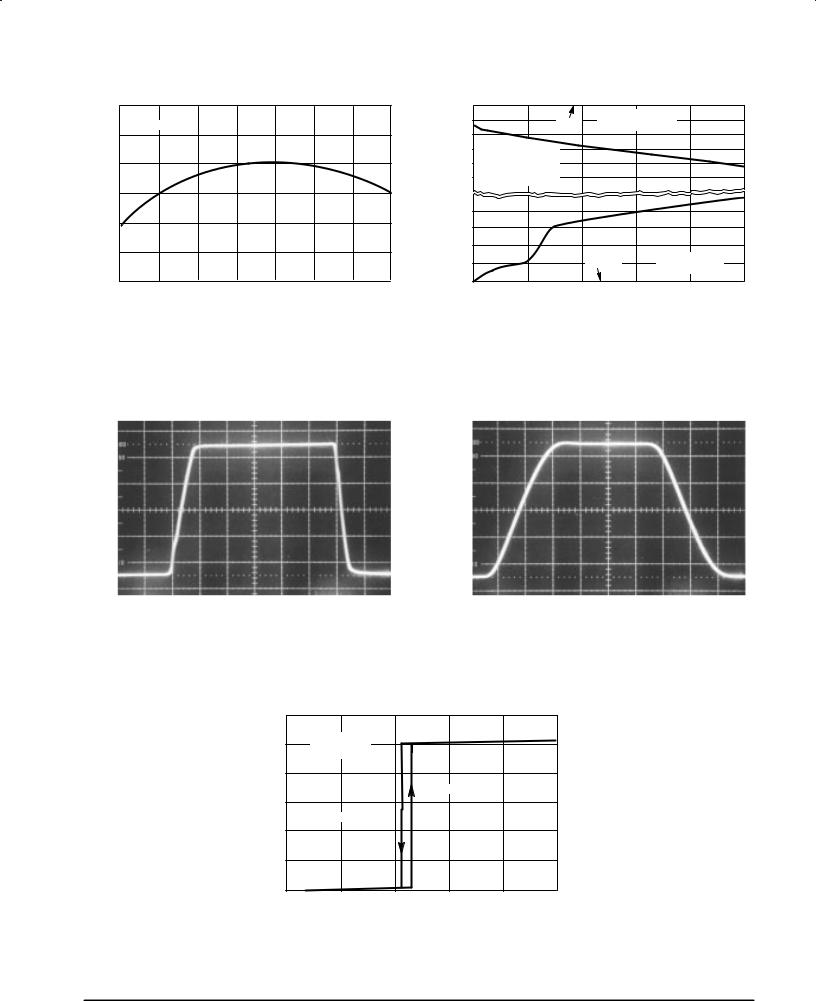
Figure 14. Output Saturation Voltage |
versus Temperature |
versus Load Current |
10 |
|
|
|
|
|
|
(V) |
0 |
|
|
Source Saturation |
|
|
|
|
|
|
|
|
|
|
80 μs Pulsed Load |
|
||||
V |
|
= 15 V |
|
|
|
|
VOLTAGE |
|
(Load to Ground) |
|
|||
9.5 |
CC |
|
|
|
|
|
|
±1.0 |
|
|
|
|
|
|
|
|
|
|
|
|
VCC = 15 V |
|
|
|
|
||
|
|
|
|
|
|
|
|
|
|
|
|
|
|
9.0 |
|
|
|
|
|
|
SATURATION |
2.0 |
120 Hz Rate |
|
|
|
|
|
|
|
|
|
|
|
|
|
|
|
|||
|
|
|
|
|
|
|
|
±2.0 |
|
|
|
|
|
8.5 |
|
|
|
|
|
|
|
|
TA = + 25°C |
|
|
|
|
|
|
|
|
|
|
|
|
|
|
|
|
|
|
8.0 |
|
|
|
|
|
|
OUTPUT, |
|
|
|
|
|
|
7.5 |
|
|
|
|
|
|
1.0 |
|
|
|
Sink Saturation |
||
|
|
|
|
|
|
|
|
|
|
|
|
|
|
|
|
|
|
|
|
|
sat |
|
|
|
Ground |
(Load to V |
) |
7.0 |
|
|
|
|
|
|
V |
0 |
|
|
|
|
CC |
|
|
|
|
|
|
|
|
|
|
|
|
||
±55 |
±25 |
0 |
25 |
50 |
75 |
100 |
125 |
0 |
0.2 |
0.4 |
0.6 |
0.8 |
1.0 |
|
|
TA, AMBIENT TEMPERATURE (°C) |
|
|
|
|
IO, OUTPUT LOAD CURRENT (A) |
|
|||||
Figure 15. Drive Output Rise and Fall Time |
Figure 16. Drive Output Rise and Fall Time |
OUTPUT RISE & FALL TIME 1.0 nF LOAD |
OUTPUT RISE & FALL TIME 10.0 nF LOAD |
50 ns/DIV |
50 ns/DIV |
Figure 17. Supply Voltage versus Supply Current
|
30 |
|
|
|
|
|
(mA) |
25 |
RT = 3.65 kΩ |
|
|
|
|
|
CT = 1.0 nF |
|
|
|
|
|
CURRENT |
20 |
|
|
|
|
|
15 |
|
|
VCC Increasing |
|
|
|
|
|
|
|
|
||
, SUPPLY |
10 |
VCC Decreasing |
|
|
|
|
|
|
|
|
|
||
|
|
|
|
|
|
|
CC |
5.0 |
|
|
|
|
|
I |
|
|
|
|
|
|
|
0 |
|
|
|
|
|
|
0 |
4.0 |
8.0 |
12 |
16 |
20 |
|
|
|
VCC, SUPPLY VOLTAGE (V) |
|
|
|
6 |
MOTOROLA ANALOG IC DEVICE DATA |
 Loading...