


MC3403D
Motorola MC3403D, MC3403DR2, MC3303P, MC3303DR2, MC3303D Datasheet
...
Order this document by MC3403/D
The MC3403 is a low cost, quad operational amplifier with true differential
inputs. The device has electrical characteristics similar to the popular
MC1741C. However, the MC3403 has several distinct advantages over
standard operational amplifier types in single supply applications. The quad
amplifier can operate at supply voltages as low as 3.0 V or as high as 36 V
with quiescent currents about one third of those associated with the
MC1741C (on a per amplifier basis). The common mode input range
includes the negative supply, thereby eliminating the necessity for external
biasing components in many applications. The output voltage range also
includes the negative power supply voltage.
• Short Circuit Protected Outputs
• Class AB Output Stage for Minimal Crossover Distortion
• True Differential Input Stage
• Single Supply Operation: 3.0 V to 36 V
• Split Supply Operation: ±1.5 V to ±18 V
• Low Input Bias Currents: 500 nA Max
• Four Amplifiers Per Package
• Internally Compensated
• Similar Performance to Popular MC1741C
• Industry Standard Pinouts
• ESD Diodes Added for Increased Ruggedness
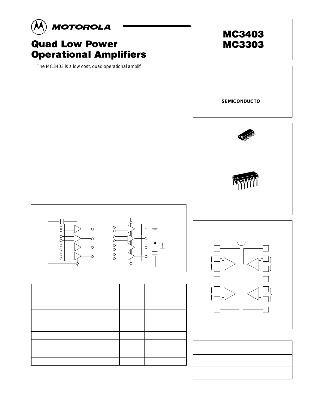
Single Supply
3.0 V to 36 V
V
CC
1
2
Split Supplies
V
CC
1
2
1.5 V to 18 V
QUAD DIFFERENTIAL INPUT
OPERATIONAL AMPLIFIERS
SEMICONDUCTOR
TECHNICAL DATA
14
1
D SUFFIX
PLASTIC PACKAGE
CASE 751A
(SO–14)
14
1
P SUFFIX
PLASTIC PACKAGE
CASE 646
PIN CONNECTIONS
3
4
VEE, Gnd
3
4
V
EE
1.5 V to 18 V
MAXIMUM RATINGS
Rating Symbol Value Unit
Power Supply Voltages Vdc
Single Supply V
Split Supplies VCC, V
Input Differential V oltage Range (Note 1) V
Input Common Mode Voltage Range
(Notes 1, 2)
Storage Temperature Range T
Operating Ambient Temperature Range T
MC3303 –40 to +85
MC3403 0 to +70
Junction Temperature T
NOTES: 1. Split power supplies.
2.For supply voltages less than ±18 V, the absolute maximum input voltage is equal
to the supply voltage.
V
CC
EE
IDR
ICR
stg
A
J
36
±18
±36 Vdc
±18 Vdc
–55 to +125 °C
150 °C
MOTOROLA ANALOG IC DEVICE DATA
°C
Out 1
Inputs 1
V
CC
Inputs 2
Out 2
1
2
–
1
+
3
4
5
+
2
–
6
78
(Top View)
14
Out 4
13
–
3
+
+
4
–
Inputs 4
12
11
VEE/Gnd
10
Inputs 3
9
Out 3
ORDERING INFORMATION
Operating
Device
MC3303D
MC3303P
MC3403D
MC3403P
Motorola, Inc. 1996 Rev 5
Temperature Range
TA = – 40° to +85°C
TA = 0° to +70°C
Package
SO–14
Plastic DIP
SO–14
Plastic DIP
1
MC3403 MC3303
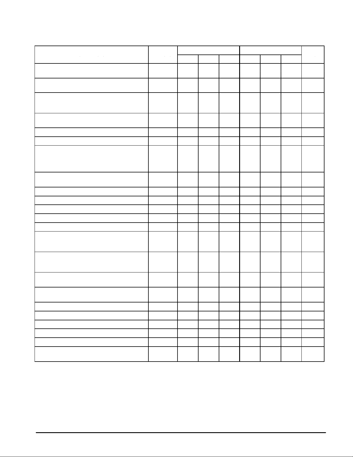
ELECTRICAL CHARACTERISTICS
TA = 25°C, unless otherwise noted.)
Characteristic Symbol
Input Offset Voltage V
TA = T
Input Offset Current I
TA = T
Large Signal Open Loop Voltage Gain A
VO = ±10 V, RL = 2.0 kΩ 20 200 – 20 200 –
TA = T
Input Bias Current I
TA = T
Output Impedance f = 20 Hz z
Input Impedance f = 20 Hz z
Output Voltage Range V
RL = 10 kΩ ±12 ±13.5 – 12 12.5 –
RL = 2.0 kΩ ±10 ±13 – 10 12 –
RL = 2.0 kΩ, TA = T
Input Common Mode Voltage Range V
Common Mode Rejection RS ≤ 10 k Ω CMR 70 90 – 70 90 – dB
Power Supply Current (VO = 0) RL = ∞ ICC, I
Individual Output Short–Circuit Current (Note 2) I
Positive Power Supply Rejection Ratio PSRR+ – 30 150 – 30 150 µV/V
Negative Power Supply Rejection Ratio PSRR– – 30 150 – 30 150 µV/V
Average Temperature Coefficient of Input
Offset Current
TA = T
Average Temperature Coefficient of Input
Offset Voltage
TA = T
Power Bandwidth
AV = 1, RL = 10 kΩ, VO = 20 V(p–p), THD = 5%
Small–Signal Bandwidth
AV = 1, RL = 10 kΩ, VO = 50 mV
Slew Rate AV = 1, Vi = –10 V to +10 V SR – 0.6 – – 0.6 – V/µs
Rise Time AV = 1, RL = 10 kΩ, VO = 50 mV t
Fall Time AV = 1, RL = 10 kΩ, VO = 50 mV t
Overshoot AV = 1, RL = 10 kΩ, VO = 50 mV os – 20 – – 20 – %
Phase Margin AV = 1, RL = 2.0 kΩ, VO = 200 pF φm – 60 – – 60 – Degrees
Crossover Distortion
(Vin = 30 mVpp,V
NOTES: 1. T
to T
high
high
high
high
high
high
high
T
= 0°C for MC3403, –40°C for MC3303
low
2.Not to exceed maximum package power dissipation.
(Note 1) – – 12 – – 10
low
to T
low
to T
low
to T
low
to T
high
to T
low
to T
low
= 2.0 Vpp, f = 10 kHz)
out
= +70°C for MC3403, +85°C for MC3303
low
(VCC = +15 V, VEE = –15 V for MC3403; VCC = +14 V, VEE = Gnd for MC3303
MC3403 MC3303
Min Typ Max Min Typ Max
IO
IO
VOL
IB
o
i
O
ICR
EE
SC
∆IIO/∆T – 50 – – 50 – pA/°C
∆VIO/∆T – 10 – – 10 – µV/°C
BWp – 9.0 – – 9.0 – kHz
BW – 1.0 – – 1.0 – MHz
TLH
TLH
– – 1.0 – – 1.0 – %
– 2.0 10 – 2.0 8.0 mV
– 30 50 – 30 75 nA
– – 200 – – 250
15 – – 15 – –
– –200 –500 – –200 –500 nA
– – –800 – – –1000
– 75 – – 75 – Ω
0.3 1.0 – 0.3 1.0 – MΩ
±10 – – 10 – –
+13 V
–V
±10 ±20 ±45 ±10 ±30 ±45 mA
+13 V
–V
EE
– 2.8 7.0 – 2.8 7.0 mA
– 0.35 – – 0.35 – µs
– 0.35 – – 0.35 – µs
EE
– +12 V
–V
EE
+12.5 V
–V
EE
Unit
V/mV
V
– V
2
MOTOROLA ANALOG IC DEVICE DATA
MC3403 MC3303
ELECTRICAL CHARACTERISTICS (V
Characteristic Symbol
Input Offset Voltage V
Input Offset Current I
Input Bias Current I
Large Signal Open Loop Voltage Gain
RL = 2.0 kΩ
Power Supply Rejection Ratio PSRR – – 150 – – 150 µV/V
Output Voltage Range (Note 3) V
RL = 10 kΩ, VCC = 5.0 V 3.3 3.5 – 3.3 3.5 –
RL = 10 kΩ, 5.0 ≤ VCC ≤ 30 V VCC–2.0 VCC–1.7 – VCC–2.0 VCC–1.7 –
Power Supply Current I
Channel Separation
f = 1.0 kHz to 20 kHz
(Input Referenced)
NOTES: 3. Output will swing to ground with a 10 kΩ pull down resistor.
= 5.0 V, VEE = Gnd, TA = 25°C, unless otherwise noted.)
CC
MC3403 MC3303
Min Typ Max Min Typ Max
IO
IO
IB
A
VOL
OR
CC
CS – –120 – – –120 – dB
– 2.0 10 – – 10 mV
– 30 50 – – 75 nA
– –200 –500 – – –500 nA
10 200 – 10 200 – V/mV
– 2.5 7.0 – 2.5 7.0 mA
Unit
Vpp
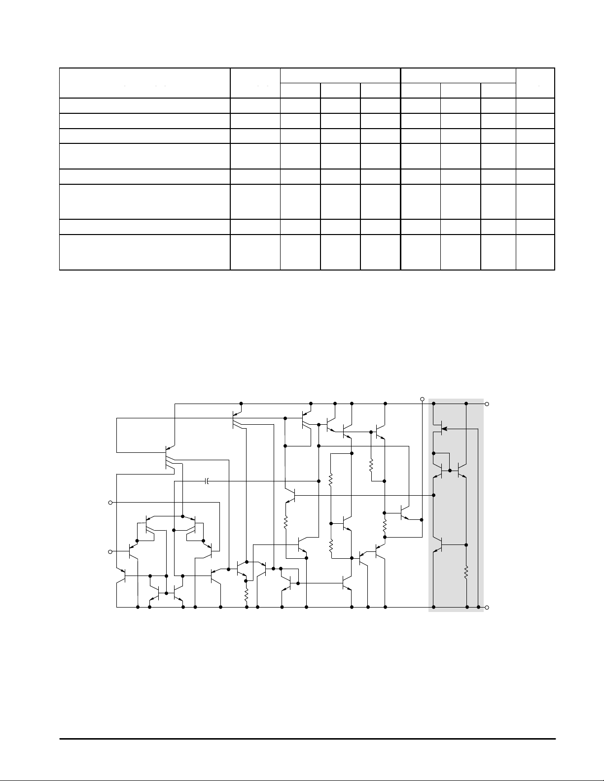
Inputs
Representative Schematic Diagram
(1/4 of Circuit Shown)
Output
Q18Q19
Q20
Q23
5.0 pF
Q7
Q1
2.0 k
Q9
37 k
Q10
Q8
+
Q22
–
Q21
Q2
Q3 Q4
Q24
Q25
Q6
Q5
60 k
31k
Q17
40 k
Q13
Q11
Q16
Q15
25
Q12
Bias Circuitry
Common to Four
Amplifiers
Q27
Q29
Q28
Q30
2.4 k
V
CC
VEE (Gnd)
MOTOROLA ANALOG IC DEVICE DATA
3
 Loading...