


MC33461SQ-43CTR
MOTOROLA MC33461SQ-43CTR, MC33461SQ-45CTR, MC33461SQ-27CTR, MC33461SQ-28CTR, MC33461SQ-30CTR Datasheet
...
Semiconductor Components Industries, LLC, 1999
November, 1999 – Rev. 2
1 Publication Order Number:
MC33460/D
MC33460, MC33461
Under Voltage Detector
Series
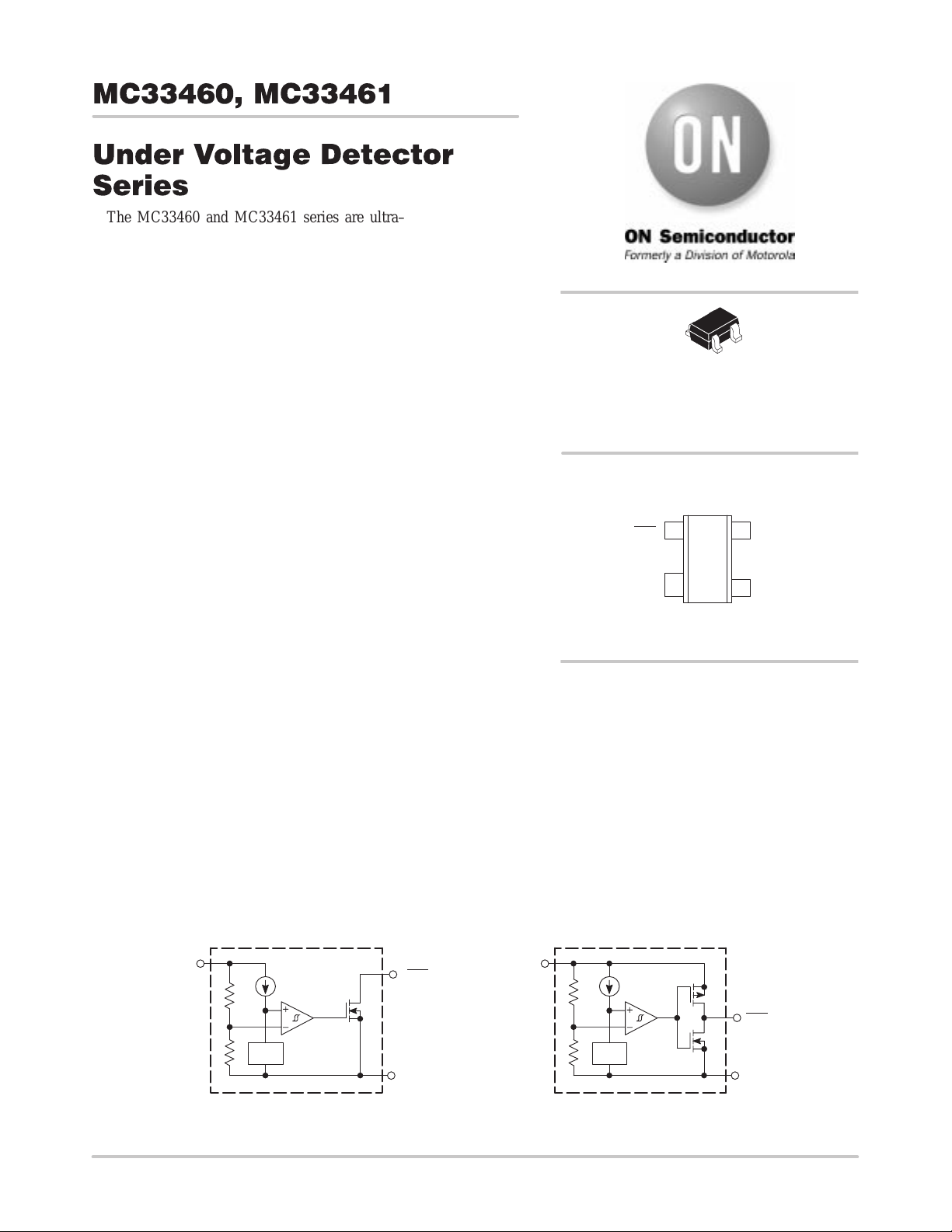
The MC33460 and MC33461 series are ultra–low power CMOS
under–voltage detectors with very tight threshold accuracy
specifically designed for accurate monitoring of power supplies. The
devices are optimized for use in battery powered systems where low
quiescent current and small packaging are required. The device
generates an active–low signal whenever the input voltage falls below
the factory set ±2% threshold. Hysteresis is provided to ensure reliable
output switching.
The MC33460/1 series features a highly accurate voltage reference,
a comparator with a precision voltage threshold, and built–in
hysteresis to prevent erratic operation and a choice of output
configurations between Open Drain (MC33460) and complementary
push–pull (MC33461). The products are offered in 9 standard voltage
thresholds ranging from 0.9V to 4.5V. Other threshold voltages from
1.0 to 5.0V are available in 100mV steps. The devices can operate to a
very low input voltage level and are housed in the ultra–miniature
SC–82AB package.
Features
• Available in Open Drain or Push–Pull Output
• Output State Guaranteed to V
in
= 0.8 V
• Tight Detector Voltage Accuracy (±2.0%)
• Extended T emperature Operation (–40°C to 85°C)
• Ultra Low Quiescent Current (0.8 µA at V
in
= 1.5 V typical)
• Wide Range of Operating Voltage (0.7 V to 10 V)
Applications
• Low Battery Detector
• Power–Fail Indicator
• Microprocessor Reset Generator
• Window Comparator
• Battery Backup Circuit
Representative Block Diagrams
MC33460
Nch Open Drain Configuration
MC33461
CMOS Configuration
V
ref
V
in
OUT
GND
V
ref
V
in
OUT
GND
SC–82AB
SQ SUFFIX
CASE 419C
http://onsemi.com
See detailed ordering and shipping information in the package
dimensions section on page 2 of this data sheet.
ORDERING INFORMATION
PIN CONNECTIONS
4
1
14
3
2
(Top View)
V
in
OUT
GND
N/C
MC33460, MC33461
http://onsemi.com
2
ORDERING INFORMATION
Device
Threshold
Voltage
Type Marking
Package
(Qty/Reel)
MC33460SQ–09ATR 0.9
K9
MC33460SQ–20ATR 2.0 M0
MC33460SQ–27ATR 2.7
M7
MC33460SQ–28ATR 2.8
Nch
p
M8
MC33460SQ–30ATR 3.0
Oen
N0
MC33460SQ–32ATR 3.2
Drain
N2
MC33460SQ–43ATR 4.3 P3
MC33460SQ–45ATR 4.5 P5
3000
U
n
it
s
MC33461SQ–09CTR 0.9
T9
on
7
i
nc
h
Reel
MC33461SQ–20CTR 2.0 V0
Reel
MC33461SQ–27CTR 2.7 V7
MC33461SQ–28CTR 2.8
V8
MC33461SQ–30CTR 3.0
CMOS
W0
MC33461SQ–32CTR 3.2 W2
MC33461SQ–43CTR 4.3 X3
MC33461SQ–45CTR 4.5 X5
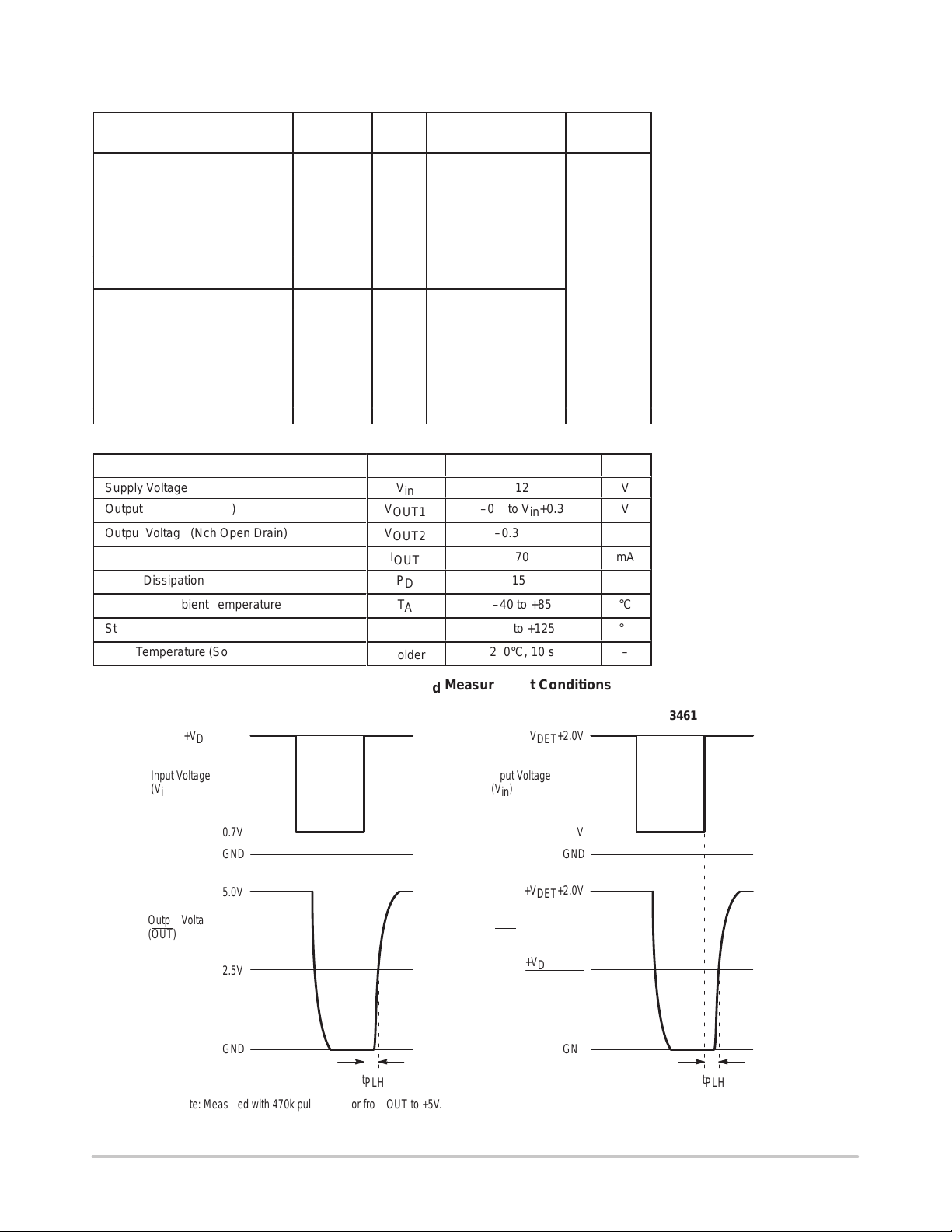
MAXIMUM RATINGS
Rating Symbol Value Unit
Supply Voltage
V
in
12
V
Output Voltage (CMOS)
V
OUT1
–0.3 to V
in
+0.3
V
Output Voltage (Nch Open Drain)
V
OUT2
–0.3 to 12
V
Output Current
I
OUT
70
mA
Power Dissipation
P
D
150
mW
Operating Ambient Temperature
T
A
–40 to +85
°C
Storage Temperature Range
T
stg
–40 to +125
°C
Lead Temperature (Soldering)
T
solder
260°C, 10 s
–
Input Voltage
(V
in
)
Figure 1. T
pd
Measurement Conditions
Output Voltage
(OUT
)
0.7V
GND
5.0V
2.5V
GND
+V
DET
+2.0V
MC33460 MC33461
t
PLH
Input Voltage
(V
in
)
0.7V
GND
GND
+V
DET
+2.0V
t
PLH
+V
DET
+2.0V
+V
DET
+2.0V
2
Output Voltage
(OUT
)
Note: Measured with 470k pullup resistor from OUT
to +5V.
MC33460, MC33461
http://onsemi.com
3
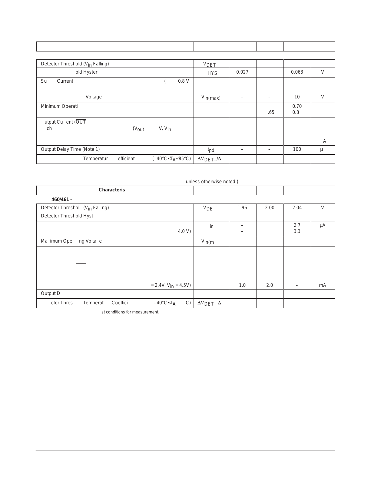
ELECTRICAL CHARACTERISTICS (For all values T
A
= 25°C, unless otherwise noted.)
Characteristic
Symbol Min Typ Max Unit
MC33460/461 – 0.9
Detector Threshold (V
in
Falling)
V
DET–
0.882
0.900
0.918
V
Detector Threshold Hysteresis V
HYS
0.027 0.045 0.063 V
Supply Current (V
in
= 0.8 V)
(V
in
= 2.9 V)
I
in
–
–
0.8
1.0
2.4
3.0
µA
Maximum Operating Voltage V
in(max)
– – 10 V
Minimum Operating Voltage
(–40°C≤T
A
≤85°C)
V
in(min)
–
–
0.55
0.65
0.70
0.80
V
Output Current (OUT)
I
OUT
Nch (V
out
= 0.05V, V
in
= 0.70V) 0.01 0.05 – mA
(V
out
= 0.50V, V
in
= 0.85V) 0.05 0.50 – mA
CMOS Output High (V
out
= 2.4V, V
in
= 4.5V) 1.0 2.0 – mA
Output Delay Time (Note 1)
t
pd
–
–
100
µs
Detector Threshold Temperature Coefficient (–40°C≤T
A
≤85°C)
D
V
DET–
/
D
T
–
±100
–
PPM/°C
NOTES: 1.Refer to Figure 1 for test conditions for measurement.
ELECTRICAL CHARACTERISTICS (For all values T
A
= 25°C, unless otherwise noted.)
Characteristic
Symbol Min Typ Max Unit
MC33460/461 – 2.0
Detector Threshold (V
in
Falling)
V
DET–
1.96
2.00
2.04
V
Detector Threshold Hysteresis V
HYS
0.06 0.10 0.14 V
ББББББББББББББББ
Á
Supply Current (V
in
= 1.9 V)
(V
in
= 4.0 V)
ÁÁÁ
Á
I
in
ÁÁ
Á
–
–
ÁÁ
Á
0.9
1.1
ÁÁ
Á
2.7
3.3
Á
Á
µA
Maximum Operating Voltage V
in(max)
– – 10 V
Minimum Operating Voltage
(–40°C≤T
A
≤85°C)
V
in(min)
–
–
0.55
0.65
0.70
0.80
V
Output Current (OUT)
I
OUT
Nch (V
out
= 0.05V, V
in
= 0.70V) 0.01 0.05 – mA
(V
out
= 0.50V, V
in
= 1.5V) 1.0 2.0 – mA
CMOS Output High (V
out
= 2.4V, V
in
= 4.5V) 1.0 2.0 – mA
Output Delay Time (Note 1)
t
pd
–
–
100
µs
Detector Threshold Temperature Coefficient (–40°C≤T
A
≤85°C)
D
V
DET–
/
D
T
–
±100
–
PPM/°C
NOTES: 1.Refer to Figure 1 for test conditions for measurement.
MC33460, MC33461
http://onsemi.com
4
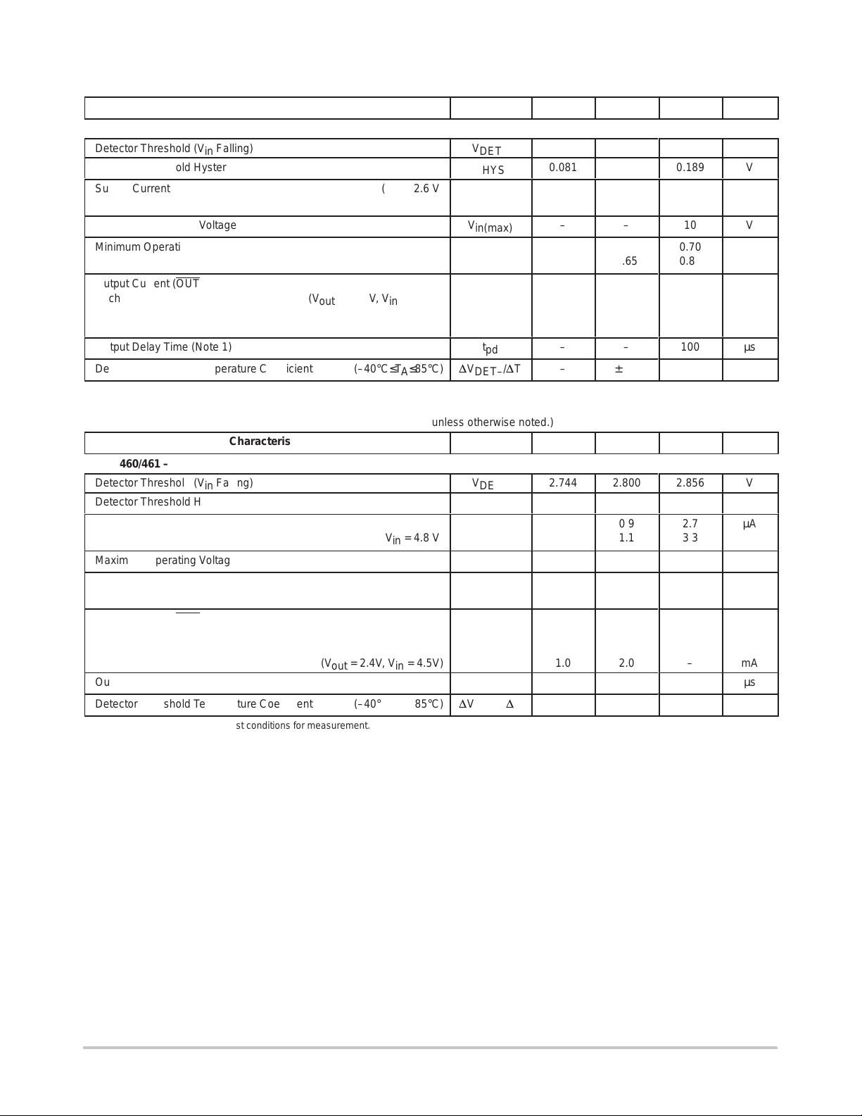
ELECTRICAL CHARACTERISTICS (For all values T
A
= 25°C, unless otherwise noted.)
Characteristic
Symbol Min Typ Max Unit
MC33460/461 – 2.7
Detector Threshold (V
in
Falling)
V
DET–
2.646
2.700
2.754
V
Detector Threshold Hysteresis V
HYS
0.081 0.135 0.189 V
Supply Current (V
in
= 2.6 V)
(V
in
= 4.7 V)
I
in
–
–
0.9
1.1
2.7
3.3
µA
Maximum Operating Voltage V
in(max)
– – 10 V
Minimum Operating Voltage
(–40°C≤T
A
≤85°C)
V
in(min)
–
–
0.55
0.65
0.70
0.80
V
Output Current (OUT)
I
OUT
Nch (V
out
= 0.05V, V
in
= 0.70V) 0.01 0.05 – mA
(V
out
= 0.50V, V
in
= 1.5V) 1.0 2.0 – mA
CMOS Output High (V
out
= 2.4V, V
in
= 4.5V) 1.0 2.0 – mA
Output Delay Time (Note 1)
t
pd
–
–
100
µs
Detector Threshold Temperature Coefficient (–40°C≤T
A
≤85°C)
D
V
DET–
/
D
T
–
±100
–
PPM/°C
NOTES: 1.Refer to Figure 1 for test conditions for measurement.
ELECTRICAL CHARACTERISTICS (For all values T
A
= 25°C, unless otherwise noted.)
Characteristic
Symbol Min Typ Max Unit
MC33460/461 – 2.8
Detector Threshold (V
in
Falling)
V
DET–
2.744
2.800
2.856
V
Detector Threshold Hysteresis V
HYS
0.084 0.140 0.196 V
ББББББББББББББББ
Á
Supply Current (V
in
= 2.7 V)
(V
in
= 4.8 V)
ÁÁÁ
Á
I
in
ÁÁ
Á
–
–
ÁÁ
Á
0.9
1.1
ÁÁ
Á
2.7
3.3
Á
Á
µA
Maximum Operating Voltage V
in(max)
– – 10 V
Minimum Operating Voltage
(–40°C≤T
A
≤85°C)
V
in(min)
–
–
0.55
0.65
0.70
0.80
V
Output Current (OUT)
I
OUT
Nch (V
out
= 0.05V, V
in
= 0.70V) 0.01 0.05 – mA
(V
out
= 0.50V, V
in
= 1.5V) 1.0 2.0 – mA
CMOS Output High (V
out
= 2.4V, V
in
= 4.5V) 1.0 2.0 – mA
Output Delay Time (Note 1)
t
pd
–
–
100
µs
Detector Threshold Temperature Coefficient (–40°C≤T
A
≤85°C)
D
V
DET–
/
D
T
–
±100
–
PPM/°C
NOTES: 1.Refer to Figure 1 for test conditions for measurement.
 Loading...