


MC33204VD
Motorola MC33204VD, MC33204VDTB, MC33204P, MC33201D, MC33201P Datasheet
...
LOW VOLTAGE
RAIL–TO–RAIL
OPERATIONAL AMPLIFIERS
Order this document by MC33201/D
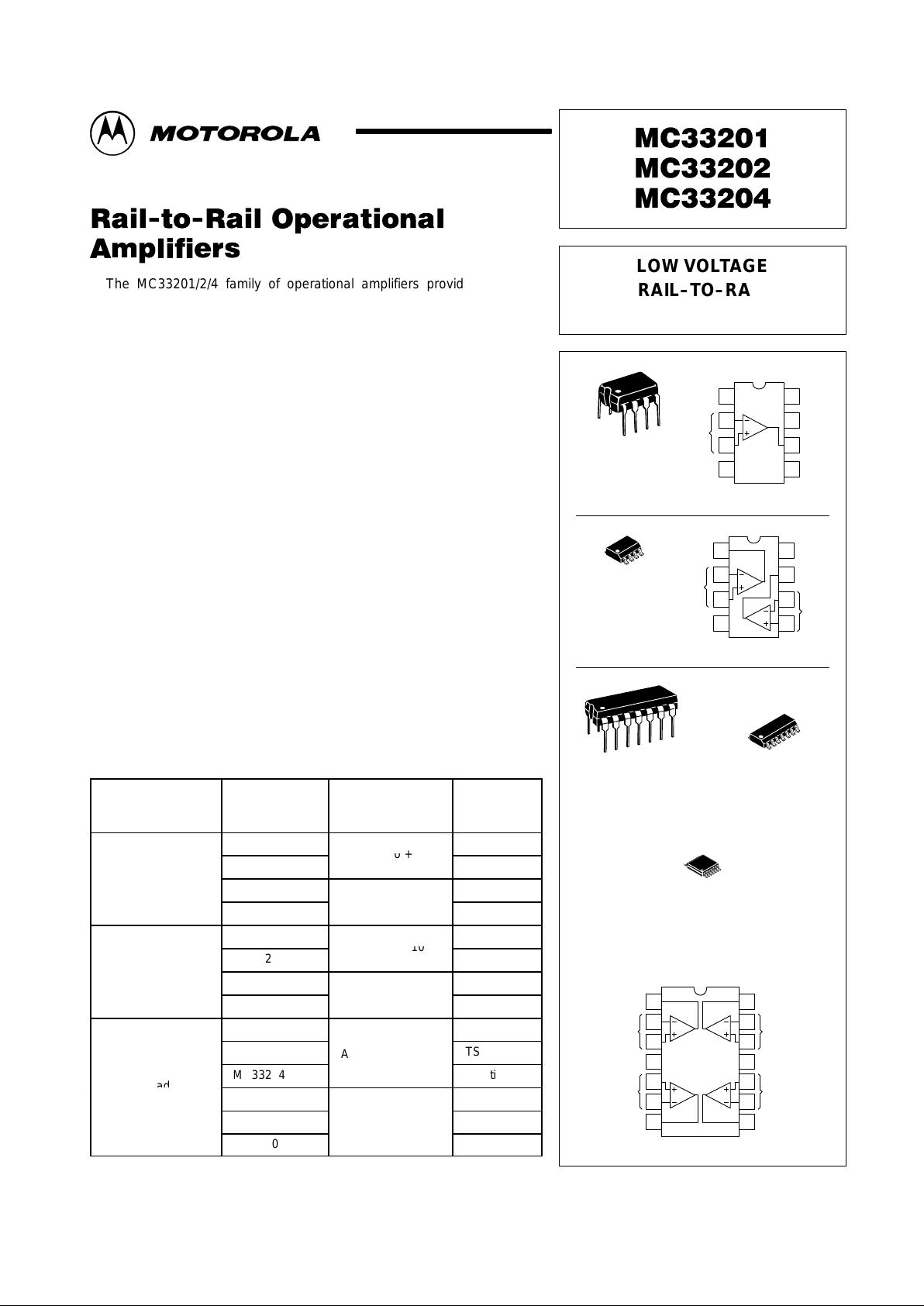
P SUFFIX
PLASTIC PACKAGE
CASE 626
(Quad, Top View)
8
1
D SUFFIX
PLASTIC PACKAGE
CASE 751
(SO–8)
8
1
P SUFFIX
PLASTIC PACKAGE
CASE 646
14
1
D SUFFIX
PLASTIC PACKAGE
CASE 751A
(SO–14)
14
1
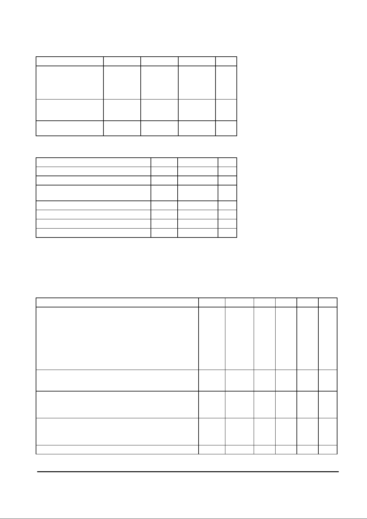
Output 1
Inputs 1
V
EE
V
CC
Output 2
Inputs 2
1
2
6
7
8
5
3
2
1
4
Output 1
Inputs 1
V
CC
Output 4
Inputs 4
1
12
13
14
11
3
2
1
4
105
96
Output 2
8
7
Inputs 2
2
4
3
V
EE
Inputs 3
Output 3
(Dual, Top View)
6
7
8
5
3
2
1
4
NC
Inputs
V
EE
NC
V
CC
NC
Output
(Single, Top View)
DTB SUFFIX
PLASTIC PACKAGE
CASE 948G
(TSSOP–14)
14
1
1
MOTOROLA ANALOG IC DEVICE DATA
The MC33201/2/4 family of operational amplifiers provide rail–to–rail
operation on both the input and output. The inputs can be driven as high as
200 mV beyond the supply rails without phase reversal on the outputs, and
the output can swing within 50 mV of each rail. This rail–to–rail operation
enables the user to make full use of the supply voltage range available. It is
designed to work at very low supply voltages (± 0.9 V) yet can operate with a
supply of up to +12 V and ground. Output current boosting techniques
provide a high output current capability while keeping the drain current of the
amplifier to a minimum. Also, the combination of low noise and distortion with
a high slew rate and drive capability make this an ideal amplifier for audio
applications.
• Low Voltage, Single Supply Operation
(+1.8 V and Ground to +12 V and Ground)
• Input Voltage Range Includes both Supply Rails
• Output Voltage Swings within 50 mV of both Rails
• No Phase Reversal on the Output for Over–driven Input Signals
• High Output Current (I
SC
= 80 mA, Typ)
• Low Supply Current (I
D
= 0.9 mA, Typ)
• 600 Ω Output Drive Capability
• Extended Operating Temperature Ranges
(–40° to +105°C and –55° to +125°C)
• Typical Gain Bandwidth Product = 2.2 MHz
• Offered in New TSSOP Package Including Standard SOIC and
DIP Packages
ORDERING INFORMATION
Operational
Amplifier Function
Device
Operating
Temperature
Range
Package
MC33201D
–
°
°
SO–8
MC33201P
T
A
= –40 ° to +
105°C
Plastic DIP
Single
MC33201VD
TA = –55 ° to
SO–8
MC33201VP
A
+125°C
Plastic DIP
MC33202D
–
°
°
SO–8
MC33202P
T
A
= –
40 ° to +105°C
Plastic DIP
Dual
MC33202VD
TA = –55 ° to
SO–8
MC33202VP
A
+125°C
Plastic DIP
MC33204D
SO–14
MC33204DTB
TA= –40 ° to +105°C
TSSOP–14
MC33204P Plastic DIP
Quad
MC33204VD
SO–14
MC33204VDTB
TA = –55 ° to
+125°C
TSSOP–14
MC33204VP
+125 C
Plastic DIP
Motorola, Inc. 1996 Rev 2
MC33201 MC33202 MC33204
2
MOTOROLA ANALOG IC DEVICE DATA
DC ELECTRICAL CHARACTERISTICS (T
A
= 25°C)
Characteristic VCC = 2.0 V VCC = 3.3 V VCC = 5.0 V Unit
Input Offset Voltage
VIO
(max)
MC33201
MC33202
MC33204
± 8.0
±10
±12
± 8.0
±10
±12
± 6.0
± 8.0
±10
mV
Output Voltage Swing
VOH (RL = 10 kΩ)
VOL (RL = 10 kΩ)
1.9
0.10
3.15
0.15
4.85
0.15
V
min
V
max
Power Supply Current
per Amplifier (ID)
1.125 1.125 1.125
mA
Specifications at VCC = 3.3 V are guaranteed by the 2.0 V and 5.0 V tests. VEE = Gnd.
MAXIMUM RATINGS
Rating Symbol Value Unit
Supply Voltage (VCC to VEE) V
S
+13 V
Input Differential Voltage Range V
IDR
(Note 1) V
Common Mode Input Voltage Range (Note 2) V
CM
VCC + 0.5 V to
VEE – 0.5 V
V
Output Short Circuit Duration t
s
(Note 3) sec
Maximum Junction Temperature T
J
+150 °C
Storage Temperature T
stg
– 65 to +150 °C
Maximum Power Dissipation P
D
(Note 3) mW
NOTES: 1.The differential input voltage of each amplifier is limited by two internal parallel back–to–back
diodes. For additional differential input voltage range, use current limiting resistors in series
with the input pins.
2.The input common mode voltage range is limited by internal diodes connected from the inputs
to both supply rails. Therefore, the voltage on either input must not exceed either supply rail by
more than 500 mV.
3.Power dissipation must be considered to ensure maximum junction temperature (TJ) is not
exceeded. (See Figure 2)
DC ELECTRICAL CHARACTERISTICS (V
CC
= + 5.0 V, VEE = Ground, TA = 25°C, unless otherwise noted.)
Characteristic
Figure Symbol Min Typ Max Unit
Input Offset Voltage (VCM 0 V to 0.5 V, VCM 1.0 V to 5.0 V)
MC33201: TA = + 25°C
MC33201: TA = – 40° to +105°C
MC33201: TA = – 55° to +125°C
MC33202: TA = + 25°C
MC33202: TA = – 40° to +105°C
MC33202: TA = – 55° to +125°C
MC33204: TA = + 25°C
MC33204: TA = – 40° to +105°C
MC33204: TA = – 55° to +125°C
3 VIO
–
–
–
–
–
–
–
–
–
–
–
–
–
–
–
–
–
–
6.0
9.0
13
8.0
11
14
10
13
17
mV
Input Offset Voltage Temperature Coefficient (RS = 50 Ω)
TA = – 40° to +105°C
TA = – 55° to +125°C
4 ∆VIO/∆T
–
–
2.0
2.0
–
–
µV/°C
Input Bias Current (VCM = 0 V to 0.5 V, VCM = 1.0 V to 5.0 V)
TA = + 25°C
TA = – 40° to +105°C
TA = – 55° to +125°C
5, 6 IIB
–
–
–
80
100
–
200
250
500
nA
Input Offset Current (VCM = 0 V to 0.5 V, VCM = 1.0 V to 5.0 V)
TA = + 25°C
TA = – 40° to +105°C
TA = – 55° to +125°C
– IIO
–
–
–
5.0
10
–
50
100
200
nA
Common Mode Input Voltage Range – V
ICR
V
EE
– V
CC
V
MC33201 MC33202 MC33204
3
MOTOROLA ANALOG IC DEVICE DATA
DC ELECTRICAL CHARACTERISTICS (continued) (V
CC
= + 5.0 V, VEE = Ground, TA = 25°C, unless otherwise noted.)
Characteristic UnitMaxTypMinSymbolFigure
Large Signal Voltage Gain (VCC = + 5.0 V, VEE = – 5.0 V)
RL = 10 kΩ
RL = 600 Ω
7 A
VOL
50
25
300
250
–
–
kV/V
Output Voltage Swing (VID = ± 0.2 V)
RL = 10 kΩ
RL = 10 kΩ
RL = 600 Ω
RL = 600 Ω
8, 9, 10
V
OH
V
OL
V
OH
V
OL
4.85
–
4.75
–
4.95
0.05
4.85
0.15
–
0.15
–
0.25
V
Common Mode Rejection (Vin = 0 V to 5.0 V) 11 CMR 60 90 – dB
Power Supply Rejection Ratio
VCC/VEE = 5.0 V/Gnd to 3.0 V/Gnd
12 PSRR
500 25 –
µV/V
Output Short Circuit Current (Source and Sink) 13, 14 I
SC
50 80 – mA
Power Supply Current per Amplifier (VO = 0 V)
TA = – 40° to +105°C
TA = – 55° to +125°C
15 I
D
–
–
0.9
0.9
1.125
1.125
mA
AC ELECTRICAL CHARACTERISTICS (V
CC
= + 5.0 V, VEE = Ground, TA = 25°C, unless otherwise noted.)
Characteristic Figure Symbol Min Typ Max Unit
Slew Rate
(VS = ± 2.5 V, VO = – 2.0 V to + 2.0 V, RL = 2.0 kΩ, AV = +1.0)
16, 26 SR
0.5 1.0 –
V/µs
Gain Bandwidth Product (f = 100 kHz) 17 GBW – 2.2 – MHz
Gain Margin (RL = 600 Ω, CL = 0 pF) 20, 21, 22 A
M
– 12 – dB
Phase Margin (RL = 600 Ω, CL = 0 pF) 20, 21, 22
O
M
– 65 – Deg
Channel Separation (f = 1.0 Hz to 20 kHz, AV = 100) 23 CS – 90 – dB
Power Bandwidth (VO = 4.0 Vpp, RL = 600 Ω, THD ≤ 1 %) BW
P
– 28 – kHz
Total Harmonic Distortion (RL = 600 Ω, VO = 1.0 Vpp, AV = 1.0)
f = 1.0 kHz
f = 10 kHz
24 THD
–
–
0.002
0.008
–
–
%
Open Loop Output Impedance
(VO = 0 V, f = 2.0 MHz, AV = 10)
ZO
– 100 –
Ω
Differential Input Resistance (VCM = 0 V) R
in
– 200 – kΩ
Differential Input Capacitance (VCM = 0 V) C
in
– 8.0 – pF
Equivalent Input Noise Voltage (RS = 100 Ω)
f = 10 Hz
f = 1.0 kHz
25 e
n
–
–
25
20
–
–
Hz
nV/
Equivalent Input Noise Current
f = 10 Hz
f = 1.0 kHz
25 i
n
–
–
0.8
0.2
–
–
pA/
Hz
MC33201 MC33202 MC33204
4
MOTOROLA ANALOG IC DEVICE DATA
V
in –
V
out
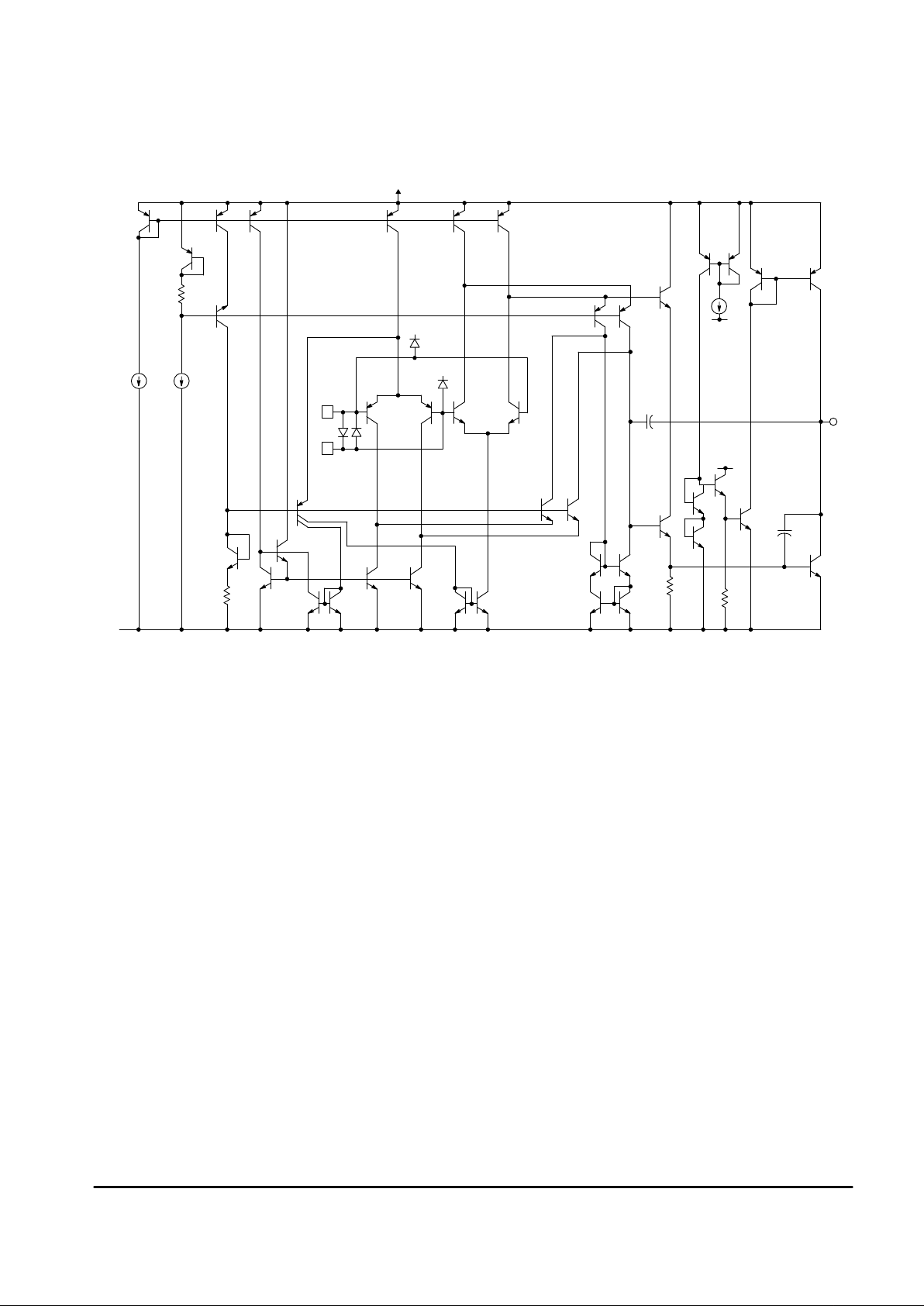
Figure 1. Circuit Schematic
(Each Amplifier)
V
EE
V
CC
V
CC
V
CC
V
CC
V
in +
V
EE
This device contains 70 active transistors (each amplifier).
 Loading...