


Motorola MC34063AMEL, MC34063AML1, MC34063AML2, MC34063AP1, MC34063AD Datasheet
...Order this document by MC34063A/D
DC-to-DC Converter
Control Circuits
The MC34063A Series is a monolithic control circuit containing the primary functions required for DC±to±DC converters. These devices consist of an internal temperature compensated reference, comparator, controlled duty cycle oscillator with an active current limit circuit, driver and high current output switch. This series was specifically designed to be incorporated in Step±Down and Step±Up and Voltage±Inverting applications with a minimum number of external components. Refer to Application Notes AN920A/D and AN954/D for additional design information.
•Operation from 3.0 V to 40 V Input
•Low Standby Current
•Current Limiting
•Output Switch Current to 1.5 A
•Output Voltage Adjustable
•Frequency Operation to 100 kHz
•Precision 2% Reference
Representative Schematic Diagram
Drive 8 |
|
|
1 Switch |
|
Collector |
|
|
|
Collector |
|
|
S Q |
Q2 |
|
|
|
R |
|
Q1 |
|
7 |
|
|
|
Ipk |
|
100 |
2 Switch |
|
|
|
|||
Sense |
|
|
|
|
|
Ipk |
|
|
Emitter |
|
CT |
|
|
|
|
Oscillator |
|
|
|
VCC |
6 |
|
|
3 Timing |
|
Comparator |
1.25 V |
Capacitor |
|
|
+ |
|
|
|
|
|
|
Reference |
|
±Regulator
Comparator 5 |
4 |
Inverting |
Gnd |
Input |
(Bottom View) |
|
This device contains 51 active transistors.
MC34063A
MC33063A
DC±to±DC CONVERTER
CONTROL CIRCUITS
SEMICONDUCTOR
TECHNICAL DATA
8
1
P, P1 SUFFIX
PLASTIC PACKAGE
CASE 626
8
1
D SUFFIX
PLASTIC PACKAGE
CASE 751
(SO±8)
PIN CONNECTIONS
Switch |
|
|
|
|
|
|
Driver |
1 |
|
|
|
|
8 |
||
Collector |
|
|
|
|
Collector |
||
|
|
|
|
|
|
||
Switch |
|
|
|
|
|
|
|
2 |
|
|
|
|
7 |
Ipk Sense |
|
Emitter |
|
|
|
|
|||
Timing |
|
|
|
|
|
|
|
3 |
|
|
|
|
6 |
VCC |
|
Capacitor |
|
|
|
|
|
|
Comparator |
|
|
|
|
|
|
||
|
|
|
|
|
|
|
|
Gnd |
4 |
|
|
|
|
5 |
|
|
|
|
|
Inverting |
|||
|
|
|
|
|
|
|
Input |
|
|
|
|
|
|
|
|
|
|
|
(Top View) |
||||
|
|
|
|
||||
ORDERING INFORMATION
|
Operating |
|
|
Device |
Temperature Range |
Package |
|
|
|
|
|
MC33063AD |
TA = ± 40° to +85°C |
SO±8 |
|
|
|
||
MC33063AP1 |
Plastic DIP |
||
|
|||
|
|
|
|
MC33063AVD |
TA = ±40° to +125°C |
SO±8 |
|
|
|
||
MC33063AVP |
Plastic DIP |
||
|
|||
|
|
|
|
MC34063AD |
TA = 0° to +70°C |
SO±8 |
|
|
|
||
MC34063AP1 |
Plastic DIP |
||
|
|||
|
|
|
Motorola, Inc. 1996 |
Rev 5 |

MC34063A MC33063A
MAXIMUM RATINGS
Rating |
|
Symbol |
Value |
Unit |
|
|
|
|
|
|
|
||
|
|
|
|
|
|
|
|
|
|
|
|
|
|
Power Supply Voltage |
|
VCC |
|
40 |
|
Vdc |
|
|
|
|
|
|
|
Comparator Input Voltage Range |
|
VIR |
|
± 0.3 to + 40 |
Vdc |
|
|
|
|
|
|
|
|
Switch Collector Voltage |
|
VC(switch) |
40 |
|
Vdc |
|
|
|
|
|
|
|
|
Switch Emitter Voltage (VPin 1 = 40 V) |
|
VE(switch) |
40 |
|
Vdc |
|
|
|
|
|
|
|
|
Switch Collector to Emitter Voltage |
|
VCE(switch) |
40 |
|
Vdc |
|
|
|
|
|
|
|
|
Driver Collector Voltage |
|
VC(driver) |
40 |
|
Vdc |
|
|
|
|
|
|
|
|
Driver Collector Current (Note 1) |
|
IC(driver) |
100 |
|
mA |
|
|
|
|
|
|
|
|
Switch Current |
|
ISW |
|
1.5 |
|
A |
|
|
|
|
|
|
|
Power Dissipation and Thermal Characteristics |
|
|
|
|
|
|
|
|
|
|
|
|
|
Plastic Package, P, P1 Suffix |
|
|
|
|
|
|
|
|
|
|
|
|
|
TA = 25°C |
|
PD |
|
1.25 |
|
W |
|
|
|
|
|
|
|
Thermal Resistance |
|
RθJA |
|
100 |
|
°C/W |
|
|
|
|
|
|
|
SOIC Package, D Suffix |
|
|
|
|
|
|
|
|
|
|
|
|
|
TA = 25°C |
|
PD |
|
625 |
|
W |
|
|
|
|
|
|
|
Thermal Resistance |
|
RθJA |
|
160 |
|
°C/W |
|
|
|
|
|
|
|
Operating Junction Temperature |
|
TJ |
|
+150 |
|
°C |
|
|
|
|
|
|
|
Operating Ambient Temperature Range |
|
TA |
|
|
|
°C |
|
|
|
|
|
|
|
MC34063A |
|
|
|
0 to +70 |
|
|
|
|
|
|
|
|
|
MC33063AV |
|
|
|
±40 to +125 |
|
|
|
|
|
|
|
|
|
MC33063A |
|
|
|
± 40 to + 85 |
|
|
|
|
|
|
|
|
|
|
|
|
|
|
|
|
|
|
|
|
|
|
|
Storage Temperature Range |
|
Tstg |
|
± 65 to +150 |
°C |
|
|
|
|
|
|
|
|
NOTES: 1. Maximum package power dissipation limits must be observed. |
|
|
|
|
|
|
|
|
|
|
|||
2. ESD data available upon request. |
|
|
|
|
|
|
|
|
|
|
|
|
|
ELECTRICAL CHARACTERISTICS (VCC = 5.0 V, TA = Tlow to Thigh [Note 3], unless otherwise specified.) |
|
|
|
|
|||||||||
|
|
|
|
|
|
|
|
|
|
|
|
||
Characteristics |
|
|
|
|
Symbol |
Min |
|
Typ |
Max |
|
Unit |
||
|
|
|
|
|
|
|
|
|
|
|
|
|
|
OSCILLATOR |
|
|
|
|
|
|
|
|
|
|
|
|
|
|
|
|
|
|
|
|
|
|
|
|
|
||
Frequency (VPin 5 = 0 V, CT = 1.0 nF, TA = 25°C) |
|
|
|
|
fosc |
24 |
|
33 |
42 |
|
kHz |
||
Charge Current (VCC = 5.0 V to 40 V, TA = 25°C) |
|
|
|
|
Ichg |
24 |
|
35 |
42 |
|
μA |
||
Discharge Current (VCC = 5.0 V to 40 V, TA = 25°C) |
|
|
|
|
Idischg |
140 |
|
220 |
260 |
|
μA |
||
Discharge to Charge Current Ratio (Pin 7 to VCC, TA = 25°C) |
|
|
|
Idischg/Ichg |
5.2 |
|
6.5 |
7.5 |
|
± |
|||
Current Limit Sense Voltage (Ichg = Idischg, TA = 25°C) |
|
|
|
Vipk(sense) |
250 |
|
300 |
350 |
|
mV |
|||
OUTPUT SWITCH (Note 4) |
|
|
|
|
|
|
|
|
|
|
|
|
|
|
|
|
|
|
|
|
|
|
|
|
|
||
Saturation Voltage, Darlington Connection (Note 5) |
|
|
|
|
VCE(sat) |
± |
|
1.0 |
1.3 |
|
V |
||
( ISW = 1.0 A, Pins 1, 8 connected) |
|
|
|
|
|
|
|
|
|
|
|
|
|
Saturation Voltage, Darlington Connection |
|
|
|
|
VCE(sat) |
± |
|
0.45 |
0.7 |
|
V |
||
(ISW = 1.0 A, RPin 8 = 82 Ω to VCC, Forced β ] 20) |
|
|
|
|
|
|
|
|
|
|
|
||
DC Current Gain (ISW = 1.0 A, VCE = 5.0 V, TA = 25°C) |
|
|
|
hFE |
50 |
|
75 |
± |
|
± |
|||
Collector Off±State Current (VCE = 40 V) |
|
|
|
|
IC(off) |
± |
|
0.01 |
100 |
|
μA |
||
NOTES: 3. Tlow = 0°C for MC34063A, ± 40°C for MC33063A, AV |
Thigh = +70°C for MC34063A, + 85°C for MC33063A, +125°C for MC33063AV |
|
|||||||||||
4.Low duty cycle pulse techniques are used during test to maintain junction temperature as close to ambient temperature as possible.
5.If the output switch is driven into hard saturation (non±Darlington configuration) at low switch currents (≤ 300 mA) and high driver currents (≥ 30 mA), it may take up to 2.0 μs for it to come out of saturation. This condition will shorten the off time at frequencies ≥ 30 kHz, and is magnified at high temperatures. This condition does not occur with a Darlington configuration, since the output switch cannot saturate. If a non±Darlington configuration is used, the following output drive condition is recommended:
Forced b of output switch : IC driver ± 7.0 mA * w 10
*The 100 Ω resistor in the emitter of the driver device requires about 7.0 mA before the output switch conducts.
2 |
MOTOROLA ANALOG IC DEVICE DATA |
MC34063A MC33063A
ELECTRICAL CHARACTERISTICS (continued) (VCC = 5.0 V, TA = Tlow to Thigh [Note 3], unless otherwise specified.)
Characteristics |
|
Symbol |
Min |
Typ |
Max |
|
Unit |
|
|
|
|
|
|
|
|
COMPARATOR |
|
|
|
|
|
|
|
|
|
|
|
|
|
|
|
Threshold Voltage |
|
Vth |
|
|
|
|
V |
TA = 25°C |
|
|
1.225 |
1.25 |
1.275 |
|
|
TA = Tlow to Thigh |
|
|
1.21 |
± |
1.29 |
|
|
Threshold Voltage Line Regulation (VCC = 3.0 V to 40 V) |
|
Regline |
|
|
|
|
mV |
MC33063A, MC34063A |
|
|
± |
1.4 |
5.0 |
|
|
MC33363AV |
|
|
± |
1.4 |
6.0 |
|
|
|
|
|
|
|
|
|
|
Input Bias Current (Vin = 0 V) |
|
IIB |
± |
± 20 |
± 400 |
|
nA |
TOTAL DEVICE |
|
|
|
|
|
|
|
|
|
|
|
|
|
|
|
Supply Current (VCC = 5.0 V to 40 V, CT = 1.0 nF, Pin 7 = VCC, |
ICC |
± |
± |
4.0 |
|
mA |
|
VPin 5 > Vth, Pin 2 = Gnd, remaining pins open) |
|
|
|
|
|
|
|
NOTES: 3. Tlow = 0°C for MC34063A, ± 40°C for MC33063A, AV |
Thigh = +70°C for MC34063A, + 85°C for MC33063A, +125°C for MC33063AV |
|
|||||
4.Low duty cycle pulse techniques are used during test to maintain junction temperature as close to ambient temperature as possible.
5.If the output switch is driven into hard saturation (non±Darlington configuration) at low switch currents (≤ 300 mA) and high driver currents (≥ 30 mA), it may take up to 2.0 μs for it to come out of saturation. This condition will shorten the off time at frequencies ≥ 30 kHz, and is magnified at high temperatures. This condition does not occur with a Darlington configuration, since the output switch cannot saturate. If a non±Darlington configuration is used, the following output drive condition is recommended:
Forced b of output switch : IC driver ± 7.0 mA * w 10
*The 100 Ω resistor in the emitter of the driver device requires about 7.0 mA before the output switch conducts.
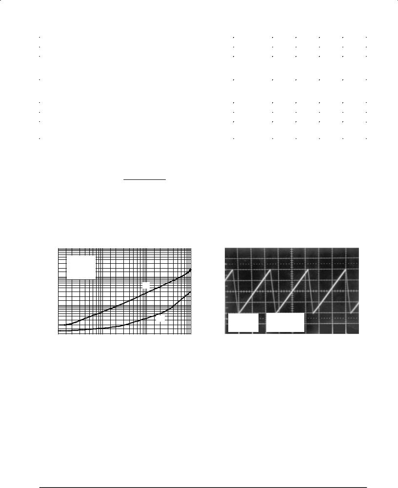
|
Figure 1. Output Switch On±Off Time versus |
|
||||||||
|
|
|
Oscillator Timing Capacitor |
|
|
|||||
μs) |
1000 |
|
|
|
|
|
|
|
|
|
|
|
|
|
|
|
|
|
|
|
|
( |
|
|
|
|
|
|
|
|
|
(V)VOLTAGE |
TIMEOFF-ON |
500 |
VCC = 5.0 V |
|
|
|
|
|
|
||
|
200 |
Pin 7 = VCC |
|
|
|
|
|
|
|
|
|
Pin 5 = Gnd |
|
|
|
|
|
|
|
||
|
|
|
|
|
|
|
|
|
||
|
100 |
TA = 25°C |
|
|
|
|
|
|
|
|
SWITCH |
50 |
|
|
|
|
|
ton |
|
|
OSCILLATOR |
20 |
|
|
|
|
|
|
|
|
||
|
|
|
|
|
|
|
|
|
|
|
OUTPUT, |
10 |
|
|
|
|
|
|
|
|
OSC |
|
|
|
|
|
|
|
|
|
||
|
5.0 |
|
|
|
|
|
|
toff |
|
, |
|
|
|
|
|
|
|
|
|
||
|
2.0 |
|
|
|
|
|
|
|
|
|
on±off |
|
|
|
|
|
|
|
|
V |
|
1.0 |
|
|
|
|
|
|
|
|
||
t |
0.01 |
0.02 |
0.05 |
0.1 |
0.2 |
0.5 |
1.0 |
2.0 |
5.0 |
10 |
|
||||||||||
|
|
|
CT, OSCILLATOR TIMING CAPACITOR (nF) |
|
|
|||||
Figure 2. Timing Capacitor Waveform
200 mV/DIV
VCC = 5.0 V |
Pins 1, 5, 8 = Open |
|
Pin 7 |
= VCC |
CT = 1.0 nF |
Pin 2 |
= Gnd |
TA = 25°C |
10 μs/DIV
MOTOROLA ANALOG IC DEVICE DATA |
3 |
|

MC34063A MC33063A
|
Figure 4. Common Emitter Configuration Output |
Figure 3. Emitter Follower Configuration Output |
Switch Saturation Voltage versus |
Saturation Voltage versus Emitter Current |
Collector Current |
VCE(sat), SATURATION VOLTAGE (V)
1.8 |
|
|
|
|
|
|
|
|
1.1 |
|
|
|
|
|
|
|
|
1.7 |
|
|
|
|
|
|
|
(V) |
1.0 |
|
|
|
|
|
|
|
|
|
|
|
|
|
|
|
0.9 |
|
|
|
|
|
Darlington Connection |
||||
|
|
|
|
|
|
|
VOLTAGE |
|
|
|
|
|
|||||
|
|
|
|
|
|
|
|
|
|
|
|
|
|||||
1.6 |
|
|
|
|
|
|
|
0.7 |
|
|
|
|
|
|
|
|
|
|
|
|
|
|
|
|
|
0.8 |
|
|
|
|
|
|
|
|
|
1.5 |
|
|
|
|
|
VCC = 5.0 V |
|
SATURATION |
0.6 |
TA = 25°C |
|
|
|
|
|
|
|
|
|
|
|
|
|
|
|
|
|
|
|
|
|
||||
1.4 |
|
|
|
|
|
|
|
|
VCC = 5.0 V |
|
|
|
|
|
|
||
|
|
|
|
|
|
|
|
|
|
|
|
|
|
|
|||
|
|
|
|
|
|
|
|
0.5 |
Pin 7 = VCC |
|
|
|
|
|
|
||
|
|
|
|
|
|
|
|
|
|
|
|
Forced β = 20 |
|
||||
1.3 |
|
|
|
|
|
|
|
|
0.4 |
Pins 2, 3, 5 = Gnd |
|
|
|
|
|||
|
|
|
|
|
|
|
|
|
|
|
|
|
|
|
|
||
1.2 |
|
|
|
|
|
Pins 1, 7, 8 = VCC |
, |
0.3 |
(See Note 4) |
|
|
|
|
|
|
||
1.1 |
|
|
|
|
|
TA = 25°C |
|
CE(sat) |
0.2 |
|
|
|
|
|
|
|
|
|
|
|
|
|
|
Pins 3, 5 = Gnd |
|
|
|
|
|
|
|
|
|
||
|
|
|
|
|
|
(See Note 4) |
|
V |
0.1 |
|
|
|
|
|
|
|
|
1.0 |
|
|
|
|
|
|
|
0 |
|
|
|
|
|
|
|
|
|
|
|
|
|
|
|
|
|
|
|
|
|
|
|
|
|
||
0 |
0.2 |
0.4 |
0.6 |
0.8 |
1.0 |
1.2 |
1.4 |
1.6 |
0 |
0.2 |
0.4 |
0.6 |
0.8 |
1.0 |
1.2 |
1.4 |
1.6 |
|
|
|
IE, EMITTER CURRENT (A) |
|
|
|
|
IC, COLLECTOR CURRENT(A) |
|
|
|||||||
Figure 5. Current Limit Sense Voltage |
Figure 6. Standby Supply Current versus |
(V) |
|
|
versus Temperature |
|
|
|
|||
400 |
|
|
|
|
|
|
|
3.6 |
|
CURRENT LIMIT SENSE VOLTAGE |
|
|
|
|
|
|
|
||
380 |
VCC = 5.0 V |
|
|
|
|
|
|
3.2 |
|
360 |
|
|
|
|
|
, SUPPLY CURRENT (mA) |
2.8 |
||
Ichg = Idischg |
|
|
|
|
|||||
340 |
|
|
|
|
|
||||
|
|
|
|
|
|
2.4 |
|||
|
|
|
|
|
|
|
|||
320 |
|
|
|
|
|
|
2.0 |
||
300 |
|
|
|
|
|
|
|||
|
|
|
|
|
|
1.6 |
|||
280 |
|
|
|
|
|
|
|||
|
|
|
|
|
|
1.2 |
|||
260 |
|
|
|
|
|
|
|||
|
|
|
|
|
|
|
|||
240 |
|
|
|
|
|
|
0.8 |
||
, |
|
|
|
|
|
|
CC |
||
|
|
|
|
|
|
|
|||
|
|
|
|
|
|
|
|
||
IPK(sense) |
220 |
|
|
|
|
|
|
I |
0.4 |
200 |
|
|
|
|
|
|
0 |
||
±55 |
±25 |
0 |
25 |
50 |
75 |
100 |
|
||
V |
125 |
|
|||||||
|
|
|
TA, AMBIENT TEMPERATURE (°C) |
|
|
|
|||
Supply Voltage
|
|
|
|
|
|
CT = 1.0 nF |
|
|
|
|
|
|
|
|
|
Pin 7 |
= VCC |
|
|
|
|
|
|
|
|
Pin 2 |
= Gnd |
|
|
0 |
5.0 |
10 |
15 |
20 |
25 |
30 |
35 |
40 |
|
VCC, SUPPLY VOLTAGE (V)
NOTE: 4. Low duty cycle pulse techniques are used during test to maintain junction temperature as close to ambient temperature as possible.
4 |
MOTOROLA ANALOG IC DEVICE DATA |
 Loading...