Philips TDA8395T-N3, TDA8395T-N2, TDA8395T-N1, TDA8395P-N2 Datasheet

INTEGRATED CIRCUITS
DATA SHEET
TDA8395
SECAM decoder
Preliminary specification |
|
October 1991 |
|||||
File under Integrated Circuits, IC02 |
|
|
|
|
|
|
|
|
|
|
|
|
|
|
|
|
|
|
|
|
|
|
|
|
|
|
|
|
|
|
|

Philips Semiconductors |
Preliminary specification |
|
|
SECAM decoder |
TDA8395 |
|
|
|
|
FEATURES
∙Fully integrated filters
∙Alignment free
∙For use with baseband delay
GENERAL DESCRIPTION
The TDA8395 is a self-calibrating, fully integrated SECAM decoder. The IC should preferably be used in conjunction with the PAL/NTSC decoder TDA8362 or TDA8366 and with the switched capacitor baseband delay circuit TDA4660. The IC incorporates HF and LF filters, a demodulator and an identification circuit (luminance is not processed in this IC). The IC needs no adjustments and very few external components are required. A highly stable reference frequency is required for calibration and a two-level sandcastle pulse for blanking and burst gating.
QUICK REFERENCE DATA
SYMBOL |
PARAMETER |
MIN. |
TYP. |
MAX. |
UNIT |
|
|
|
|
|
|
VP |
positive supply voltage; pin 3 |
7.2 |
− |
8.8 |
V |
Ptot |
total power dissipation |
− |
− |
220 |
mW |
V16(p-p) |
composite video input voltage |
− |
1.0 |
1.5 |
V |
|
(peak-to-peak value); pin 16 |
|
|
|
|
|
|
|
|
|
|
VO(p-p) |
−(R−Y) output voltage amplitude |
− |
1.05 |
− |
V |
|
(peak-to-peak value); pin 9 |
|
|
|
|
|
|
|
|
|
|
VO(p-p) |
−(B−Y) output voltage amplitude |
− |
1.33 |
− |
V |
|
(peak-to-peak value); pin 10 |
|
|
|
|
|
|
|
|
|
|
ORDERING INFORMATION
EXTENDED TYPE NUMBER |
|
|
PACKAGE |
|
|
|
|
|
|
|
|
PINS |
PIN POSITION |
|
MATERIAL |
CODE |
|
|
|
||||
|
|
|
|
|
|
TDA8395 |
16 |
DIL |
|
plastic |
SOT38GE1(1) |
Note
1. SOT38-1; 1996 December 3.
October 1991 |
2 |

Philips Semiconductors |
Preliminary specification |
|
|
SECAM decoder |
TDA8395 |
|
|
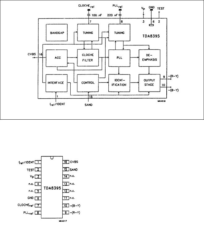
Fig.1 Block diagram.
PINNING
|
|
SYMBOL |
PIN |
DESCRIPTION |
|
|
|
|
|
|
|
fref/ IDENT |
1 |
reference frequency |
|
|
|
|
input/identification input |
|
|
|
|
|
|
|
TEST |
2 |
test output |
|
|
|
|
|
|
|
VP |
3 |
positive supply voltage |
|
|
n.c. |
4 |
not connected |
|
|
|
|
|
|
|
n.c. |
5 |
not connected |
|
|
|
|
|
|
|
GND |
6 |
ground |
|
|
|
|
|
|
|
CLOCHEref |
7 |
Cloche reference filter |
|
|
PLLref |
8 |
PLL reference |
|
|
−(R−Y) |
9 |
−(R−Y) output |
|
|
|
|
|
|
|
−(B−Y) |
10 |
−(B−Y) output |
|
|
|
|
|
|
|
n.c. |
11 |
not connected |
|
|
|
|
|
|
|
n.c. |
12 |
not connected |
|
|
|
|
|
|
|
n.c. |
13 |
not connected |
|
|
|
|
|
|
|
n.c. |
14 |
not connected |
|
|
|
|
|
Fig.2 Pin configuration |
|
SAND |
15 |
sandcastle pulse input |
|
|
|
|
|
|
CVBS |
16 |
video (chrominance) input |
|
|
|
|||
|
|
|
|
|
|
|
|
|
|
October 1991 |
3 |
 Loading...