


 Loading...
INTEGRATED CIRCUITS
DATA SHEET
TEA1507
GreenChipäII SMPS control IC
Preliminary specification |
|
2000 Dec 05 |
|||||
File under Integrated Circuits, IC11 |
|
|
|
|
|
|
|
|
|
|
|
|
|
|
|
|
|
|
|
|
|
|
|
|
|
|
|
|
|
|
|

Philips Semiconductors |
Preliminary specification |
|
|
|
GreenChipäII SMPS control IC |
|
TEA1507 |
|
FEATURES |
|
|
||
Distinctive features |
|
|
||
∙ |
Universal mains supply operation (70 to 276 V AC) |
|
|
|
∙ |
High level of integration, giving a very low external |
|
|
|
|
component count. |
handbook, halfpage |
|
|
|
|
|
||
Green features |
|
|
||
∙ |
Valley/zero voltage switching for minimum switching |
|
|
|
|
losses |
|
|
|
∙ |
Efficient quasi-resonant operation at high power levels |
1 |
8 |
|
|
|
|||
∙ |
Frequency reduction at low power standby for improved |
2 |
7 |
|
|
system efficiency (<3 W) |
TEA1507 |
||
∙ |
Burst mode operation for very low standby levels (<1 W) |
3 |
6 |
|
|
|
|||
∙ |
On-chip start-up current source. |
4 |
5 |
|
Protection features |
|
|
||
∙ |
Safe restart mode for system fault conditions |
|
|
|
∙ |
Continuous mode protection by means of |
|
|
|
|
demagnetization detection (zero switch-on current) |
|
|
|
∙ |
Accurate and adjustable overvoltage protection |
|
|
|
∙ |
Short winding protection |
|
|
|
∙ |
Undervoltage protection (foldback during overload) |
|
|
|
∙ |
Overtemperature protection |
|
|
|
∙ |
Low and adjustable overcurrent protection trip level |
|
|
|
∙ |
Soft (re)start |
|
MGU229 |
|
|
|
|
||
∙ |
Mains voltage-dependent operation-enabling level. |
|
|
|
APPLICATIONS |
|
|
||
Besides typical application areas, i.e. TV and Monitor |
|
|
||
supplies, the device can be used in all applications that |
|
|
||
demand an efficient and cost-effective solution up to |
Fig.1 |
Typical application. |
||
250 W. |
||||
|
|
|||
2000 Dec 05 |
2 |

Philips Semiconductors |
Preliminary specification |
|
|
GreenChipäII SMPS control IC |
TEA1507 |
|
|
GENERAL DESCRIPTION
The GreenChipäII is the second generation of green Switched Mode Power Supply (SMPS) controller ICs operating directly from the rectified universal mains. A high level of integration leads to a cost effective power supply with a very low number of external components.
The special built-in green functions allow the efficiency to be optimum at all power levels. This holds for quasi-resonant operation at high power levels, as well as fixed frequency operation with valley switching at medium power levels. At low power (standby) levels, the system operates at reduced frequency and with valley detection.
If burst mode operation is applied, the standby power level can even be reduced to below 1 W.
The proprietary high voltage BCD800 process makes direct start-up possible from the rectified mains voltage in an effective and green way. A second low voltage BICMOS IC is used for accurate, high speed protection functions and control.
Highly efficient, reliable supplies can easily be designed using the GreenChipäII controller.
ORDERING INFORMATION
TYPE |
|
PACKAGE |
|
|
|
|
|
NUMBER |
NAME |
DESCRIPTION |
VERSION |
|
|||
|
|
|
|
TEA1507P |
DIP8 |
plastic dual in-line package; 8 leads (300 mil) |
SOT97-1 |
|
|
|
|
2000 Dec 05 |
3 |

_ |
|
|
|
|
|
|
|
|
|
05 Dec 2000 |
|
SUPPLY |
|
|
pagewidth full andbook, |
|
|
8 |
DIAGRAMBLOCK |
1 |
|
|
|
START-UP |
|
|
DRAIN |
||
VCC |
|
MANAGEMENT |
|
|
CURRENT SOURCE |
|
|
|
|
|
|
|
|
|
|
|
|
||
|
|
internal UVLO start |
|
|
|
clamp |
|
7 |
HVS |
|
|
|
|
VALLEY |
|
|
|
n.c. |
|
|
|
supply |
|
|
|
|
|
||
|
M-level |
|
|
|
|
|
|
||
|
|
|
|
|
|
|
|
|
|
2 |
S1 |
VOLTAGE |
|
|
|
|
|
4 |
DEM |
|
|
|
|
|
|
||||
GND |
|
CONTROLLED |
LOGIC |
|
|
|
|
|
|
|
|
|
|
|
|
|
|||
|
|
|
|
|
|
|
|
||
|
|
OSCILLATOR |
|
|
|
|
|
|
|
|
|
|
|
|
100 mV |
|
|
|
|
|
|
|
|
|
|
OVER- |
|
|
|
|
|
FREQUENCY |
|
|
|
VOLTAGE |
|
|
|
|
|
CONTROL |
|
|
|
PROTECTION |
|
|
|
|
|
OVER- |
LOGIC |
|
DRIVER |
|
6 |
DRIVER |
|
4 |
|
TEMPERATURE |
|
|
|
||||
|
|
|
|
|
|
|
|
||
|
PROTECTION |
|
|
|
|
|
|
|
|
|
|
|
|
|
|
|
|
|
|
3 |
|
|
|
|
|
|
|
Iss |
|
−1 |
POWER-ON |
|
|
|
LEB |
|
|
|
|
CTRL |
S |
Q |
|
soft |
0.5 V |
|
|||
|
|
RESET |
|
|
|
||||
|
|
|
|
|
|
||||
|
|
|
|
|
|
start |
|
|
|
|
|
|
|
|
|
blank |
|
|
|
|
|
|
|
|
|
S2 |
|
|
|
|
|
|
|
|
|
|
|
|
|
|
2.5 V |
UVLO |
R |
Q |
|
|
|
5 |
|
|
|
|
|
|
|
|
Isense |
||
|
|
|
|
|
|
OCP |
|
|
|
|
burst |
|
|
|
|
|
|
|
|
|
|
|
|
|
|
|
|
|
|
|
detect |
|
|
|
|
|
|
|
|
|
|
MAXIMUM |
|
|
short |
0.75 V |
|
|
|
|
|
|
|
winding |
|
|
|
||
|
|
ON-TIME |
|
|
|
|
|
||
|
|
|
|
|
|
|
|
|
|
|
TEA1507 |
PROTECTION |
|
|
|
|
|
|
|
|
|
|
|
|
OVERPOWER |
|
|
||
|
|
|
|
|
|
|
|
||
|
|
|
|
|
|
PROTECTION |
|
|
|
|
|
|
|
|
|
|
|
MGU230 |
|
Fig.2 Block diagram.
IC control SMPS IIäGreenChip
TEA1507
Semiconductors Philips
specification Preliminary
Philips Semiconductors |
Preliminary specification |
|
|
GreenChipäII SMPS control IC |
TEA1507 |
|
|
PINNING
SYMBOL |
PIN |
DESCRIPTION |
|
|
|
VCC |
1 |
supply voltage |
GND |
2 |
ground |
|
|
|
CTRL |
3 |
control input |
|
|
|
DEM |
4 |
input from auxiliary winding for |
|
|
demagnetization timing, OVP and OPP |
|
|
|
Isense |
5 |
programmable current sense input |
DRIVER |
6 |
gate driver output |
|
|
|
HVS |
7 |
high voltage safety spacer, not |
|
|
connected |
|
|
|
DRAIN |
8 |
drain of external MOS switch, input for |
|
|
start-up current and valley sensing |
|
|
|
FUNCTIONAL DESCRIPTION
The TEA1507 is the controller of a compact flyback converter, with the IC situated at the primary side. An auxiliary winding of the transformer provides demagnetization detection and powers the IC after start-up.
The TEA1507 operates in multi modes.
The next converter stroke is started only after demagnetization of the transformer current (zero current switching), while the drain voltage has reached the lowest voltage to prevent switching losses (green function). The primary resonant circuit of primary inductance and drain capacitor ensures this quasi-resonant operation. The design can be optimized in such a way that zero voltage switching can be reached over almost the universal mains range.
To prevent very high frequency operation at lower loads, the quasi-resonant operation changes smoothly in fixed frequency PWM control.
At very low power (standby) levels, the frequency is controlled down, via the VCO, to a minimum frequency of about 6 kHz. Typically, 3 Watts can be achieved for a
75 W converter with an output power of 100 mW.
Start-up, mains enabling operation level and undervoltage lock out (see Figs. 10 and 11)
Initially, the IC is self supplying from the rectified mains voltage via pin DRAIN. Supply capacitor CVCC is charged by the internal start-up current source to a level of about 4 V or higher, depending on the drain voltage. Once the drain voltage exceeds the M-level (mains-dependent operation-enabling level), the start-up current source will
handbook, halfpage
VCC |
1 |
|
|
8 |
DRAIN |
||
|
|
|
|
|
|
|
|
GND |
2 |
|
7 |
HVS |
|||
|
|
|
TEA1507 |
|
|
|
|
CTRL |
3 |
|
|
|
6 |
DRIVER |
|
|
|
|
|
|
|
|
|
DEM |
4 |
|
5 |
Isense |
|||
|
|
|
|
|
|
|
|
|
|
|
MGU231 |
|
|||
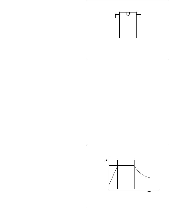
Fig.3 Pin configuration.
continue charging capacitor CVCC (switch S1 will be opened), see Fig.2. The IC will activate the power converter as soon as the voltage on pin VCC passes the
VCC(start) level. The IC supply is taken over by the auxiliary winding as soon as the output voltage reaches its intended
level and the IC supply from the mains voltage is subsequently stopped for high efficiency operation (green function).
The moment the voltage on pin VCC drops below the VUVLO (undervoltage lock out) level, the IC stops switching and enters a safe restart from the rectified mains voltage. Inhibiting the auxiliary supply by external means causes the converter to operate in a stable, well-defined burst mode.
Supply management
All (internal) reference voltages are derived from a temperature compensated, on-chip band gap circuit.
f |
|
MGU232 |
|
handbook, halfpage |
VCO |
fixed |
quasi resonant |
|
|||
|
|||
175 kHz |
|
|
|
6 kHz
power
Fig.4 Multi mode operation.
2000 Dec 05 |
5 |

Philips Semiconductors |
Preliminary specification |
|
|
GreenChipäII SMPS control IC |
TEA1507 |
|
|
Current mode control
Current mode control is used for its good line regulation behaviour.
The ‘on-time’ is controlled by the internally inverted control pin voltage, which is compared with the primary current information. The primary current is sensed across an external resistor. The driver output is latched in the logic, preventing multiple switch-on.
As soon as the oscillator voltage is high again and the secondary stroke has ended, the circuit waits for the lowest drain voltage before starting a new primary stroke. This method is called valley detection. Figure 7 shows the drain voltage together with the valley signal, the signal indicating the secondary stroke and the oscillator signal.
In an optimum design, the reflected secondary voltage on the primary side will force the drain voltage to zero. Thus, zero voltage switching is very possible, preventing large
The internal control voltage is inversely proportional to the external control pin voltage, with an offset of 1.5 V. This means that a voltage range from 1 to 1.5 V on pin CTRL will result in an internal control voltage range from
0.5 to 0 V (the maximum external control voltage results in a minimum duty cycle).
Oscillator
The maximum fixed frequency of the oscillator is set by an internal current source and capacitor. The maximum frequency is reduced once the control voltage enters the VCO control window. Then, the maximum frequency changes linearly with the control voltage until the minimum frequency is reached (see Figs 5 and 6).
Valley switching (see Fig.7)
A new cycle starts when the power switch is switched on. After the ‘on-time’ (which is determined by the ‘sense’ voltage and the internal control voltage), the switch is opened and the secondary stroke starts. After the secondary stroke, the drain voltage shows an oscillation
|
1 |
with a frequency of approximately |
(----------------------------------------------------2 ´ p ´ (Lp ´ Cd)) |
where Lp is the primary self inductance of the transformer and Cd is the capacitance on the drain node.
|
1 |
´ C ´ V |
2 |
´ fö |
, and |
capacitive switching losses æP = -- |
|
||||
è |
2 |
|
|
ø |
|
allowing high frequency operation, which results in small and cost effective inductors.
Demagnetization
The system will be in discontinuous conduction mode all the time. The oscillator will not start a new primary stroke until the secondary stroke has ended.
Demagnetization features a cycle-by-cycle output short-circuit protection by immediately lowering the frequency (longer off-time), thereby reducing the power level.
Demagnetization recognition is suppressed during the first
tsuppr time. This suppression may be necessary in applications where the transformer has a large leakage
inductance and at low output voltages/start-up.
Minimum and maximum ‘on-time’
The minimum ‘on-time’ of the SMPS is determined by the Leading Edge Blanking (LEB) time. The IC limits the ‘on-time’ to 50 ms. When the system desires an ‘on-time’ longer than 50 ms, a fault condition is assumed (e.g. removed Ci), the IC will stop switching and enter the safe restart mode.
MGU233
Vsense(max) handbook, halfpage
0.5 V
1 V |
1.5 V |
|
VCTRL |
|
|||
(typ) |
(typ) |
|
|
Fig.5 The Vsense(max) voltage as function of VCTRL.
MGU234
handbook, halfpage f
175 kHz
6 kHz
50 mV |
75 mV Vsense(max) |
||
(typ) |
(typ) |
|
|
|
|||
Fig.6 The VCO frequency as function of Vsense(max)
2000 Dec 05 |
6 |
Loading...