


UAA3220TS

DATA SH EET
Product specification
Supersedes data of 1998 April 10
File under Integrated Circuits, IC01
1999 Jan 22
INTEGRATED CIRCUITS
UAA3220TS
Frequency Shift Keying
(FSK)/Amplitude Shift Keying
(ASK) receiver

1999 Jan 22 2
Philips Semiconductors Product specification
Frequency Shift Keying (FSK)/Amplitude
Shift Keying (ASK) receiver
UAA3220TS
FEATURES
• Low cost single-chip ASK or FSK receiver
• Superheterodyne architecture with high integration level
• Few external low cost components and crystal required
• Wide supply voltage range
• Low power consumption
• Wide frequency range, 250 to 920 MHz
• High sensitivity
• IF bandwidth determined by application
• High selectivity
• Automotive temperature range
• SSOP24 package.
Applications
• Keyless entry systems
• Car alarm systems
• Remote control systems
• Security systems
• Telemetry systems
• Wireless data transmission
• Domestic appliance.
GENERAL DESCRIPTION
The UAA3220TS is a fully integrated single-chip receiver,
primarily intended for use in VHF and UHF systems.
It supports both Amplitude Shift Keying (ASK) and
Frequency Shift Keying (FSK) demodulation.
By connecting DEMO1 (pin 10) to ground during
realisation of the receiver module the UAA3220TS works
as an ASK receiver (see Fig.10). By connecting pin 10 as
shown in Fig.9 the UAA3220TS works as an FSK receiver.
The UAA3220TS incorporates a crystal stabilized local
oscillator, frequency multiplier, balanced mixer, post mixer
amplifier, limiter, Received Signal Strength Indicator
(RSSI), FSK demodulator, data filter, data slicer and
power down circuit.
QUICK REFERENCE DATA
SYMBOL PARAMETER CONDITIONS MIN. TYP. MAX. UNIT
V
CC
supply voltage 2.7 − 5.5 V
I
CC
supply current f
i(RF)
= 433.92 MHz; FSK mode
operating mode on;
V
PWD
=0V
2.8 4.3 5.8 mA
operating mode off;
V
PWD
=V
CC
− 330µA
ASK mode
P
i(max)(ASK)
maximum input power BER ≤ 3% −22 −16 −10 dBm
Φ
i(ASK)
sensitivity into pin MIXIN f
i(RF)
= 433.92 MHz; BER ≤ 3% −−119 −113 dBm
FSK mode
P
i(max)(FSK)
maximum input power BER ≤ 3% −6 0 +1 dBm
Φ
i(FSK)
sensitivity into pin MIXIN f
i(RF)
= 433.92 MHz; BER ≤ 3% −−103 −100 dBm

1999 Jan 22 3
Philips Semiconductors Product specification
Frequency Shift Keying (FSK)/Amplitude
Shift Keying (ASK) receiver
UAA3220TS
ORDERING INFORMATION
BLOCK DIAGRAM
TYPE
NUMBER
PACKAGE
NAME DESCRIPTION VERSION
UAA3220TS SSOP24
plastic shrink small outline package; 24 leads; body width 5.3 mm
SOT340-1
Fig.1 Block diagram.
handbook, full pagewidth
MGM742
PMA
DEMODULATOR
AM/FM
SWITCH
DATA SLICER
MIXER
BIAS
22
FA
23
MIXIN
24
MGND
16 1518
CPB
17
CPC CPA
11
DEMO2
12
GND
10
DEMO1
9
PWD
MULTIPLIER
×3
7
TN
8
TP
6
TEM
OSCILLATOR
2
OSE
3
OSB
4
V
CC
5
OSC
1
OGND
RSSILIN
V
CCI
21 20
LFB
19
DATA
14
CGND
13
LIMITER
AMPLIFIER
−
+
UAA3220TS
×2/×3
1999 Jan 22 4
Philips Semiconductors Product specification
Frequency Shift Keying (FSK)/Amplitude
Shift Keying (ASK) receiver
UAA3220TS
PINNING
SYMBOL PIN DESCRIPTION
OGND 1 oscillator ground
OSE 2 oscillator emitter
OSB 3 oscillator base
V
CC
4 positive supply voltage
OSC 5 oscillator collector
TEM 6 frequency multiplier emitter resistor
TN 7 frequency multiplier negative output
TP 8 frequency multiplier positive output
PWD 9 power down control input
DEMO1 10 FM demodulator 1, ASK/FSK switch
DEMO2 11 FM demodulator 2
GND 12 general ground
CGND 13 comparator ground
DATA 14 data output
CPA 15 comparator input A
CPB 16 comparator input B
CPC 17 comparator input C
RSSI 18 RSSI output
LFB 19 limiter feedback
LIN 20 limiter input
V
CCI
21 IF amplifier positive supply voltage
FA 22 IF amplifier output
MIXIN 23 mixer input
MGND 24 mixer ground
Fig.2 Pin configuration.
handbook, halfpage
OGND
OSE
OSB
V
CC
OSC
TEM
TN
TP
PWD
DEMO1
DEMO2
GND
MGND
MIXIN
FA
V
CCI
LFB
RSSI
LIN
CPC
CPB
CPA
DATA
CGND
1
2
3
4
5
6
7
8
9
10
11
12
24
23
22
21
20
19
18
17
16
15
14
13
UAA3220TS
MGM743

1999 Jan 22 5
Philips Semiconductors Product specification
Frequency Shift Keying (FSK)/Amplitude
Shift Keying (ASK) receiver
UAA3220TS
FUNCTIONAL DESCRIPTION
Mixer
The mixer is a single-balanced emitter-coupled mixer with
internal biasing. Matching of the RF source impedance to
the mixer input requires an external matching network.
Oscillator
The oscillator is based on a transistor connected in
common collector configuration followed by a cascode
stage driving a tuned circuit. The voltage at this tuned
circuit drives the frequency multiplier. The bias current of
the oscillator is set by an off-chip resistor (R40 in the
application diagram of Fig.9) to a typical value of 260 µA at
433.92 MHz (R40 = 1.8 kΩ). The oscillator frequency is
controlled by an off-chip overtone crystal (X40). Off-chip
capacitors between base and emitter (C42) and ground
(C41) make the oscillator transistor appear as having
negative resistance at small signal levels. This causes the
oscillator to start. A parallel resonance circuit (L40 and
C41) connected to the emitter of the oscillator transistor
prevents oscillation at the fundamental frequency of the
crystal. The LC tank circuit at the output of the oscillator is
used to select either the fundamental, the second or the
third harmonic of the oscillator frequency.
Frequency multiplier
The frequency multiplier is an emitter-coupled transistor
pair driving an off-chip balanced tuned circuit. The bias
current of this emitter coupled pair is set by an off-chip
resistor (R50) to a typical value of 350 µA at 433.92 MHz
(R50 = 1.2 kΩ). The oscillator output signal is AC-coupled
to one of the inputs of the emitter-coupled pair. The other
input is connected to ground via an on-chip capacitor.
The output voltage of the frequency multiplier drives the
switching stage of the mixer. The bias voltage at this point
is set by an off-chip resistor (R51) to allow sufficient
voltage swing at the mixer outputs.
Post mixer amplifier
The Post Mixer Amplifier (PMA) is a differential input,
single-ended output amplifier. Amplifier gain is provided in
order to reduce the influence of the limiter noise figure on
the total noise figure.
Limiter
The limiter is a single-ended input multiple stage amplifier
with high total gain. Amplifier stability is achieved by
means of an external DC feedback capacitor (C21), which
is also used to determine the lower limiter cut-off
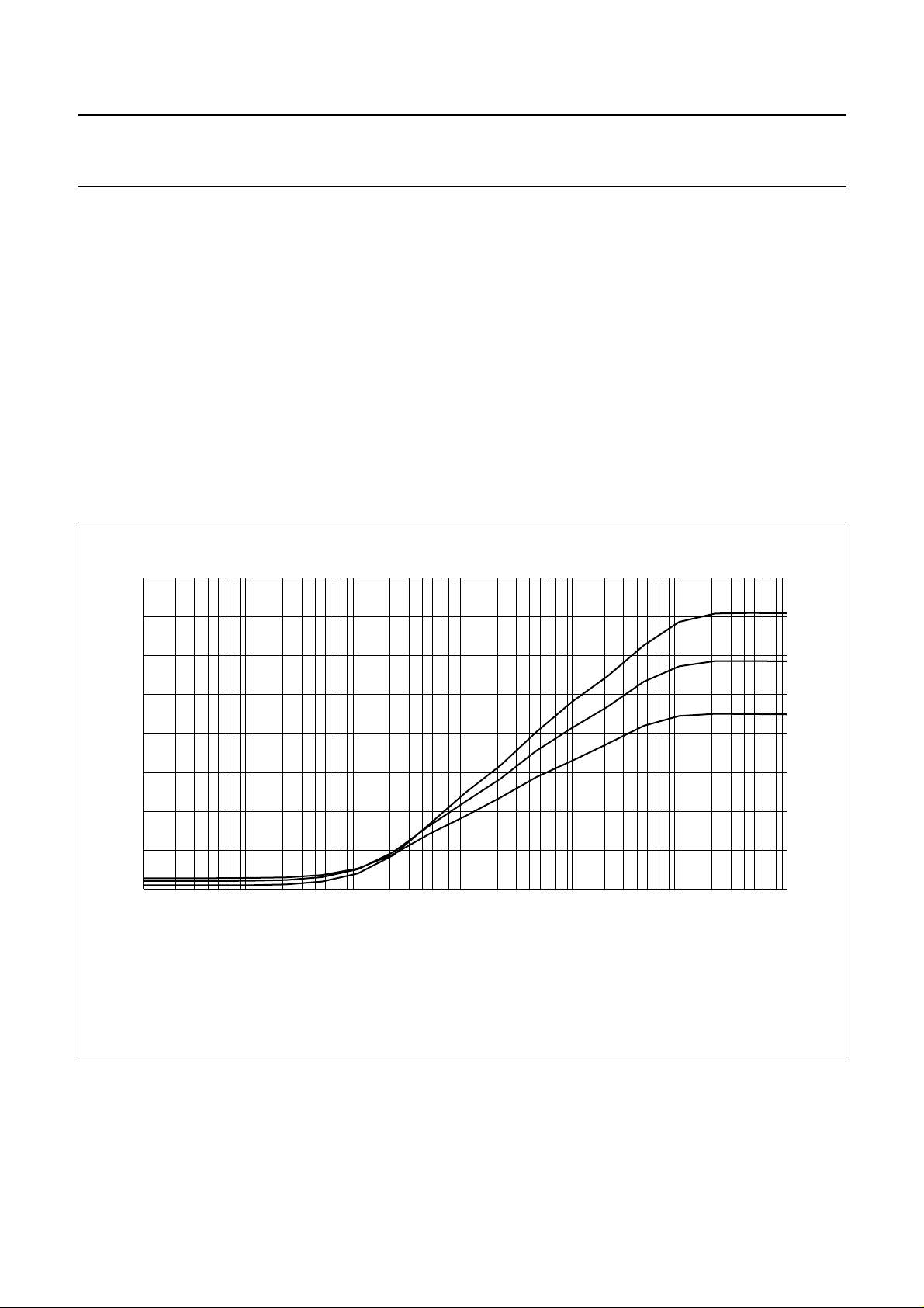
frequency. An RSSI signal proportional to the limiter input
signal is provided. Figure 3 shows the DC voltage at pin 18
(RSSI) as a function of the input voltage (RMS value) at
pin 20 (LIN). It also gives the typical IF of 10.7 MHz.
The lower knee of the level curve (see Fig.3) is determined
by the effective noise bandwidth and is, consequently,
slightly higher.
IF filter
IF filtering with high selectivity is realized by means of an
external ceramic filter (X20), which feeds the IF from the
PMA to the limiter.
FM demodulator
Coming from the limiter the FSK signal is fed differential to
the input of the FM demodulator. After buffering the signal
is fed to a phase detector. The phase shift is generated by
an external LC combination connected to DEMO1 (pin 10)
and DEMO2 (pin 11). The baseband signal is coupled out
single ended via an output buffer and is fed to the FSK
input of the ASK/FSK switch.
ASK/FSK switch
The selection of either ASK or FSK reception will be done
by the DEMO1 (pin 10). Grounding this pin to 0 V will
switch the IC to ASK mode. Additional the FM demodulator
and parts of the data slicer will be switched off. In FSK
mode DEMO1 (pin 10) is connected to DEMO2 (pin 11)
via a LC combination (see Fig.9).
Data filters
After demodulation a two-stage data filtering circuit is
provided in order to suppress unwanted frequency
components. Two RC low-pass filters with on-chip
resistors are provided which are separated by a buffer
stage.
1999 Jan 22 6
Philips Semiconductors Product specification
Frequency Shift Keying (FSK)/Amplitude
Shift Keying (ASK) receiver
UAA3220TS
Data slicer
Data detection is provided by means of a level comparator
with adaptive slice reference. After the first data filter stage
the pre-filtered data is split into two paths. One passes the
second data filter stage and is fed to the positive
comparator input. The other path is fed to an integration
circuit with a large time constant in order to derive the
average value (DC component) as an adaptive slice
reference which is presented to the negative comparator
input. The internal buffer provides 13 dB AC voltage gain.
The adaptive reference allows to detect the received data
over a large range of noise floor levels. The integration
circuit consists of a simple RC low-pass filter with on-chip
resistors. The data slicer output is designed with internal
pull-up.
RSSI buffer
The RSSI buffer is an amplifier with a voltage gain of 0 dB.
At FSK receive mode the RSSI output provides a field
strength indication. It has an output impedance of 10 kΩ.
Figure 3 shows the level curve (RSSI curve) as a function
of the limiter input voltage (RMS value).
Fig.3 Level curve V
RSSI
as a function of V
LIN(rms)
.
handbook, full pagewidth
1.55
1.25
1.15
1.45
1.35
MGM744
10
-7
10
-6
10
-5
10
-4
10
-3
10
-2
10
-1
V
RSSI
(V)
V
LIN(rms)
(V)
(1)
(2)
(3)
(1) T
amb
=85°C.
(2) T
amb
=27°C.
(3) T
amb
= −40°C.

1999 Jan 22 7
Philips Semiconductors Product specification
Frequency Shift Keying (FSK)/Amplitude
Shift Keying (ASK) receiver
UAA3220TS
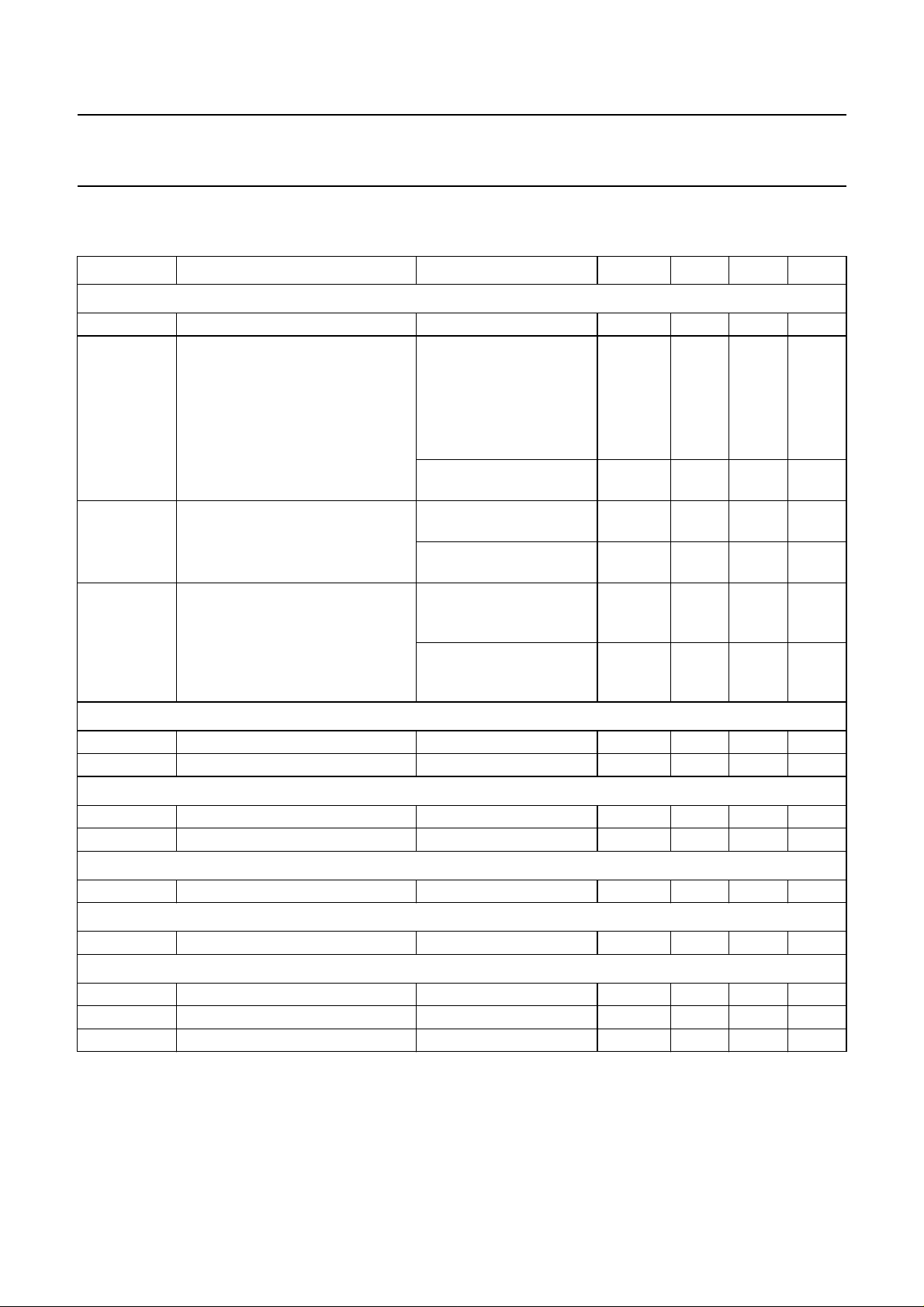
LIMITING VALUES
In accordance with the Absolute Maximum Rating System (IEC 134).
Note
1. Machine model: C = 200 pF, R = 0 Ω and L = 0.75 µH; pins are connected to GND and V
CC
.
THERMAL CHARACTERISTICS
SYMBOL PARAMETER CONDITIONS MIN. MAX. UNIT
V
CC
supply voltage −0.3 +8.0 V
P
i(max)
absolute maximum input power − 3 dBm
T
amb
operating ambient temperature −40 +85 °C
T
stg
storage temperature −55 +125 °C
V
es
electrostatic handling note 1
pins 3 and 6 −50 +50 V
pin 2 −100 +100 V
pin 5 −250 +150 V
pin 23 −200 +250 V
all other pins −250 +250 V
SYMBOL PARAMETER CONDITIONS VALUE UNIT
R
th(j-a)
thermal resistance from junction to ambient in free air 125 K/W
1999 Jan 22 8
Philips Semiconductors Product specification
Frequency Shift Keying (FSK)/Amplitude
Shift Keying (ASK) receiver
UAA3220TS
DC CHARACTERISTICS
V
CC
= 2.7 V; T
amb
=25°C; for application diagram see Figs 9 and 10; crystal disconnected; unless otherwise specified.
SYMBOL PARAMETER CONDITIONS MIN. TYP. MAX. UNIT
Supplies
V
CC
supply voltage 2.7 − 5.5 V
I
CC
supply current operating mode on;
V
PWD
= 0 V; notes 1 and 2
FSK demodulation;
note 3
2.8 4.3 5.8 mA
ASK demodulation;
note 4
2.5 3.7 4.9 mA
operating mode off;
V
PWD
=V
CC
− 330µA
V
PWD
voltage on pin PWD operating mode on
(receiving mode)
0 − 300 mV
operating mode off
(sleep mode)
V
CC
− 0.3 − V
CC
V
I
PWD
current into pin PWD operating mode on
(receiving mode);
V
PWD
=0V
−30 −10 −3 µA
operating mode off
(sleep mode);
V
PWD
=V
CC
− 215µA
Oscillator
V
OSE
DC voltage at pin 2 independent of oscillator 0.33 0.38 0.43 V
V
OSB
DC voltage at pin 3 independent of oscillator 1.05 1.15 1.25 V
Multiplier
V
TEM
DC voltage at pin 6 independent of oscillator 0.33 0.39 0.45 V
V
TN,TP
DC voltage at pins 7 and 8 independent of oscillator 2.01 2.21 2.41 V
Mixer
V
MIXIN
DC voltage at pin 23 independent of oscillator 0.68 0.78 0.88 V
Post mixer amplifier
V
FA
DC voltage at pin 22 independent of oscillator 1.10 1.25 1.40 V
Limiter
V
LIN
DC voltage at pin 20 independent of oscillator 1.85 1.95 2.05 V
V
LFB
DC voltage at pin 19 independent of oscillator 1.85 1.95 2.05 V
V
RSSI
DC voltage at pin 18 independent of oscillator 1.00 1.16 1.32 V

1999 Jan 22 9
Philips Semiconductors Product specification
Frequency Shift Keying (FSK)/Amplitude
Shift Keying (ASK) receiver
UAA3220TS
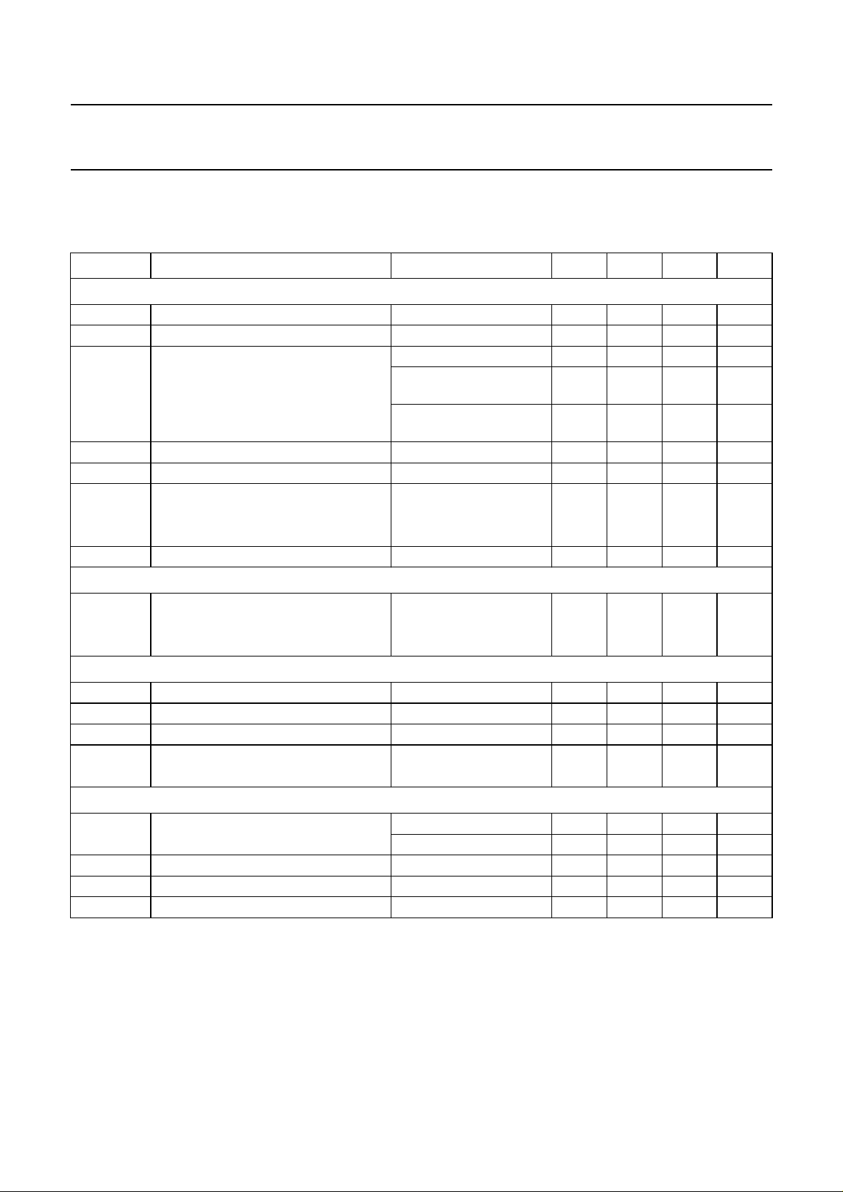
Notes
1. For f
i(RF)
= 868.35 MHz all values + 0.6 mA.
2. Crystal connected; oscillator and multiplier active.
3. Pin DEMO1 connected to pin DEMO2 via tank circuit.
4. Pin DEMO1 short circuited to ground.
5. The given values are applicable for FSK reception mode. In ASK mode pin 10 is short circuited to ground.
6. No modulation and f
IF
= 10.7 MHz.
Demodulator
V
DEMO1,2
DC voltage at pins 10 and 11 independent of oscillator;
note 5
2.00 2.24 2.48 V
V
DEMO1(ASK)
DC voltage at pin 10 to switch in
ASK mode
0 − 300 mV
Data filter and slicer
V
CPA,CPB,CPC
DC voltage at pins 15, 16 and 17 ASK mode 1.27 1.42 1.57 V
FSK mode; note 6 1.81 2.01 2.21 V
V
OH(DATA)
HIGH-level output voltage at pin 14 I
DATA
= −10 µAV
CC
− 0.5 − V
CC
V
V
OL(DATA)
LOW-level output voltage at pin 14 I
DATA
= 200 µA0−0.6 V
SYMBOL PARAMETER CONDITIONS MIN. TYP. MAX. UNIT
1999 Jan 22 10
Philips Semiconductors Product specification
Frequency Shift Keying (FSK)/Amplitude
Shift Keying (ASK) receiver
UAA3220TS
AC CHARACTERISTICS
V
CC
= 2.7 V; T
amb
=25°C; for application diagram see Figs 9 and 10; f
i(RF)
= 433.92 MHz (see Table 4) and
f
i(RF)
= 868.35 MHz (see Table 5); f
mod
= 1 kHz square wave; unless otherwise specified.
SYMBOL PARAMETER CONDITIONS MIN. TYP. MAX. UNIT
System performance
f
i(RF)
RF input frequency 250 − 920 MHz
f
IF
IF frequency 10.56 10.7 10.84 MHz
P
i(max)
maximum input power −−3 dBm
ASK mode; BER ≤ 3%;
notes 1 and 2
−22 −16 −10 dBm
FSK mode; BER ≤ 3%;
notes 2 and 3
−6 0 +1 dBm
P
SPUR
spurious radiation note 4 −−−57 dBm
f
DATA
data frequency note 5 − 1 − kHz
t
on(RX)
receiver turn-on time notes 6 and 7
f
i(RF)
= 433.92 MHz − 610ms
f
i(RF)
= 868.35 MHz − 37ms
V
RSSI
RSSI voltage 1.1 − 1.6 V
ASK mode
Φ
i(ASK)
input sensitivity directly into pin MIXIN BER ≤ 3%; notes 1 and 2
f
i(RF)
= 433.92 MHz −−119 −113 dBm
f
i(RF)
= 868.35 MHz −−116 −110 dBm
FSK mode
Φ
i(FSK)
input sensitivity directly into pin MIXIN BER ≤ 3%; notes 2 and 3 −−103 −100 dBm
∆f frequency deviation (peak value) 4 10 75 kHz
∆Φ
(FSK)(max)
maximum sensitivity degradation ∆f=4kHz −−3dB
G
dem
demodulator gain note 8 0.75 1.0 1.25
Mixer and post mixer amplifier
Z
i
input impedance of mixer f
i(RF)
= 433.92 MHz − 600 −Ω
f
i(RF)
= 868.35 MHz − 300 −Ω
IP3
PMA
interception point (mixer + PMA) −38 −30 − dBm
G
PMA
gain (mixer + PMA) note 9 40 42 50 dB
Z
o(IF)
output impedance of IF amplifier 280 330 380 Ω
mV
kHz
--------- -
 Loading...