


INTEGRATED CIRCUITS
DATA SHEET
TDA1305T
Stereo 1fs data input up-sampling filter with bitstream continuous dual DAC (BCC-DAC2)
Preliminary specification |
1995 Dec 08 |
Supersedes data of September 1994
File under Integrated Circuits, IC01

Philips Semiconductors |
Preliminary specification |
|
|
Stereo 1fs data input up-sampling filter with
TDA1305T
bitstream continuous dual DAC (BCC-DAC2)
FEATURES
∙Easy application
∙16fs Finite-duration Impulse-Response (FIR) filter incorporated
∙Selectable system clock (fsys) 256fs or 384fs
∙I2S-bus serial input format (at fsys = 256fs) or LSB fixed 16, 18 or 20 bits serial input mode (at fsys = 384fs)
∙Slave-mode clock system
∙Cascaded 4-stage digital filter incorporating 2-stage FIR filter, linear interpolator and sample-and-hold
∙Smoothed transitions before and after muting (soft mute)
bitstream converter for low signals while large signals are generated using the dynamic continuous calibration technique, thus resulting in low power consumption, small chip size and easy application.
∙Digital de-emphasis filter for three sampling rates of 32 kHz, 44.1 kHz and 48 kHz
∙12 dB attenuation via the attenuation input control
∙Double speed mode
∙2nd order noise shaper
∙96 (fsys = 384fs) or 128 (fsys = 256fs) times oversampling in normal speed mode
∙48 (fsys = 384fs) or 64 (fsys = 256fs) times oversampling in double speed mode
∙Bitstream continuous calibration concept
∙Small outline SO28 package
∙Voltage output 1.5 V (RMS) at line drive level
∙Low total harmonic distortion
∙No zero crossing distortion
∙Inherently monotonic
∙No analog post filtering required
∙Superior signal-to-noise ratio
∙Wide dynamic range (18-bit)
∙Single rail supply (3.4 to 5.5 V).
GENERAL DESCRIPTION
The TDA1305T is a new generation of filter-DAC which features a unique combination of bitstream and continuous calibration techniques. The converter functions as a
The TDA1305T is a dual CMOS DAC with up-sampling filter and noise shaper. The combination of high oversampling up to 16fs, 2nd order noise shaping and continuous calibration conversion ensures that only simple 1st order analog post filtering is required.
The TDA1305T supports the I2S-bus data input mode with
word lengths of up to 20 bits (at fsys = 256fs) and the LSB fixed serial data input format with word lengths of 16, 18
and 20 bits (at fsys = 384fs). Four cascaded FIR filters increase the oversampling rate to 16 times. A sample-and-hold function increases the oversampling rate
to 96 times (fsys = 384fs) or 128 times (fsys = 256fs). A 2nd order noise shaper converts this oversampled data to
a bitstream for the 5-bit DACs.
The DACs are of the continuous calibration type and incorporate a special date coding. This ensures an extremely high signal-to-noise ratio, superior dynamic range and immunity to process variation and component ageing.
Two on-board operational amplifiers convert the digital-to-analog current to an output voltage. Externally connected capacitors perform the required 1st order filtering so that no further post filtering is required.
The unique combination of bitstream and continuous calibration techniques, together with a high degree of analog and digital integration, results in a single filter-DAC with 18-bit dynamic range, high linearity and simple low cost application.
ORDERING INFORMATION
TYPE NUMBER |
|
PACKAGE |
|
|
|
|
|
||
NAME |
DESCRIPTION |
VERSION |
||
|
||||
|
|
|
|
|
TDA1305T |
SO28 |
plastic small outline package; 28 leads; body width 7.5 mm |
SOT136-1 |
|
|
|
|
|
1995 Dec 08 |
2 |

Philips Semiconductors |
Preliminary specification |
|
|
Stereo 1fs data input up-sampling filter with
TDA1305T
bitstream continuous dual DAC (BCC-DAC2)
QUICK REFERENCE DATA
SYMBOL |
PARAMETER |
CONDITIONS |
MIN. |
TYP. |
MAX. |
UNIT |
|
|
|
|
|
|
|
VDDD |
digital supply voltage |
note 1 |
3.4 |
5.0 |
5.5 |
V |
VDDA |
analog supply voltage |
note 1 |
3.4 |
5.0 |
5.5 |
V |
VDDO |
operational amplifier |
note 1 |
3.4 |
5.0 |
5.5 |
V |
|
supply voltage |
|
|
|
|
|
|
|
|
|
|
|
|
IDDD |
digital supply current |
VDDD = 5 V; |
− |
30 |
− |
mA |
|
|
at code 00000H |
|
|
|
|
|
|
|
|
|
|
|
IDDA |
analog supply current |
VDDA = 5 V; |
− |
5.5 |
8 |
mA |
|
|
at code 00000H |
|
|
|
|
|
|
|
|
|
|
|
IDDO |
operating amplifier supply |
VDDO = 5 V; |
− |
6.5 |
9 |
mA |
|
current |
at code 00000H |
|
|
|
|
|
|
|
|
|
|
|
VFS(rms) |
full-scale output voltage |
VDDD = VDDA = VDDO = 5 V |
1.425 |
1.5 |
1.575 |
V |
|
(RMS value) |
|
|
|
|
|
|
|
|
|
|
|
|
(THD + N)/S |
total harmonic distortion |
at 0 dB signal level |
− |
−90 |
−81 |
dB |
|
plus noise-to-signal ratio |
|
|
|
|
|
|
|
− |
0.003 |
0.009 |
% |
|
|
|
|
|
|
|
|
|
|
at −60 dB signal level |
− |
−44 |
−40 |
dB |
|
|
|
|
|
|
|
|
|
|
− |
0.63 |
0.1 |
% |
|
|
|
|
|
|
|
|
|
at −60 dB signal level; |
− |
−46 |
− |
dB |
|
|
A-weighted |
|
|
|
|
|
|
− |
0.5 |
− |
% |
|
|
|
|
|
|
|
|
S/N |
signal-to-noise ratio at |
A-weighting; |
100 |
108 |
− |
dB |
|
bipolar zero |
at code 00000H |
|
|
|
|
|
|
|
|
|
|
|
BRns |
input bit rate at data input |
fs = 48 kHz; normal speed |
− |
− |
3.072 |
Mbits |
BRds |
input bit rate at data input |
fs = 48 kHz; double speed |
− |
− |
6.144 |
Mbits |
fsys |
system clock frequency |
|
6.4 |
− |
18.432 |
MHz |
TC |
full scale temperature |
|
− |
±100 × 10−6 |
− |
|
FS |
coefficient at analog |
|
|
|
|
|
|
|
|
|
|
|
|
|
outputs (VOL and VOR) |
|
|
|
|
|
|
|
|
|
|
|
|
Tamb |
operating ambient |
|
−30 |
− |
+85 |
°C |
|
temperature |
|
|
|
|
|
|
|
|
|
|
|
|
Note |
|
|
|
|
|
|
1. All VDD and VSS pins must be connected to the same supply.
1995 Dec 08 |
3 |

Philips Semiconductors |
Preliminary specification |
|
|
Stereo 1fs data input up-sampling filter with
TDA1305T
bitstream continuous dual DAC (BCC-DAC2)
BLOCK DIAGRAM
Fig.1 |
Block diagram. |
1995 Dec 08 |
4 |
Philips Semiconductors |
Preliminary specification |
|
|
Stereo 1fs data input up-sampling filter with
TDA1305T
bitstream continuous dual DAC (BCC-DAC2)
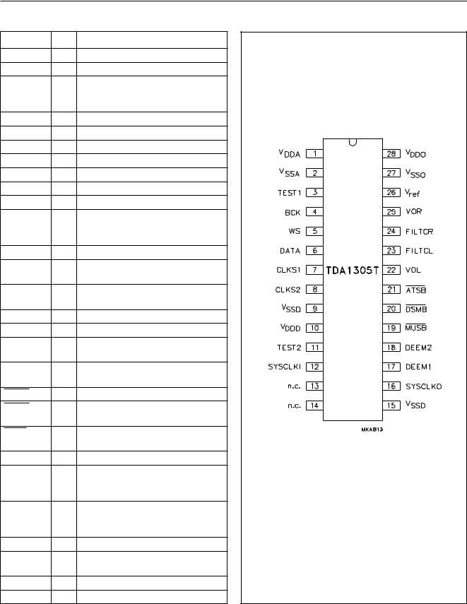
PINNING |
|
|
|
|
SYMBOL |
PIN |
DESCRIPTION |
|
|
VDDA |
1 |
analog supply voltage |
|
|
VSSA |
2 |
analog ground |
|
|
TEST1 |
3 |
test input; pin should be connected |
|
|
|
|
to ground (internal pull-down |
|
|
|
|
resistor) |
|
|
BCK |
4 |
bit clock input |
|
|
WS |
5 |
word select input |
|
|
DATA |
6 |
data input |
|
|
CLKS1 |
7 |
clock selection 1 input |
|
|
CLKS2 |
8 |
clock selection 2 input |
|
|
VSSD |
9 |
digital ground |
|
|
VDDD |
10 |
digital supply voltage |
|
|
TEST2 |
11 |
test input; pin should be connected |
|
|
|
|
to ground (internal pull-down |
|
|
|
|
resistor) |
|
|
SYSCLKI |
12 |
system clock input |
|
|
n.c. |
13 |
not connected (this pin should be left |
|
|
|
|
open-circuit) |
|
|
n.c. |
14 |
not connected (this pin should be left |
|
|
|
|
open-circuit) |
|
|
VSSD |
15 |
digital ground |
|
|
SYSCLKO |
16 |
system clock output |
|
|
DEEM1 |
17 |
de-emphasis on/off; fDEEM 32 kHz, |
|
|
|
|
44 kHz and 48 kHz |
|
|
DEEM2 |
18 |
de-emphasis on/off; fDEEM 32 kHz, |
|
|
|
|
44 kHz and 48 kHz |
|
|
MUSB |
19 |
mute input (active LOW) |
|
|
DSMB |
20 |
double-speed mode input |
|
|
|
|
(active LOW) |
|
|
ATSB |
21 |
12 dB attenuation input |
|
|
|
|
(active LOW) |
|
|
VOL |
22 |
left channel output |
|
|
FILTCL |
23 |
capacitor for left channel 1st order |
|
|
|
|
filter function should be connected |
|
|
|
|
between pins 22 and 23 |
|
|
FILTCR |
24 |
capacitor for right channel 1st order |
|
|
|
|
filter function should be connected |
|
|
|
|
between pins 25 and 24 |
|
|
VOR |
25 |
right channel output |
|
|
Vref |
26 |
internal reference voltage for output |
|
|
|
|
channels (0.5VDD) |
|
|
VSSO |
27 |
operational amplifier ground |
Fig.2 Pin configuration. |
|
VDDO |
28 |
operational amplifier supply voltage |
||
|
1995 Dec 08 |
5 |

Philips Semiconductors |
Preliminary specification |
|
|
Stereo 1fs data input up-sampling filter with
TDA1305T
bitstream continuous dual DAC (BCC-DAC2)
FUNCTIONAL DESCRIPTION
The TDA1305T CMOS digital-to-analog bitstream converter incorporates an up-sampling filter and noise shaper which increase the oversampling rate of 1fs input
data to 96fs (fsys = 192fs) or 128fs (fsys = 256fs) in the normal speed mode. In the double speed mode the
oversample rate of 1fs input data is increased to 48fs (fsys = 384fs) or 64fs (fsys = 256fs). This oversampling, together with the 5-bit DAC, enables the filtering required for waveform smoothing and out-of-band noise reduction to be achieved by simple 1st order analog post filtering.
System clock and data input format
The TDA1305T accommodates slave mode only, this means that in all applications the system devices must
Table 1 Data input format and system clock.
provide a system clock of 256 or 384fs (fs = 32, 44.1 or 48 kHz). The system frequency is selectable by means of pin CLKS1 and pin CLKS2. The SYSCLKO output (pin 16) provides the system clock for external use.
The TDA1305T supports the following data input modes:
∙I2S-bus with data word lengths of up to 20 bits (at fsys = 256fs).
∙LSB fixed serial format with data word lengths of 16, 18
and 20 bits (at fsys = 384fs). As this format idles on the MSB it is necessary to know how many bits are being transmitted.
The input format is shown in Fig.3. Left and right data-channel words are time-multiplexed.
TEST1 |
CLKS1 |
CLKS2 |
DATA INPUT FORMAT |
SYSTEM |
DATA |
SYSCLKO |
||
CLOCK |
CLOCK(1) |
|||||||
|
|
|
|
|
||||
0 |
0 |
0 |
I2S up to 20 bits |
256f |
s |
>20 |
256f |
|
|
|
|
|
|
|
s |
||
0 |
0 |
1 |
LSB fixed 16 bits |
384fs |
24 |
384fs |
||
0 |
1 |
0 |
LSB fixed 18 bits |
384fs |
24 |
384fs |
||
0 |
1 |
1 |
LSB fixed 20 bits |
384fs |
24 |
384fs |
||
1 |
0 |
0 |
reserved |
− |
|
− |
− |
|
|
|
|
|
|
|
|
||
1 |
0 |
1 |
LSB fixed 16 bits |
384fs |
32 |
384fs |
||
1 |
1 |
0 |
LSB fixed 18 bits |
384fs |
32 |
384fs |
||
1 |
1 |
1 |
LSB fixed 20 bits |
384fs |
32 |
384fs |
||
Note
1. Number of clock pulses within half an audio sample.
1995 Dec 08 |
6 |
 Loading...