


 Loading...
INTEGRATED CIRCUITS
DATA SHEET
TDA5140A
Brushless DC motor drive circuit
Product specification |
April 1994 |
Supersedes data of March 1992 |
|
File under Integrated Circuits, IC02 |
|
Philips Semiconductors

Philips Semiconductors |
Product specification |
|
|
Brushless DC motor drive circuit |
TDA5140A |
|
|
|
|
FEATURES
∙Full-wave commutation (using push/pull drivers at the output stages) without position sensors
∙Built-in start-up circuitry
∙Three push-pull outputs:
–0.8 A output current (typ.)
–low saturation voltage
–built-in current limiter
∙Thermal protection
∙Flyback diodes
∙Tacho output without extra sensor
∙Position pulse stage for phase-locked-loop control
∙Transconductance amplifier for an external control transistor.
QUICK REFERENCE DATA
Measured over full voltage and temperature range.
APPLICATIONS
∙VCR
∙Laser beam printer
∙Fax machine
∙Blower
∙Automotive.
GENERAL DESCRIPTION
The TDA5140A is a bipolar integrated circuit used to drive 3-phase brushless DC motors in full-wave mode. The device is sensorless (saving of 3 hall-sensors) using the back-EMF sensing technique to sense the rotor position.
SYMBOL |
PARAMETER |
CONDITIONS |
MIN. |
TYP. |
MAX. |
UNIT |
|
|
|
|
|
|
|
VP |
supply voltage |
note 1 |
4 |
− |
18 |
V |
VVMOT |
input voltage to the output |
note 2 |
1.7 |
− |
16 |
V |
|
driver stages |
|
|
|
|
|
|
|
|
|
|
|
|
VDO |
drop-out output voltage |
IO = 100 mA |
− |
0.93 |
1.05 |
V |
ILIM |
current limiting |
VVMOT = 10 V; RO = 3.9 Ω |
0.7 |
0.8 |
1 |
A |
Notes
1.An unstabilized supply can be used.
2.VVMOT = VP; +AMP IN = −AMP IN = 0 V; all outputs IO = 0 mA.
ORDERING INFORMATION
EXTENDED TYPE NUMBER |
|
|
PACKAGE |
|
|
|
|
|
|
|
|
PINS |
PIN POSITION |
|
MATERIAL |
CODE |
|
|
|
||||
|
|
|
|
|
|
TDA5140A |
18 |
DIL |
|
plastic |
SOT102 |
|
|
|
|
|
|
TDA5140AT |
20 |
SOL |
|
plastic |
SOT163A |
|
|
|
|
|
|
April 1994 |
2 |

Philips Semiconductors |
Product specification |
|
|
Brushless DC motor drive circuit |
TDA5140A |
|
|
BLOCK DIAGRAM
Fig.1 |
Block diagram (SOT102; DIL18). |
April 1994 |
3 |

Philips Semiconductors |
|
|
Product specification |
|
|
|
|
|
|
Brushless DC motor drive circuit |
TDA5140A |
|||
|
|
|
|
|
PINNING |
|
|
|
|
|
|
|
|
|
SYMBOL |
PIN |
PIN |
DESCRIPTION |
|
DIL18 |
SO20 |
|
||
|
|
|
||
|
|
|
|
|
MOT1 |
1 |
1 |
driver output 1 |
|
|
|
|
|
|
TEST |
2 |
2 |
test input/output |
|
|
|
|
|
|
n.c. |
|
3 |
not connected |
|
|
|
|
|
|
MOT2 |
3 |
4 |
driver output 2 |
|
|
|
|
|
|
VMOT |
4 |
5 |
input voltage for the output driver stages |
|
|
|
|
|
|
PG IN |
5 |
6 |
position generator: input from the position detector sensor to the position |
|
|
|
|
detector stage (optional); only if an external position coil is used |
|
|
|
|
|
|
PG/FG |
6 |
7 |
position generator/frequency generator: output of the rotation speed and position |
|
|
|
|
detector stages (open collector digital output, negative-going edge is valid) |
|
|
|
|
|
|
GND2 |
7 |
8 |
ground supply return for control circuits |
|
|
|
|
|
|
VP |
8 |
9 |
positive supply voltage |
|
CAP-CD |
9 |
10 |
external capacitor connection for adaptive communication delay timing |
|
|
|
|
|
|
CAP-DC |
10 |
11 |
external capacitor connection for adaptive communication delay timing copy |
|
|
|
|
|
|
CAP-ST |
11 |
12 |
external capacitor connection for start-up oscillator |
|
|
|
|
|
|
CAP-TI |
12 |
13 |
external capacitor connection for timing |
|
|
|
|
|
|
+AMP IN |
13 |
14 |
non-inverting input of the transconductance amplifier |
|
|
|
|
|
|
−AMP IN |
14 |
15 |
inverting input of the transconductance amplifier |
|
|
|
|
|
|
AMP OUT |
15 |
16 |
transconductance amplifier output (open collector) |
|
|
|
|
|
|
MOT3 |
16 |
17 |
driver output 3 |
|
|
|
|
|
|
n.c. |
− |
18 |
not connected |
|
|
|
|
|
|
MOT0 |
17 |
19 |
input from the star point of the motor coils |
|
|
|
|
|
|
GND1 |
18 |
20 |
ground (0 V) motor supply return for output stages |
|
|
|
|
|
|
April 1994 |
4 |

Philips Semiconductors |
Product specification |
|
|
Brushless DC motor drive circuit |
TDA5140A |
|
|
Fig.2 Pin configuration (SOT102; DIL18).
FUNCTIONAL DESCRIPTION
The TDA5140A offers a sensorless three phase motor drive function. It is unique in its combination of sensorless motor drive and full-wave drive. The TDA5140A offers protected outputs capable of handling high currents and can be used with star or delta connected motors. It can easily be adapted for different motors and applications. The TDA5140A offers the following features:
∙Sensorless commutation by using the motor EMF.
∙Built-in start-up circuit.
∙Optimum commutation, independent of motor type or motor loading.
∙Built-in flyback diodes.
∙Three phase full-wave drive.
∙High output current (0.8 A).
∙Outputs protected by current limiting and thermal protection of each output transistor.
∙Low current consumption by adaptive base-drive.
∙Accurate frequency generator (FG) by using the motor EMF.
∙Amplifier for external position generator (PG) signal.
Fig.3 Pin configuration (SOT163A; SO20L).
∙Suitable for use with a wide tolerance, external PG sensor.
∙Built-in multiplexer that combines the internal FG and external PG signals on one pin for easy use with a controlling microprocessor.
∙Uncommitted operational transconductance amplifier (OTA), with a high output current, for use as a control amplifier.
April 1994 |
5 |
Philips Semiconductors |
|
|
|
|
|
|
|
|
|
|
|
|
|
|
|
|
|
|
|
|
|
|
|
|
|
|
Product specification |
|||||||||||||||
|
|
|
|
|
|
|
|
|
|
|
|
|
|
|
|
|
|
|
|
|
|
|
|
|
|
|
|
|
|
|
|
|
|
|
|
|
||||||
Brushless DC motor drive circuit |
|
|
|
|
|
|
|
|
|
|
|
|
|
|
|
|
|
TDA5140A |
||||||||||||||||||||||||
|
|
|
|
|
|
|
|
|
|
|
|
|
|
|
|
|
|
|
|
|
|
|
|
|
|
|
|
|
|
|
|
|
|
|
|
|
|
|
|
|
|
|
LIMITING VALUES |
|
|
|
|
|
|
|
|
|
|
|
|
|
|
|
|
|
|
|
|
|
|
|
|
|
|
|
|
|
|
|
|
|
|
|
|
||||||
In accordance with the Absolute Maximum Rating System (IEC 134). |
|
|
|
|
|
|
|
|
|
|
|
|
|
|
|
|
|
|||||||||||||||||||||||||
|
|
|
|
|
|
|
|
|
|
|
|
|
|
|
|
|
|
|
|
|
|
|
|
|
|
|
|
|
|
|
|
|
|
|
|
|
|
|
|
|||
SYMBOL |
|
|
|
|
|
PARAMETER |
|
|
CONDITIONS |
|
|
MIN. |
|
|
|
|
MAX. |
|
|
UNIT |
||||||||||||||||||||||
|
|
|
|
|
|
|
|
|
|
|
|
|
|
|
|
|
|
|
|
|
|
|
|
|
|
|
|
|
|
|
|
|
|
|
|
|
|
|
|
|||
VP |
supply voltage |
|
|
|
|
|
|
|
|
|
|
|
|
− |
|
|
18 |
|
|
|
|
|
|
|
V |
|||||||||||||||||
VI |
input voltage; all pins except |
|
|
VI < 18 V |
|
−0.3 |
|
|
VP + 0.5 |
|
|
|
|
|
V |
|||||||||||||||||||||||||||
|
|
|
|
|
VMOT |
|
|
|
|
|
|
|
|
|
|
|
|
|
|
|
|
|
|
|
|
|
|
|
|
|
|
|
|
|
|
|
|
|
||||
|
|
|
|
|
|
|
|
|
|
|
|
|
|
|
|
|
|
|
|
|
|
|
|
|
|
|
|
|
|
|
|
|
|
|
|
|
|
|
|
|||
VVMOT |
VMOT input voltage |
|
|
|
|
|
|
|
|
|
|
|
|
−0.5 |
|
|
17 |
|
|
|
|
|
|
|
V |
|||||||||||||||||
VO |
output voltage |
|
|
|
|
|
|
|
|
|
|
|
|
|
|
|
|
|
|
|
|
|
|
|
|
|
|
|
|
|
|
|
||||||||||
|
|
|
|
|
|
|
AMP OUT and PG/FG |
|
|
|
|
|
|
|
|
|
GND |
|
|
VP |
|
|
|
|
|
|
|
V |
||||||||||||||
|
|
|
|
|
|
|
MOT1, MOT2 and MOT3 |
|
|
|
|
|
|
|
|
|
−1 |
|
|
VVMOT + VDHF |
|
|
V |
|||||||||||||||||||
VI |
input voltage CAP-ST, CAP-TI, |
|
|
|
|
|
|
|
− |
|
|
2.5 |
|
|
|
|
|
|
|
V |
||||||||||||||||||||||
|
|
|
|
|
CAP-CD and CAP-DC |
|
|
|
|
|
|
|
|
|
|
|
|
|
|
|
|
|
|
|
|
|
|
|
|
|
||||||||||||
|
|
|
|
|
|
|
|
|
|
|
|
|
|
|
|
|
|
|
|
|
|
|
|
|
|
|
|
|
|
|
|
|
|
|
|
|
|
|
||||
Tstg |
storage temperature |
|
|
|
|
|
|
|
|
|
|
|
|
−55 |
|
|
+150 |
|
|
|
|
|
|
°C |
||||||||||||||||||
Tamb |
operating ambient temperature |
|
|
|
|
|
|
0 |
|
|
|
|
+70 |
|
|
|
|
|
|
|
°C |
|||||||||||||||||||||
Ptot |
total power dissipation |
|
|
see Figs 4 and 5 |
|
− |
|
|
− |
|
|
|
|
|
|
|
W |
|||||||||||||||||||||||||
Ves |
electrostatic handling |
|
|
|
|
|
see “Handling” |
|
− |
|
|
500 |
|
|
|
|
|
|
|
V |
||||||||||||||||||||||
|
|
|
|
|
|
|
|
|
|
|
|
|
|
|
|
|
|
|
|
|
|
|
|
|
|
|
|
|
|
|
|
|
|
|
|
|
|
|
||||
3 |
|
|
|
|
|
|
|
|
|
|
|
|
|
|
MBD535 |
3 |
|
|
|
|
|
|
|
|
|
|
|
|
|
|
|
MBD536 |
||||||||||
|
|
|
|
|
|
|
|
|
|
|
|
|
|
|
|
|
|
|
|
|
|
|
|
|
|
|
|
|
|
|
|
|
|
|
|
|
||||||
|
|
|
|
|
|
|
|
|
|
|
|
|
|
|
|
|
|
|
|
|
|
|
|
|
|
|
|
|
|
|
|
|
|
|
|
|||||||
P tot |
|
|
|
|
|
|
|
|
|
|
|
|
|
|
|
|
|
|
|
P tot |
|
|
|
|
|
|
|
|
|
|
|
|
|
|
|
|
|
|
||||
(W) |
|
|
|
|
|
|
|
|
|
|
|
|
|
|
|
|
|
|
|
(W) |
|
|
|
|
|
|
|
|
|
|
|
|
|
|
|
|
|
|
||||
2.28 |
|
|
|
|
|
|
|
|
|
|
|
|
|
|
|
|
|
|
2 |
|
|
|
|
|
|
|
|
|
|
|
|
|
|
|
|
|
|
|
||||
|
|
|
|
|
|
|
|
|
|
|
|
|
|
|
|
|
|
|
|
|
|
|
|
|
|
|
|
|
|
|
|
|
|
|
|
|
||||||
2 |
|
|
|
|
|
|
|
|
|
|
|
|
|
|
|
|
|
|
|
|
|
|
|
|
|
|
|
|
|
|
|
|
|
|
|
|
|
|||||
|
|
|
|
|
|
|
|
|
|
|
|
|
|
|
|
|
|
|
|
|
|
|
|
|
|
|
|
|
|
|
|
|
|
|
|
|||||||
1.05 |
|
|
|
|
|
|
|
|
|
|
|
|
|
|
|
|
|
|
1.38 |
|
|
|
|
|
|
|
|
|
|
|
|
|
|
|
|
|
|
|
||||
|
|
|
|
|
|
|
|
|
|
|
|
|
|
|
|
|
|
|
|
|
|
|
|
|
|
|
|
|
|
|
|
|
|
|
|
|
||||||
|
|
|
|
|
|
|
|
|
|
|
|
|
|
|
|
|
|
|
|
|
|
|
|
|
|
|
|
|
|
|
|
|
|
|
|
|
||||||
|
|
|
|
|
|
|
|
|
|
|
|
|
|
|
|
|
|
1 |
|
|
|
|
|
|
|
|
|
|
|
|
|
|
|
|
|
|
|
|||||
|
|
|
|
|
|
|
|
|
|
|
|
|
|
|
|
|
|
|
|
|
|
|
|
|
|
|
|
|
|
|
|
|
|
|
|
|
|
|
||||
0 |
|
|
|
|
|
|
|
|
|
|
|
|
|
|
|
|
|
|
0 |
|
|
|
|
|
|
|
|
|
|
|
|
|
|
|
|
|
|
|
||||
|
|
|
|
|
|
|
|
|
|
|
|
|
|
|
|
|
|
|
|
|
|
|
|
|
|
|
|
|
|
|
|
|
|
|
|
|
||||||
50 |
|
0 |
50 |
70 |
100 |
|
150 |
|
200 |
50 |
0 |
|
50 |
70 |
100 |
150 |
200 |
|||||||||||||||||||||||||
|
|
|
|
|
|
|
|
|
||||||||||||||||||||||||||||||||||
|
|
|
|
|
|
|
||||||||||||||||||||||||||||||||||||
|
|
|
|
|
|
|
|
|
|
|
|
|
|
Tamb (oC) |
|
|
|
|
|
|
|
|
|
|
|
|
|
|
|
|
|
|
|
Tamb (oC) |
||||||||
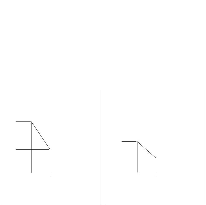
Fig.4 Power derating curve (SOT102; DIL18).
Fig.5 Power derating curve (SOT163A; SO20L).
HANDLING
Every pin withstands the ESD test in accordance with “MIL-STD-883C class 2”. Method 3015 (HBM 1500 Ω, 100 pF) 3 pulses + and 3 pulses − on each pin referenced to ground.
April 1994 |
6 |

Philips Semiconductors |
|
|
|
Product specification |
||||
|
|
|
|
|
|
|
|
|
Brushless DC motor drive circuit |
|
|
|
|
TDA5140A |
|||
|
|
|
|
|
|
|
|
|
CHARACTERISTICS |
|
|
|
|
|
|
||
VP = 14.5 V; Tamb = 25 °C; unless otherwise specified. |
|
|
|
|
|
|||
|
|
|
|
|
|
|
|
|
SYMBOL |
PARAMETER |
|
CONDITIONS |
MIN. |
TYP. |
|
MAX. |
UNIT |
|
|
|
|
|
|
|
|
|
Supply |
|
|
|
|
|
|
|
|
|
|
|
|
|
|
|
|
|
VP |
supply voltage |
|
note 1 |
4 |
− |
|
18 |
V |
IP |
supply current |
|
note 2 |
− |
3.7 |
|
5 |
mA |
VVMOT |
input voltage to the output driver |
|
see Fig.1 |
1.7 |
− |
|
16 |
V |
|
stages |
|
|
|
|
|
|
|
|
|
|
|
|
|
|
|
|
Thermal protection |
|
|
|
|
|
|
||
|
|
|
|
|
|
|
|
|
TSD |
local temperature at |
|
|
130 |
140 |
|
150 |
°C |
|
temperature sensor causing |
|
|
|
|
|
|
|
|
shut-down |
|
|
|
|
|
|
|
|
|
|
|
|
|
|
|
|
T |
reduction in temperature before |
|
after shut-down |
− |
TSD − 30 |
|
− |
K |
|
switch-on |
|
|
|
|
|
|
|
|
|
|
|
|
|
|
|
|
MOT0; centre tap |
|
|
|
|
|
|
||
|
|
|
|
|
|
|
|
|
VI |
input voltage |
|
|
−0.5 |
− |
|
VVMOT |
V |
II |
input bias current |
|
0.5 V < VI < VVMOT − 1.5 V |
−10 |
− |
|
0 |
μA |
VCSW |
comparator switching level |
|
note 3 |
±20 |
±30 |
|
±40 |
mV |
VCSW |
variation in comparator |
|
|
−3 |
0 |
|
+3 |
mV |
|
switching levels |
|
|
|
|
|
|
|
|
|
|
|
|
|
|
|
|
Vhys |
comparator input hysteresis |
|
|
− |
75 |
|
− |
μV |
MOT1, MOT2 and MOT3 |
|
|
|
|
|
|
||
|
|
|
|
|
|
|
|
|
VDO |
drop-out output voltage |
|
IO = 100 mA |
− |
0.93 |
|
1.05 |
V |
|
|
|
IO = 500 mA |
− |
1.65 |
|
1.80 |
V |
VOL |
variation in saturation voltage |
|
IO = 100 mA |
− |
− |
|
180 |
mV |
|
between lower transistors |
|
|
|
|
|
|
|
|
|
|
|
|
|
|
|
|
VOH |
variation in saturation voltage |
|
IO = −100 mA |
− |
− |
|
180 |
mV |
|
between upper transistors |
|
|
|
|
|
|
|
|
|
|
|
|
|
|
|
|
ILIM |
current limiting |
|
VVMOT = 10 V; RO = 6.8 Ω |
0.7 |
0.8 |
|
1 |
A |
VDHF |
diode forward voltage (diode DH) |
|
IO = −500 mA; notes 4 |
− |
− |
|
1.5 |
V |
|
|
|
and 5; see Fig.1 |
|
|
|
|
|
|
|
|
|
|
|
|
|
|
VDLF |
diode forward voltage (diode DL) |
|
IO = 500 mA; notes 4 and |
−1.5 |
− |
|
− |
V |
|
|
|
5; see Fig.1 |
|
|
|
|
|
|
|
|
|
|
|
|
|
|
IDM |
peak diode current |
|
note 5 |
− |
− |
|
1 |
A |
+AMP IN and −AMP IN |
|
|
|
|
|
|
||
|
|
|
|
|
|
|
|
|
VI |
input voltage |
|
|
−0.3 |
− |
|
VP − 1.7 |
V |
|
differential mode voltage without |
|
|
− |
− |
|
±VP |
V |
|
'latch-up' |
|
|
|
|
|
|
|
|
|
|
|
|
|
|
|
|
Ib |
input bias current |
|
|
− |
− |
|
650 |
nA |
CI |
input capacitance |
|
|
− |
4 |
|
− |
pF |
Voffset |
input offset voltage |
|
|
− |
− |
|
10 |
mV |
April 1994 |
7 |

Philips Semiconductors |
|
|
|
Product specification |
||||
|
|
|
|
|
|
|
|
|
Brushless DC motor drive circuit |
|
|
|
|
TDA5140A |
|||
|
|
|
|
|
|
|
|
|
|
|
|
|
|
|
|
|
|
SYMBOL |
PARAMETER |
|
CONDITIONS |
MIN. |
TYP. |
|
MAX. |
UNIT |
|
|
|
|
|
|
|
|
|
AMP OUT (open collector) |
|
|
|
|
|
|
||
|
|
|
|
|
|
|
|
|
II |
output sink current |
|
|
40 |
− |
|
− |
mA |
Vsat |
saturation voltage |
|
II = 40 mA |
− |
1.5 |
|
2.1 |
V |
VO |
output voltage |
|
|
−0.5 |
− |
|
+18 |
V |
SR |
slew rate |
|
RL = 330 Ω; CL = 50 pF |
− |
60 |
|
− |
mA/μs |
Gtr |
transfer gain |
|
|
0.3 |
− |
|
− |
S |
PG IN |
|
|
|
|
|
|
|
|
|
|
|
|
|
|
|
|
|
VI |
input voltage |
|
|
−0.3 |
− |
|
+5 |
V |
Ib |
input bias current |
|
|
− |
− |
|
650 |
nA |
RI |
input resistance |
|
|
5 |
− |
|
30 |
kΩ |
VCWS |
comparator switching level |
|
|
86 |
− |
|
107 |
mV |
Vhys |
comparator input hysteresis |
|
|
− |
±8 |
|
− |
mV |
PG/FG (open collector) |
|
|
|
|
|
|
||
|
|
|
|
|
|
|
|
|
VOL |
LOW level output voltage |
|
IO = 1.6 mA |
− |
− |
|
0.4 |
V |
VOH(max) |
maximum HIGH level output |
|
|
VP |
− |
|
− |
V |
|
voltage |
|
|
|
|
|
|
|
|
|
|
|
|
|
|
|
|
tTHL |
HIGH-to-LOW transition time |
|
CL = 50 pF; RL = 10 kΩ |
− |
0.5 |
|
− |
μs |
|
ratio of PG/FG frequency and |
|
|
− |
1 : 2 |
|
− |
|
|
commutation frequency |
|
|
|
|
|
|
|
|
|
|
|
|
|
|
|
|
δ |
duty factor |
|
|
− |
50 |
|
− |
% |
|
|
|
|
|
|
|
|
|
tPL |
pulse width LOW |
|
after a PG IN pulse |
5 |
7 |
|
18 |
μs |
CAP-ST |
|
|
|
|
|
|
|
|
|
|
|
|
|
|
|
|
|
Isink |
output sink current |
|
|
1.5 |
2.0 |
|
2.5 |
μA |
Isource |
output source current |
|
|
−2.5 |
−2.0 |
|
−1.5 |
μA |
VSWL |
LOW level switching voltage |
|
|
− |
0.20 |
|
− |
V |
VSWH |
HIGH level switching voltage |
|
|
− |
2.20 |
|
− |
V |
CAP-TI |
|
|
|
|
|
|
|
|
|
|
|
|
|
|
|
|
|
Isink |
output sink current |
|
|
− |
28 |
|
− |
μA |
Isource |
output source current |
|
0.05 V < VCAP-TI < 0.3 V |
− |
−57 |
|
− |
μA |
|
|
|
0.3 V < VCAP-TI < 2.2 V |
− |
−5 |
|
− |
μA |
VSWL |
LOW level switching voltage |
|
|
− |
50 |
|
− |
mV |
VSWM |
MIDDLE level switching voltage |
|
|
− |
0.30 |
|
− |
V |
VSWH |
HIGH level switching voltage |
|
|
− |
2.20 |
|
− |
V |
April 1994 |
8 |
Loading...