


INTEGRATED CIRCUITS
TDA4780
RGB video processor with automatic cut-off control and gamma adjust
Preliminary specification |
|
May 1994 |
|||||
File under Integrated Circuits, IC02 |
|
|
|
|
|
|
|
|
|
|
|
|
|
|
|
|
|
|
|
|
|
|
|
|
|
|
|
|
|
|
|

Philips Semiconductors |
Preliminary specification |
|
|
RGB video processor with automatic
TDA4780
cut-off control and gamma adjust
FEATURES
∙Gamma adjust
∙Dynamic black control (adaptive black)
∙All input signals clamped on black-levels
∙Automatic cut-off control, alternative: output clamping on fixed levels
∙Three adjustable reference voltage levels via I2C-bus for automatic cut-off control
∙Luminance/colour difference interface
∙Two luminance input levels allowed
∙Two RGB interfaces controlled by either fast switches or by I2C-bus
∙Two peak drive limiters, selection via I2C-bus
∙Blue stretch, selection via I2C-bus
∙Luminance output for scan velocity modulation (SCAVEM)
∙Extra luminance output; same pin can be used as hue control output e.g. for the TDA4650 and TDA4655
∙Non standard operations like 50 Hz/32 kHz are also possible
∙Either 2 or 3 level sandcastle pulse applicable
∙High bandwidth for 32 kHz application
∙White point adjusts via I2C-bus
∙Average beam current and improved peak drive limiting
∙Two switch-on delays to prevent discolouration during start-up
∙All functions and features programmable via I2C-bus
∙PAL/SECAM or NTSC matrix selection.
GENERAL DESCRIPTION
The TDA4780 is a monolithic integrated circuit with a luminance and a colour difference interface for video processing in TV receivers. Its primary function is to process the luminance and colour difference signals from a colour decoder which is equipped e.g. with the multistandard decoder TDA4655 or TDA9160 plus delay line TDA4661 or TDA4665 and the Picture Signal Improvement (PSI) IC TDA467x or from a Feature Module.
(continued)
QUICK REFERENCE DATA
SYMBOL |
PARAMETER |
MIN. |
TYP. |
MAX. |
UNIT |
|
|
|
|
|
|
VP |
supply voltage (pin 5) |
7.2 |
8.0 |
8.8 |
V |
IP |
supply current (pin 5) |
80 |
100 |
120 |
mA |
V8(p-p) |
luminance input (peak-to-peak value) (C)VBS |
− |
0.45/ 1.43 |
− |
V |
V6(p-p) |
−(B−Y) input (peak-to-peak value) |
− |
1.33 |
− |
V |
V7(p-p) |
−(R−Y) input (peak-to-peak value) |
− |
1.05 |
− |
V |
V14 |
three-level sandcastle pulse |
|
|
|
|
|
H+V |
− |
2.5 |
− |
V |
|
H |
− |
4.5 |
− |
V |
|
BK |
− |
8.0 |
− |
V |
|
|
|
|
|
|
|
two-level sandcastle pulse |
|
|
|
|
|
H+V |
− |
2.5 |
− |
V |
|
BK |
− |
4.5 |
− |
V |
|
|
|
|
|
|
Vi |
RGB input signals at pins 2, 3, 4, 10, 11 and 12 (black-to-white value) |
− |
0.7 |
− |
V |
VO(p-p) |
RGB output at pins 24, 22 and 20 (black-to-white value) |
− |
2.0 |
− |
V |
Tamb |
operating ambient temperature |
−20 |
− |
+70 |
°C |
May 1994 |
2 |

Philips Semiconductors |
Preliminary specification |
|
|
RGB video processor with automatic
TDA4780
cut-off control and gamma adjust
ORDERING INFORMATION
EXTENDED |
|
|
PACKAGE |
|
|
|
|
|
|
||
|
PIN |
|
|
||
TYPE NUMBER |
PINS |
MATERIAL |
CODE |
||
POSITION |
|||||
|
|||||
|
|
|
|
||
|
|
|
|
|
|
TDA4780 |
28 |
DIL |
plastic |
SOT117(1) |
Note
1. SOT117-1; 1996 December 9.
May 1994 |
3 |

Philips Semiconductors |
Preliminary specification |
|
|
RGB video processor with automatic
TDA4780
cut-off control and gamma adjust
Fig.1 Block diagram (continued in Fig.2)
May 1994 |
4 |

Philips Semiconductors |
Preliminary specification |
|
|
RGB video processor with automatic
TDA4780
cut-off control and gamma adjust
Fig.2 Block diagram (continued from Fig.1)
May 1994 |
5 |
Philips Semiconductors |
Preliminary specification |
|
|
RGB video processor with automatic
TDA4780
cut-off control and gamma adjust
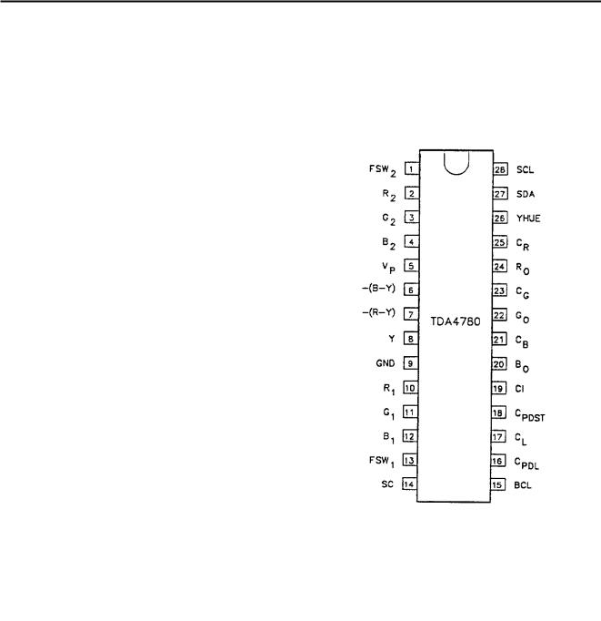
PINNING |
|
|
|
|
|
|
|
|
|
||
|
|
|
|
|
|
SYMBOL |
PIN |
DESCRIPTION |
|
|
|
|
|
|
|
|
|
FSW2 |
1 |
fast switch 2 input |
|
|
|
R2 |
2 |
red input 2 |
|
|
|
G2 |
3 |
green input 2 |
|
|
|
B2 |
4 |
blue input 2 |
|
|
|
VP |
5 |
supply voltage |
|
|
|
−(B−Y) |
6 |
colour difference input −(B−Y) |
|
|
|
|
|
|
|
|
|
−(R−Y) |
7 |
colour difference input −(R−Y) |
|
|
|
|
|
|
|
|
|
Y |
8 |
luminance input |
|
|
|
|
|
|
|
|
|
GND |
9 |
ground |
|
|
|
|
|
|
|
|
|
R1 |
10 |
red input 1 |
|
|
|
G1 |
11 |
green input 1 |
|
|
|
B1 |
12 |
blue input 1 |
|
|
|
FSW1 |
13 |
fast switch 1 input |
|
|
|
SC |
14 |
sandcastle pulse input |
|
|
|
|
|
|
|
|
|
BCL |
15 |
average beam current limiting |
|
|
|
|
|
input |
|
|
|
|
|
|
|
|
|
CPDL |
16 |
storage capacitor for peak |
|
|
|
|
|
limiting |
|
|
|
|
|
|
|
|
|
CL |
17 |
storage capacitor for leakage |
|
|
|
|
|
current compensation |
|
|
|
|
|
|
|
|
|
CPDST |
18 |
storage capacitor for peak dark |
|
|
|
CI |
19 |
cut-off measurement input |
|
|
|
|
|
|
|
|
|
BO |
20 |
blue output |
|
|
|
CB |
21 |
blue cut-off storage capacitor |
|
|
|
GO |
22 |
green output |
|
|
|
CG |
23 |
green cut-off storage capacitor |
|
|
|
RO |
24 |
red output |
|
|
|
CR |
25 |
red cut-off storage capacitor |
|
|
|
YHUE |
26 |
Y-output/hue adjust output |
|
|
|
|
|
|
|
|
|
SDA |
27 |
I2C-bus serial data |
|
|
|
|
|
input/acknowledge output |
|
Fig.3 Pin configuration. |
|
|
|
|
|
||
SCL |
28 |
I2C-bus serial clock input |
|||
|
|
||||
|
|
|
|
|
May 1994 |
6 |

Philips Semiconductors |
Preliminary specification |
|
|
RGB video processor with automatic
TDA4780
cut-off control and gamma adjust
GENERAL DESCRIPTION
(continued)
The required input signals are:
∙luminance and negative colour difference signals
∙2- or 3-level sandcastle pulse for internal timing pulse generation
∙I2C-bus data and clock signals
Two sets of analog RGB colour signals can also be inserted, e.g. one from a peritelevision connector (SCART plug) and the other one from an on-screen display (OSD) generator. The TDA4780 has I2C-bus control of all parameters and functions with automatic cut-off control of the picture tube cathode currents. It provides RGB output signals for the video output stages. In clamped output mode it can also be used as an RGB source.
The main differences to the sister type TDA4680 are:
∙additional features, namely gamma adjust, adaptive black, blue stretch and two different peak drive limiters.
∙the measurement lines are triggered by the trailing edge of the vertical component of the sandcastle pulse.
∙I2C-bus receiver only. Automatic white level control is not provided; the white levels are determined directly by the I2C-bus data.
∙the TDA4780 is pin compatible (except pin 18) to the TDA4680. The slave address via the I2C-bus can be used for both ICs; where a function is not included in the TDA4680 then the I2C-bus command is not executed. Special commands (except control bit FSWL) for the TDA4680 will be ignored by the TDA4780.
FUNCTIONAL DESCRIPTION
Signal input stages
The TDA4780 contains 3 sets of input signal stages for:
a)Luminance/colour-difference signals: (Y: 0.45 V(p-p) VBS or 1.43 V(p-p) VBS, selectable via I2C-bus, −(R−Y): 1.05 V(p-p); −(B−Y): 1.33 V(p-p)). The capacitively coupled signals are matrixed to RGB signals by either a PAL/SECAM or NTSC matrix (selected via I2C-bus).
b)(RGB)1 signals (0.7 V(p-p) VB), capacitively coupled (e.g. from external source).
c)(RGB)2 signals (0.7 V(p-p) VB), capacitively coupled (e.g. videotext, OSD).
All input signals are clamped in order to have the same black levels at the signal switch input. Displayed signals must be synchronous with the sandcastle pulse.
Signal switches
Both fast signal switches can be operated by switching pins (e.g. SCART facilities) or set via the I2C-bus. By switch 1 the Y-CD signals or the (RGB)1 signals can be selected, by switch 2 the above selected signals or the (RGB)2 signals are enabled. During the vertical and horizontal blanking time an artificial black level equal to the clamped black level is inserted in order to clip off the sync pulse of the luminance signal and to suppress hum during the cut-off measurement time and eliminate noise during these intervals.
Saturation, gamma, contrast and brightness adjust
Saturation, contrast and brightness adjusts are adjusted via the I2C-bus and act on Y, CD as well as on RGB input signals. Gamma acts on the luminance content of the input signals.
Gamma adjust
The gamma adjust stage has a non-linear transmission characteristic according to the formula y = xgamma, where x represents the input and y the output signal. If gamma is smaller than unity, the lower parts of the signal are amplified with higher gain.
Adaptive black (ADBL)
The adaptive black stage detects the lowest voltage of the luminance component of the internal RGB signals during the scanning time and shifts it to the nominal black level. In order to keep the nominal white level the contrast is increased simultaneously.
May 1994 |
7 |

Philips Semiconductors |
Preliminary specification |
|
|
RGB video processor with automatic
TDA4780
cut-off control and gamma adjust
Blue stretch (BLST)
The blue stretch channel gets additional amplification if the blue signal is greater than 80% of the nominal signal amplitude. In that case the white point is shifted towards higher colour temperature so that white parts of a picture seem to be brighter.
Measurement pulse and blanking stage
During the vertical and horizontal blanking time and the measurement period the signals are blanked to an ultra black level, so the leakage current of the picture tube can be measured and automatically compensated for. During the cut-off measurement lines (one line period for each R, G or B) the output signal levels are at cut-off measurement level.
The vertical blanking period is timed by the sandcastle pulse. The measurement pulses (leakage, R, G and B) are triggered by the negative going edge of the vertical pulse of the sandcastle pulse and start after the following horizontal pulse.
The IC is prepared for 2fH (32 kHz) application.
Output amplifier and white adjust potentiometer
The RGB signals are amplified to nominal 2 V(p-p), the DC-levels are shifted according to cut-off control.
The nominal signal amplitude can be varied by ±50% by the white point adjustment via the I2C-bus (individually for RGB respect).
Automatic cut-off control
During leakage measurement time the leakage current is compensated in order to get a reference voltage at the cut-off measurement info pin.
This compensation value is stored in an external capacitor. During cut-off current measurement times for the R, G and B channels, the voltage at this pin is compared with the reference voltage, which is individually adjustable via I2C-bus for each colour channel. The so derived control voltages are stored in the external feedback capacitors. Shift stages add these voltages to the corresponding output signals.
The automatic cut-off control may be disabled via the I2C-bus. In this mode the output voltage is clamped to 2.5 V. Clamping periods are the same as the cut-off measurement periods.
Signal limiting
The TDA4780 provides two kinds of signal limiting. First, an average beam limiting, that reduces signal level if a certain average is exceeded. Second, a peak drive
limiting, that is activated if one of the RGB signals even shortly exceeds a via I2C-bus adjusted threshold. The latter can be either referred to the cut-off measurement level of the outputs or to ground.
When signal limiting occurs, contrast is reduced, and at minimum contrast brightness is reduced additionally.
Sandcastle decoder and timer
A 3-level detector separates the sandcastle pulse into combined line and field pulses, line pulses, and clamping pulses. The timer contains a line counter and controls the cut-off control measurement. Application with a 2-level 5 V sandcastle pulse is possible.
Switch on delay circuit
After switch on all signals are blanked and a warm up test pulse is fed to the outputs during the cut-off measurement lines. If the voltage at the cut-off measurement input exceeds an internal level the cut-off control is enabled but the signal remains still blanked. The signal blanking is finished when the cut-off control has stabilized. In case of output clamping, the cut-off control is disabled and the switch on procedure will be skipped.
Y output and hue adjust
The TDA4780 contains a D/A converter for hue adjust. The analog information can be fed, e.g. to the multistandard decoder TDA4650 or TDA4655. This output pin may be switched to a Y output signal, which can be used for scan velocity modulation (SCAVEM). The Y output is the Y input signal or the matrixed (RGB) input signal according to the switch position of fast switch.
I2C-bus
The TDA4780 contains an I2C-bus receiver for control function.
ESD protection
Pins are provided with protection diodes against ground and supply voltage (see pin description).
I2C-bus input pins do not shunt the I2C-bus signals in case of missing supply voltage.
EMC
Pins are protected against electromagnetic radiation.
May 1994 |
8 |

Philips Semiconductors |
Preliminary specification |
|
|
RGB video processor with automatic
TDA4780
cut-off control and gamma adjust
LIMITING VALUES
In accordance with the Absolute Maximum Rating System (IEC 134).
SYMBOL |
PARAMETER |
MIN. |
MAX. |
UNIT |
|
|
|
|
|
|
|
Tstg |
storage temperature |
−20 |
+150 |
°C |
|
Tamb |
operating ambient temperature |
−20 |
+70 |
°C |
|
Ptot |
total power dissipation |
− |
1200 |
mW |
|
V5-9 = VP |
supply voltage |
−0.1 |
+9.0 |
V |
|
V10,11,12-9 |
(RGB)1 inputs |
−0.1 |
VP |
V |
|
V2,3,4-9 |
(RGB)2 inputs |
−0.1 |
VP |
V |
|
V8,7,6-9 |
Y, CD-inputs |
−0.1 |
VP |
V |
|
V13,1-9 |
switch I, II |
−0.1 |
VP |
V |
|
V25,23,21,17-9 |
black level, leakage storage |
−0.1 |
VP |
V |
|
V14-9 |
sandcastle |
−0.7 |
VP + 5.8 |
V |
|
V15-9 |
average current inf. |
−0.7 |
VP + 0.7 |
V |
|
V16-9 |
peak drive storage |
−0.1 |
VP |
V |
|
V |
I2C-bus |
−0.1 |
V |
P |
V |
27,28-9 |
|
|
|
|
|
I26 |
Y output / hue adjust |
−8 |
− |
|
mA |
V18-9 |
peak dark storage |
−0.1 |
VP |
V |
|
V19-9 |
cut-off control input |
−0.7 |
VP + 0.7 |
V |
|
I24,22,20 |
output peak |
−20 |
− |
|
mA |
I24,22,20 |
output average |
−10 |
− |
|
mA |
ESD |
electrostatic handling (note 1) for all pins |
−500 |
+500 |
V |
|
|
|
|
|
|
|
Note to the Limiting Values
1. Charge device model class A: discharging a 200 pF capacitor through a 0 Ω series resistor.
THERMAL RESISTANCE
SYMBOL |
PARAMETER |
THERMAL RESISTANCE |
|
|
|
Rth j-a |
from junction to ambient in free air |
47 K/W |
QUALITY SPECIFICATION
URV-4-2-59/601
May 1994 |
9 |

Philips Semiconductors |
Preliminary specification |
|
|
RGB video processor with automatic
TDA4780
cut-off control and gamma adjust
CHARACTERISTICS
Tamb = +25 °C; VP = 8 V; Vnom: nominal signal amplitude (black-white) 2000 mV (peak-to-peak value) at output pins; gamma = 1; adaptive black inactive; brightness, contrast, saturation and white balance at nominal settings; no beam current or peak drive limiting; all voltages are related to ground (pin 9) and measured in Figs 1 and 2; unless otherwise specified.
SYMBOL |
PARAMETER |
CONDITIONS |
MIN. |
TYP. |
|
MAX. |
UNIT |
|
|
|
|
|
|
|
|
VP |
supply voltage (pin 5) |
|
7.2 |
8 |
|
8.8 |
V |
IP |
supply current (pin 5) |
|
− |
100 |
|
120 |
mA |
Colour-difference inputs (−(B−Y): pin 6, −(R−Y): pin 7; capacitively coupled to a low ohmic source; |
|
||||||
recommendation: maximum 600 Ω) |
|
|
|
|
|
|
|
|
|
|
|
|
|
|
|
V6 |
−(B−Y) signal (peak-to-peak |
75% colour bar signal |
− |
1.33 |
|
− |
V |
|
value) |
|
|
|
|
|
|
|
|
|
|
|
|
|
|
V6,7 |
internal bias during clamping |
|
− |
4.0 |
|
− |
V |
I6,7 |
DC input current between |
|
− |
− |
|
0.1 |
μA |
|
clamping pulses |
|
|
|
|
|
|
|
|
|
|
|
|
|
|
I6,7 |
maximum input current during |
|
100 |
180 |
|
260 |
μA |
|
clamping |
|
|
|
|
|
|
|
|
|
|
|
|
|
|
V7 |
−(R−Y) signal (peak-to-peak |
75% colour bar signal |
− |
1.05 |
|
− |
V |
|
value) |
|
|
|
|
|
|
|
|
|
|
|
|
|
|
R6,7 |
AC input resistance |
|
10.0 |
− |
|
− |
MΩ |
Y input (pin 8; capacitively coupled to a low ohmic source; recommendation: maximum 600 Ω) |
|
|
|||||
|
|
|
|
|
|
|
|
V8 |
input signal (composite signal; |
adaption to two different signal |
|
|
|
|
|
|
VBS; peak-to-peak value) |
levels via control bit YHI |
|
|
|
|
|
|
|
YHI = 0 |
− |
0.45 |
|
− |
V |
|
|
YHI = 1 |
− |
1.43 |
|
− |
V |
|
|
|
|
|
|
|
|
R8 |
AC input resistance |
|
10.0 |
− |
|
− |
MΩ |
V8 |
internal bias during clamping |
YHI = 0 |
− |
3.7 |
|
− |
V |
|
|
YHI = 1 |
− |
4.6 |
|
− |
V |
|
|
|
|
|
|
|
|
I8 |
DC input current between |
|
− |
− |
|
0.1 |
μA |
|
clamping pulses |
|
|
|
|
|
|
|
|
|
|
|
|
|
|
I8 |
maximum input current during |
|
100 |
180 |
|
260 |
μA |
|
clamping |
|
|
|
|
|
|
|
|
|
|
|
|
|
|
RGB input 1 (R1: pin 10, G1: pin 11, B1: pin 12; capacitively coupled to a low ohmic source; |
|
|
|||||
recommendation: maximum 600 Ω; note 1) |
|
|
|
|
|
|
|
|
|
|
|
|
|
|
|
V10,11,12 |
input signal (peak-to-peak value) |
|
− |
0.7 |
|
− |
V |
R10,11,12 |
AC input resistance |
|
10.0 |
− |
|
− |
MΩ |
V10,11,12 |
internal bias during clamping |
|
− |
5.1 |
|
− |
V |
I10,11,12 |
DC input current between |
|
− |
− |
|
0.1 |
μA |
|
clamping pulses |
|
|
|
|
|
|
|
|
|
|
|
|
|
|
I10,11,12 |
maximum input current during |
|
100 |
180 |
|
260 |
μA |
|
clamping |
|
|
|
|
|
|
|
|
|
|
|
|
|
|
May 1994 |
10 |
Philips Semiconductors |
Preliminary specification |
|
|
RGB video processor with automatic
TDA4780
cut-off control and gamma adjust
SYMBOL |
PARAMETER |
CONDITIONS |
MIN. |
TYP. |
MAX. |
UNIT |
|
|
|
|
|
|
|
RGB input 2 (R2: pin 2, G2: pin 3, B2: pin 4; capacitively coupled to a low ohmic source; |
|
|
||||
recommendation: maximum 600 Ω; note 1) |
|
|
|
|
|
|
|
|
|
|
|
|
|
V2,3,4 |
input signal (peak-to-peak value) |
|
− |
0.7 |
− |
V |
R2,3,4 |
AC input resistance |
|
10.0 |
− |
− |
MΩ |
V2,3,4 |
internal bias during clamping |
|
− |
5.1 |
− |
V |
I2,3,4 |
DC input current between |
|
− |
− |
0.1 |
μA |
|
clamping pulses |
|
|
|
|
|
|
|
|
|
|
|
|
I2,3,4 |
maximum input current during |
|
100 |
180 |
260 |
μA |
|
clamping |
|
|
|
|
|
|
|
|
|
|
|
|
PAL/SECAM and NTSC matrix (note 2; for demodulation axis see appendix)
PAL/SECAM matrix |
control bit NMEN = 0 |
|
|
NTSC matrix |
control bit NMEN = 1; hue position set on (−2) degrees |
|
|
Fast signal switches and blanking (fast signal switch 1 (pin 13); Y, CD / R1, G1; B1; control bits FSDIS1, FSON1)
V13 |
voltage to select Y and CD |
|
− |
0 |
0.4 |
V |
V13 |
voltage range to select R1, G1 |
|
0.9 |
1.0 |
5.5 |
V |
|
and B1 |
|
|
|
|
|
R13 |
internal resistor to ground |
|
3.3 |
3.8 |
4.8 |
kΩ |
Crosstalk (see Table 2) |
|
|
|
|
|
|
|
|
|
|
|
|
|
ts − ti |
difference between transit times |
|
− |
− |
10 |
ns |
|
for signal switching and signal |
|
|
|
|
|
|
insertion |
|
|
|
|
|
|
|
|
|
|
|
|
Fast signal switch 2 (pin 1; Y, CD or R1, G1, B1 / R2, G2, B2; control bits FSDIS2, FSON2) |
|
|
||||
|
|
|
|
|
|
|
V1 |
voltage to select Y and CD / |
|
− |
0 |
0.4 |
V |
|
R1, G1 and B1 |
|
|
|
|
|
V1 |
voltage range to select R2, |
|
0.9 |
1.0 |
5.5 |
V |
|
G2 and B2 |
|
|
|
|
|
V1 |
required minimal voltage to switch |
|
− |
0.87 |
1.0 |
V |
|
off the ADBL measurement |
|
|
|
|
|
|
|
|
|
|
|
|
R1 |
internal resistor to ground |
R1 > R13 |
2.8 |
4.2 |
6.0 |
kΩ |
Crosstalk (see Table 2) |
|
|
|
|
|
|
|
|
|
|
|
|
|
ts − ti |
difference between transit times |
|
− |
− |
10 |
ns |
|
for signal switching and signal |
|
|
|
|
|
|
insertion |
|
|
|
|
|
|
|
|
|
|
|
|
May 1994 |
11 |

Philips Semiconductors |
Preliminary specification |
|
|
RGB video processor with automatic
TDA4780
cut-off control and gamma adjust
SYMBOL |
PARAMETER |
CONDITIONS |
MIN. |
TYP. |
MAX. |
UNIT |
|
|
|
|
|
|
|
Adjust stages (adaptive black, gamma, contrast, saturation, brightness and white point adjust, blue stretch)
Adaptive black (detectors inactive status due to action of fast switch 2 (pin 1); see Table 1, Fig.9 and note 3)
I18 |
discharge current of peak dark |
outside active |
0.1 |
0.5 |
1.0 |
μA |
|
storage capacitor |
measurement window |
|
|
|
|
|
|
|
|
|
|
|
|
|
inside active |
1.5 |
2.5 |
3.5 |
μA |
|
|
measurement window |
|
|
|
|
|
|
|
|
|
|
|
I18 |
charge current of peak dark |
|
−360 |
−300 |
−250 |
μA |
|
storage capacitor |
|
|
|
|
|
|
|
|
|
|
|
|
|
maximum level shift: black level |
|
10 |
13 |
16 |
% |
|
in percent of nominal signal |
|
|
|
|
|
|
amplitude |
|
|
|
|
|
|
|
|
|
|
|
|
|
difference between nominal black |
|
−3 |
0 |
+3 |
% |
|
and adaptive black in percent of |
|
|
|
|
|
|
nominal signal amplitude |
|
|
|
|
|
|
|
|
|
|
|
|
|
detectors inactive time before |
|
2.3 |
3.1 |
4.0 |
μs |
|
blanking |
|
|
|
|
|
|
|
|
|
|
|
|
|
detectors inactive time after |
|
2.3 |
2.5 |
3.4 |
μs |
|
blanking |
|
|
|
|
|
|
|
|
|
|
|
|
Gamma adjust |
|
|
|
|
|
|
Acts on internal Y signal; Y matrix see Y output; I2C-bus controlled potentiometer (subaddress 0B) |
|
|||||
Resolution 6 bit |
|
|
|
|
|
|
|
|
|
|
|
|
|
|
range of gamma |
|
|
|
|
|
|
minimum (3FHEX) |
|
− |
0.7 |
− |
− |
|
maximum (00HEX) |
|
− |
1.0 |
− |
− |
|
maximum gain at minimum |
near nominal black |
5 |
6 |
7 |
dB |
|
gamma |
|
|
|
|
|
|
|
|
|
|
|
|
Saturation adjust |
|
|
|
|
|
|
Acts on RGB signals; Y matrix see Y output; I2C-bus controlled potentiometers (subaddress 01) |
|
|||||
Resolution 1.5% of maximum saturation |
|
|
|
|
|
|
|
|
|
|
|
|
|
|
I2C-bus data for nominal |
|
1F |
20 |
21 |
HEX |
|
saturation |
|
|
|
|
|
|
|
|
|
|
|
|
|
maximum saturation |
I2C-bus data 3F |
4.9 |
5.5 |
6.1 |
dB |
|
|
HEX; |
|
|
|
|
|
|
measured at 100 kHz; |
|
|
|
|
|
|
relative to nominal saturation |
|
|
|
|
|
|
|
|
|
|
|
|
minimum saturation |
I2C-bus data 00HEX; |
− |
− |
−50 |
dB |
|
|
measured at 100 kHz; |
|
|
|
|
|
|
relative to typical value of |
|
|
|
|
|
|
maximum saturation |
|
|
|
|
|
|
|
|
|
|
|
May 1994 |
12 |
 Loading...