


Philips TDA8752H-8-C4, TDA8752H-8-C3, TDA8752H-8-C2, TDA8752H-8-C1, TDA8752H-6-C3 Datasheet
...INTEGRATED CIRCUITS
DATA SHEET
TDA8752
Triple high speed Analog-to-Digital Converter (ADC)
Product specification |
1999 Mar 09 |
Supersedes data of 1998 Aug 11
File under Integrated Circuits, IC02

Philips Semiconductors |
Product specification |
|
|
Triple high speed Analog-to-Digital
TDA8752
Converter (ADC)
FEATURES
·Triple 8-bit ADC
·Sampling rate up to 100 MHz
·IC controllable via a serial interface, which can be either I2C-bus or 3-wire, selected via a TTL input pin
·IC analog voltage input from 0.4 to 1.2 V (p-p) to produce full-scale ADC input of 1 V (p-p)
·3 clamps for programming a clamping code between -63.5 and +64 in steps of 1¤2LSB
·3 controllable amplifiers: gain controlled via the serial interface to produce a full scale resolution of 1¤2LSB peak-to-peak
·Amplifier bandwidth of 250 MHz
·Low gain variation with temperature
·PLL, controllable via the serial interface to generate the ADC clock, which can be locked to a line frequency from 15 to 280 kHz
·Integrated PLL divider
·Programmable phase clock adjustment cells
·Internal voltage regulators
·TTL compatible digital inputs and outputs
·Chip enable high-impedance ADC output
·Power-down mode
·Possibility to use up to four ICs in the same system, using the I2C-bus interface, or more, using the 3-wire serial interface
·1 W power dissipation.
APPLICATIONS
·R, G and B high speed digitizing
·LCD panels drive
·LCD projection systems
·VGA and higher resolutions
·Using two ICs in parallel, higher display resolution can be obtained; 200 MHz pixel frequency.
GENERAL DESCRIPTION
The TDA8752 is a triple 8-bit ADC with controllable amplifiers and clamps for the digitizing of large bandwidth RGB signals.
The clamp level, the gain and all of the other settings are controlled via a serial interface (either I2C-bus or 3-wire serial bus, selected via a logic input).
The IC also includes a PLL that can be locked on the horizontal line frequency and generates the ADC clock. The PLL jitter is minimized for high resolution PC graphics applications. An external clock can also be input to the ADC.
It is possible to set the TDA8752 serial bus address between four fixed values, in the event that several TDA8752 ICs are used in a system, using the I2C-bus interface (for example, two ICs used in an odd/even configuration).
ORDERING INFORMATION
TYPE |
|
PACKAGE |
|
SAMPLING |
|
|
|
|
FREQUENCY |
||
NUMBER |
NAME |
DESCRIPTION |
VERSION |
||
(MHz) |
|||||
|
|||||
|
|
|
|
||
|
|
|
|
|
|
TDA8752H/6 |
QFP100 |
plastic quad flat package; 100 leads (lead length 1.95 mm); |
SOT317-2 |
60 |
|
|
body 14 ´ 20 ´ 2.8 mm |
|
|||
TDA8752H/8 |
100 |
||||
|
|
|
|
|
1999 Mar 09 |
2 |

Philips Semiconductors |
Product specification |
|
|
Triple high speed Analog-to-Digital
TDA8752
Converter (ADC)
QUICK REFERENCE DATA
SYMBOL |
PARAMETER |
CONDITIONS |
MIN. |
TYP. |
MAX. |
UNIT |
|
|
|
|
|
|
|
VCCA |
analog supply voltage |
for R, G and B channels |
4.75 |
5.0 |
5.25 |
V |
V |
logic supply voltage |
for I2C-bus and 3-wire |
4.75 |
5.0 |
5.25 |
V |
DDD |
|
|
|
|
|
|
VCCD |
digital supply voltage |
|
4.75 |
5.0 |
5.25 |
V |
VCCO |
output stages supply voltage |
for R, G and B channels |
4.75 |
5.0 |
5.25 |
V |
VCCA(PLL) |
analog PLL supply voltage |
|
4.75 |
5.0 |
5.25 |
V |
VCCO(PLL) |
output PLL supply voltage |
|
4.75 |
5.0 |
5.25 |
V |
ICCA |
analog supply current |
|
− |
120 |
− |
mA |
I |
logic supply current |
for I2C-bus and 3-wire |
− |
1.0 |
− |
mA |
DDD |
|
|
|
|
|
|
ICCD |
digital supply current |
|
− |
40 |
− |
mA |
ICCO |
output stages supply current |
fCLK = 100 MHz; |
− |
6 |
− |
mA |
|
|
ramp input |
|
|
|
|
|
|
|
|
|
|
|
ICCA(PLL) |
analog PLL supply current |
|
− |
28 |
− |
mA |
ICCO(PLL) |
output PLL supply current |
|
− |
5 |
− |
mA |
fCLK |
maximum clock frequency |
TDA8752/6 |
60 |
− |
− |
MHz |
|
|
TDA8752/8 |
100 |
− |
− |
MHz |
|
|
|
|
|
|
|
fref(PLL) |
PLL reference clock frequency |
|
15 |
− |
280 |
kHz |
fVCO |
VCO output clock frequency |
|
12 |
− |
100 |
MHz |
INL |
DC integral non linearity |
from analog input to |
− |
±0.5 |
±1.5 |
LSB |
|
|
digital output; full-scale; |
|
|
|
|
|
|
ramp input; |
|
|
|
|
|
|
fCLK = 100 MHz |
|
|
|
|
DNL |
DC differential non linearity |
from analog input to |
− |
±0.5 |
±1.0 |
LSB |
|
|
digital output; full-scale; |
|
|
|
|
|
|
ramp input; |
|
|
|
|
|
|
fCLK = 100 MHz |
|
|
|
|
Gamp/T |
amplifier gain stability as a function of |
Vref = 2.5 V with |
− |
− |
200 |
ppm/°C |
|
temperature |
100 ppm/°C maximum |
|
|
|
|
|
|
|
|
|
|
|
B |
amplifier bandwidth |
−3 dB; Tamb = 25 °C |
250 |
− |
− |
MHz |
tset |
settling time of the ADC block plus AGC |
input signal settling |
− |
− |
6 |
ns |
|
|
time < 1 ns; Tamb = 25 °C |
|
|
|
|
DRPLL |
PLL divider ratio |
|
100 |
− |
4095 |
|
Ptot |
total power consumption |
fCLK = 100 MHz; |
− |
1.0 |
− |
W |
|
|
ramp input |
|
|
|
|
|
|
|
|
|
|
|
jPLL(rms) |
maximum PLL phase jitter (RMS value) |
fref = 66.67 kHz; |
− |
0.3 |
− |
ns |
|
|
fCLK = 100 MHz |
|
|
|
|
1999 Mar 09 |
3 |

_
09 Mar 1999
4
|
|
|
|
|
|
|
|
|
|
|
|
|
|
full ook, |
VCCAR |
VCCAB |
VCCOR |
VCCOB VCCA(PLL) |
CLP AGNDG VSSD OGNDG AGNDPLL DGND |
||||||||||
V |
CCAG |
V |
DDD |
V |
CCOG |
V |
CCD |
V |
CCO(PLL) |
AGNDR AGNDB OGNDR OGNDB OGNDPLL |
||||
|
|
|
|
|
pagewidth |
|||||||||
|
11 |
19 |
27 |
40 |
79 |
69 |
59 |
95 |
99 |
85 |
89 |
13 |
21 |
29 |
41 |
70 |
60 |
48 |
96 |
82 |
86 |
|
RAGC |
6 |
|
|
|
|
|
|
|
|
|
|
|
|
|
|
|
|
|
|
|
9 |
RCLP |
|
|
|
|
|
|
|
|
|
|
|
|
|
|
|
|
|
|
|
|
|
||
RGAINC |
8 |
|
|
|
|
|
|
|
|
|
|
|
|
|
|
|
|
|
|
|
7 |
RBOT |
|
|
|
|
|
|
|
|
|
|
|
|
|
|
|
|
|
|
|
|
|
||
RIN |
12 |
|
|
|
|
|
|
|
|
CLAMP |
|
|
|
|
|
|
|
|
71 to 78 |
|
||
10 |
|
|
|
|
|
|
|
|
|
|
|
|
|
|
|
|
R0 to R7 |
|||||
|
|
|
|
|
|
|
|
|
|
|
|
|
|
|
|
|
|
|
||||
RDEC |
|
|
|
|
|
|
|
|
|
|
|
|
|
|
|
|
|
|
|
|
||
|
|
|
|
|
|
|
|
|
|
|
|
|
|
|
|
|
|
|
|
|
||
|
|
|
|
MUX |
|
|
|
|
|
|
|
|
|
|
|
OUTPUTS |
|
|
|
|
||
|
|
|
|
|
|
|
|
|
|
|
|
|
|
|
|
|
|
|
|
|||
Vref |
3 |
|
|
|
|
|
|
|
|
|
|
|
|
ADC |
|
|
|
|
|
45 |
ROR |
|
|
|
|
|
|
|
|
RED CHANNEL |
|
|
|
|
|
|
|
|
|
||||||
|
|
|
|
|
|
|
|
|
|
|
|
|
|
|
|
|
|
|||||
|
|
|
|
|
|
|
|
|
|
|
|
|
|
|
|
|
|
|
||||
GAGC |
14 |
|
|
|
|
|
|
|
|
|
|
|
|
|
|
|
|
|
|
|
17 |
GCLP |
|
|
|
|
|
|
|
|
|
|
|
|
|
|
|
|
|
|
|
|
|||
16 |
|
|
|
|
|
|
|
|
|
|
|
|
|
|
|
|
|
|
|
15 |
||
GGAINC |
|
|
|
|
|
|
|
|
|
|
|
|
|
|
|
|
|
|
|
GBOT |
||
|
|
|
|
|
|
|
|
|
|
|
|
|
|
|
|
|
|
|
|
|||
|
|
|
|
|
|
|
|
|
|
|
|
|
|
|
|
|
|
|
|
|
||
GIN |
20 |
|
|
|
|
|
|
|
|
|
|
|
|
|
|
|
|
|
|
61 to 68 |
G0 to G7 |
|
|
|
|
|
|
|
|
|
|
|
|
|
|
|
|
|
|
|
|
|
|||
18 |
|
|
|
|
|
|
|
GREEN CHANNEL |
|
|
|
|
|
|
|
|
|
|||||
GDEC |
|
|
|
|
|
|
|
|
|
|
|
|
|
|
|
46 |
GOR |
|||||
|
|
|
|
|
|
|
|
|
|
|
|
|
|
|
|
|
|
|
|
|
||
|
|
|
|
|
|
|
|
|
|
|
|
|
|
|
|
|
|
|
|
|
87 |
OE |
|
22 |
|
|
|
|
|
|
|
|
|
|
|
|
|
|
|
|
|
|
|
25 |
|
BAGC |
|
|
|
|
|
|
|
|
|
|
|
|
|
|
|
|
|
|
|
BCLP |
||
24 |
|
|
|
|
|
|
|
|
|
|
|
|
|
|
|
|
|
|
|
23 |
||
BGAINC |
|
|
|
|
|
|
|
|
|
|
|
|
|
|
|
|
|
|
|
BBOT |
||
|
|
|
|
|
|
|
|
|
|
|
|
|
|
|
|
|
|
|
|
|
||
BIN |
28 |
|
|
|
|
|
|
|
|
|
|
|
|
|
|
|
|
|
|
49, 52 to 58 |
B0 to B7 |
|
|
|
|
|
|
|
|
|
|
|
|
|
|
|
|
|
|
|
|
|
|||
26 |
|
|
|
|
|
|
|
BLUE CHANNEL |
|
|
|
|
|
|
|
|
47 |
|||||
BDEC |
|
|
|
|
|
|
|
|
|
|
|
|
|
|
|
BOR |
||||||
|
|
|
|
|
|
|
|
|
|
|
|
|
|
|
|
|
|
|
|
|
||
TDO |
36 |
|
|
|
|
|
|
|
|
|
|
|
|
|
|
|
|
|
|
|
84 |
|
35 |
|
|
|
|
|
|
|
|
|
|
|
|
|
|
|
|
|
|
|
CKADCO |
||
TCK |
|
|
|
|
HSYNCI |
|
|
TDA8752 |
|
|
|
|
|
|
|
|
|
83 |
||||
34 |
|
|
|
|
|
|
|
|
|
|
|
|
|
|
|
CKBO |
||||||
ADD2 |
|
|
|
|
|
|
|
|
|
|
|
|
|
|
|
|
|
|
|
|
||
33 |
|
|
|
|
|
|
|
|
|
|
|
|
|
|
|
|
|
|
|
81 |
|
|
ADD1 |
|
SERIAL |
|
|
|
|
|
|
|
|
|
|
|
|
|
|
|
|
CKAO |
|||
|
|
|
|
|
|
|
|
|
|
|
|
|
|
|
|
|
|
|
||||
38 |
INTERFACE |
|
|
|
|
|
|
|
|
|
|
|
|
|
|
|
|
80 |
||||
SEN |
|
|
|
|
|
|
|
|
|
|
|
|
|
|
|
|
CKREFO |
|||||
42 |
|
I2C-BUS |
|
|
|
|
REGULATOR |
|
|
|
|
|
|
|
|
|
|
|||||
SCL |
|
OR |
|
|
|
|
|
|
|
|
|
|
|
|
|
|
|
|
||||
39 |
|
|
|
|
|
|
|
|
|
|
|
|
|
|
|
|
|
|
92 |
|
||
SDA |
|
3-WIRE |
|
|
|
|
|
|
|
|
|
|
PLL |
|
|
|
|
|
CKEXT |
|||
37 |
|
|
|
|
I2C-bus; 1-bit |
|
|
|
|
|
|
|
|
|
|
|
91 |
|||||
DIS |
|
|
|
|
|
|
|
|
|
|
|
|
|
|
|
|
INV |
|||||
32 |
|
|
|
|
(H level) |
|
|
|
|
|
|
|
|
|
|
|
|
|
93 |
|||
I2C/3W |
|
|
|
|
|
|
|
|
|
|
|
|
|
|
|
|
|
COAST |
||||
|
|
|
|
|
|
|
|
|
|
|
|
|
|
|
|
|
|
|
|
|||
|
|
|
|
|
|
|
|
|
|
|
|
|
|
|
|
|
|
|
|
94 |
||
|
|
|
|
|
|
|
|
|
|
|
|
|
|
|
|
|
|
|
|
|
CKREF |
|
|
1, 5, 30, 31, 43 , 44 |
|
|
|
|
|
|
|
|
|
|
|
|
|
|
|
|
|||||
|
|
|
|
|
|
|
|
|
|
|
|
|
|
|
|
|
|
|||||
|
50, 51, 100 |
|
|
90 |
|
|
|
4 |
2 |
|
88 |
|
97 |
98 |
|
|
|
|
|
|||
|
|
|
|
|
|
|
|
|
|
|
|
|
|
|
|
|
|
|
|
|
MGG363 |
|
|
n.c. |
|
|
|
HSYNC |
|
|
DEC1 |
DEC2 |
PWDWN |
CP |
CZ |
|
|
|
|
|
|
||||
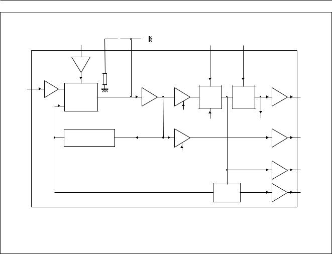
Fig.1 Block diagram.
DIAGRAM BLOCK |
(ADC) Converter |
speed high Triple |
|
|
Digital-to-Analog |
TDA8752
Semiconductors Philips
specification Product

Philips Semiconductors |
Product specification |
|
|
Triple high speed Analog-to-Digital |
|
|
TDA8752 |
|||
Converter (ADC) |
|
|
|
|
||
|
|
|
|
|
||
|
CLP |
|
RAGC |
CLKADC |
|
|
RCLP |
|
CLAMP |
|
|
|
|
|
|
|
|
|
|
|
|
VP |
CONTROL |
|
|
|
|
|
|
|
|
DAC |
|
|
|
|
|
|
|
|
|
|
150 |
|
|
|
|
|
RIN |
kW |
|
|
|
8 |
|
|
|
|
|
|
||
Vref |
MUX |
AGC |
|
ADC |
REGISTER |
ROR |
3 |
|
|
|
|
||
|
|
|
|
I2C-bus; 8 bits |
|
|
|
kW |
|
VCCAR |
|
|
|
|
|
|
|
(Or) |
8 |
|
|
45 |
|
|
|
OUTPUTS |
R0 to R7 |
|
kW |
|
|
|
|
|
|
|
|
|
|
8 |
|
|
DAC |
|
|
D |
|
OE |
|
|
|
|
D ³ R |
|
|
|
|
|
|
R |
|
|
|
|
|
|
1 |
8 |
|
|
5 |
|
|
|
RBOT |
|
|
|
|
|
7 |
||
|
|
|
|
|
|
|
|
REGISTER |
|
|
1 |
REGISTER |
|
|
FINE GAIN ADJUST |
|
|
|
|
|
|
|
|
COARSE GAIN ADJUST |
|
||
|
I2C-bus; 5 bits |
|
|
|
SERIAL |
|
|
|
|
I2C-bus; 7 bits |
|
||
|
(Fr) |
|
|
|
(Cr) |
|
|
|
|
|
|
I2C-BUS |
|
|
|
|
|
|
MGG364 |
|
|
HSYNCI |
RGAINC |
|
|
|
|
|
|
Fig.2 |
Red channel diagram. |
|
||
1999 Mar 09 |
|
|
|
5 |
|
|
Philips Semiconductors |
Product specification |
|
|
Triple high speed Analog-to-Digital
TDA8752
Converter (ADC)
handbook, full pagewidth |
Cz |
Cp |
|
|||||
COAST |
|
|
|
|
|
|
CKEXT |
INV |
|
|
|
|
|
|
|||
|
|
|
|
|
|
|||
CZ CP
|
I2C-bus; 1 bit |
|
|
|
|
|
|
||
|
|
(V level) |
|
|
|
|
|
|
|
|
|
|
|
loop filter |
|
12 to |
|
|
|
CKREF |
|
|
|
I2C-bus; |
|
100 MHz |
|
|
|
|
|
PHASE |
3 bits (Z) |
|
|
|
|
|
|
|
|
|
|
|
|
0°/180° |
|
||
|
edge selector |
FREQUENCY |
|
VCO |
|
MUX |
CKADCO |
||
|
DETECTOR |
|
|
|
|
|
|
||
|
I2C-bus; |
|
|
|
|
|
|
|
|
|
|
|
|
I2C-bus; |
|
|
|
|
|
|
1 bit |
|
I2C-bus; 5 bits |
|
phase selector A |
|
|
|
|
|
(edge) |
|
|
2 bits (VCO) |
I2C-bus; |
|
|
|
|
|
|
(Ip, Up, Do) |
|
I2C-bus; |
|
CLK |
|||
|
|
|
|
|
5 bits (Pa) |
|
|||
|
|
|
|
|
|
1 bit (Cka) |
|
ADC |
|
|
|
|
DIV N (100 to 4095) |
|
|
|
|
|
CKBO |
|
|
|
I2C-bus; 12 bits (Di) |
|
|
phase selector B |
|
|
I2C-bus; |
|
|
|
|
|
|
|
|
1 bit (Ckb) |
|
|
|
|
|
|
|
I2C-bus; 5 bits (Pb) |
|
|
|
|
|
|
|
|
|
|
|
|
|
|
|
|
|
|
|
|
|
|
CKAO |
|
|
|
|
|
|
|
SYNCHRO |
CKREFO |
|
|
|
|
|
|
|
|
|
|
MGG370 |
Fig.3 PLL diagram.
1999 Mar 09 |
6 |

Philips Semiconductors |
Product specification |
|
|
Triple high speed Analog-to-Digital
TDA8752
Converter (ADC)
PINNING
SYMBOL |
PIN |
DESCRIPTION |
|
|
|
n.c. |
1 |
not connected |
|
|
|
DEC2 |
2 |
main regulator decoupling input |
|
|
|
Vref |
3 |
gain stabilizer voltage reference input |
DEC1 |
4 |
main regulator decoupling input |
|
|
|
n.c. |
5 |
not connected |
|
|
|
RAGC |
6 |
red channel AGC output |
|
|
|
RBOT |
7 |
red channel ladder decoupling input (BOT) |
|
|
|
RGAINC |
8 |
red channel gain capacitor input |
|
|
|
RCLP |
9 |
red channel gain clamp capacitor input |
|
|
|
RDEC |
10 |
red channel gain regulator decoupling input |
|
|
|
VCCAR |
11 |
red channel gain analog power supply |
RIN |
12 |
red channel gain analog input |
|
|
|
AGNDR |
13 |
red channel gain analog ground |
|
|
|
GAGC |
14 |
green channel AGC output |
|
|
|
GBOT |
15 |
green channel ladder decoupling input (BOT) |
|
|
|
GGAINC |
16 |
green channel gain capacitor input |
|
|
|
GCLP |
17 |
green channel gain clamp capacitor input |
|
|
|
GDEC |
18 |
green channel gain regulator decoupling input |
|
|
|
VCCAG |
19 |
green channel gain analog power supply |
GIN |
20 |
green channel gain analog input |
|
|
|
AGNDG |
21 |
green channel gain analog ground |
|
|
|
BAGC |
22 |
blue channel AGC output |
|
|
|
BBOT |
23 |
blue channel ladder decoupling input (BOT) |
|
|
|
BGAINC |
24 |
blue channel gain capacitor input |
|
|
|
BCLP |
25 |
blue channel gain clamp capacitor input |
|
|
|
BDEC |
26 |
blue channel gain regulator decoupling input |
|
|
|
VCCAB |
27 |
blue channel gain analog power supply |
BIN |
28 |
blue channel gain analog input |
|
|
|
AGNDB |
29 |
blue channel gain analog ground |
|
|
|
n.c. |
30 |
not connected |
|
|
|
n.c. |
31 |
not connected |
|
|
|
I2C/3W |
32 |
selection input between I2C-bus (active HIGH) and 3-wire serial bus (active LOW) |
ADD1 |
33 |
I2C-bus address control input 1 |
ADD2 |
34 |
I2C-bus address control input 2 |
TCK |
35 |
scan test mode (active HIGH) |
|
|
|
1999 Mar 09 |
7 |

Philips Semiconductors |
Product specification |
|
|
Triple high speed Analog-to-Digital
TDA8752
Converter (ADC)
SYMBOL |
PIN |
DESCRIPTION |
|
|
|
TDO |
36 |
scan test output |
|
|
|
DIS |
37 |
I2C and 3W disable control input (disable at HIGH level) |
SEN |
38 |
select enable for 3-wire serial bus input (see Fig.10) |
|
|
|
SDA |
39 |
I2C/3W serial data input |
V |
40 |
logic I2C/3W digital power supply |
DDD |
|
|
V |
41 |
logic I2C/3W digital ground |
SSD |
|
|
SCL |
42 |
I2C/3W serial clock input |
n.c. |
43 |
not connected |
|
|
|
n.c. |
44 |
not connected |
|
|
|
ROR |
45 |
red channel ADC output bit out of range |
|
|
|
GOR |
46 |
green channel ADC output bit out of range |
|
|
|
BOR |
47 |
blue channel ADC output bit out of range |
|
|
|
OGNDB |
48 |
blue channel ADC output ground |
|
|
|
B0 |
49 |
blue channel ADC output bit 0 (LSB) |
|
|
|
n.c. |
50 |
not connected |
|
|
|
n.c. |
51 |
not connected |
|
|
|
B1 |
52 |
blue channel ADC output bit 1 |
|
|
|
B2 |
53 |
blue channel ADC output bit 2 |
|
|
|
B3 |
54 |
blue channel ADC output bit 3 |
|
|
|
B4 |
55 |
blue channel ADC output bit 4 |
|
|
|
B5 |
56 |
blue channel ADC output bit 5 |
|
|
|
B6 |
57 |
blue channel ADC output bit 6 |
|
|
|
B7 |
58 |
blue channel ADC output bit 7 (MSB) |
|
|
|
VCCOB |
59 |
blue channel ADC output power supply |
OGNDG |
60 |
green channel ADC output ground |
|
|
|
G0 |
61 |
green channel ADC output bit 0 (LSB) |
|
|
|
G1 |
62 |
green channel ADC output bit 1 |
|
|
|
G2 |
63 |
green channel ADC output bit 2 |
|
|
|
G3 |
64 |
green channel ADC output bit 3 |
|
|
|
G4 |
65 |
green channel ADC output bit 4 |
|
|
|
G5 |
66 |
green channel ADC output bit 5 |
|
|
|
G6 |
67 |
green channel ADC output bit 6 |
|
|
|
G7 |
68 |
green channel ADC output bit 7 (MSB) |
|
|
|
VCCOG |
69 |
green channel ADC output power supply |
OGNDR |
70 |
red channel ADC output ground |
|
|
|
R0 |
71 |
red channel ADC output bit 0 (LSB) |
|
|
|
1999 Mar 09 |
8 |

Philips Semiconductors |
Product specification |
|
|
Triple high speed Analog-to-Digital
TDA8752
Converter (ADC)
|
SYMBOL |
PIN |
|
|
DESCRIPTION |
|
|
|
|
|
|||
|
R1 |
72 |
red channel ADC output bit 1 |
|||
|
|
|
|
|||
|
R2 |
73 |
red channel ADC output bit 2 |
|||
|
|
|
|
|||
|
R3 |
74 |
red channel ADC output bit 3 |
|||
|
|
|
|
|||
|
R4 |
75 |
red channel ADC output bit 4 |
|||
|
|
|
|
|||
|
R5 |
76 |
red channel ADC output bit 5 |
|||
|
|
|
|
|||
|
R6 |
77 |
red channel ADC output bit 6 |
|||
|
|
|
|
|||
|
R7 |
78 |
red channel ADC output bit 7 (MSB) |
|||
|
|
|
|
|||
|
VCCOR |
79 |
red channel ADC output power supply |
|||
|
CKREFO |
80 |
reference output clock resynchronized horizontal pulse |
|||
|
|
|
|
|||
|
CKAO |
81 |
PLL clock output 3 (in phase with reference output clock) |
|||
|
|
|
|
|||
|
OGNDPLL |
82 |
PLL digital ground |
|||
|
|
|
|
|||
|
CKBO |
83 |
PLL clock output 2 |
|||
|
|
|
|
|||
|
CKADCO |
84 |
PLL clock output 1 (in phase with internal ADC clock) |
|||
|
|
|
|
|||
|
VCCO(PLL) |
85 |
PLL output power supply |
|||
|
DGND |
86 |
digital ground |
|||
|
|
|
|
|
|
|
|
|
|
87 |
output enable not (when |
|
is HIGH, the outputs are in high-impedance) |
|
OE |
|
OE |
|||
|
|
|
|
|||
|
PWDWN |
88 |
power-down control input (IC is in power-down mode when this pin is HIGH) |
|||
|
|
|
|
|||
|
CLP |
89 |
clamp pulse input (clamp active HIGH) |
|||
|
|
|
|
|||
|
HSYNC |
90 |
horizontal synchronization input pulse |
|||
|
|
|
|
|||
|
INV |
91 |
PLL clock output inverter command input (invert when HIGH) |
|||
|
|
|
|
|||
|
CKEXT |
92 |
external clock input |
|||
|
|
|
|
|||
|
COAST |
93 |
PLL coast command input |
|||
|
|
|
|
|||
|
CKREF |
94 |
PLL reference clock input |
|||
|
|
|
|
|||
|
VCCD |
95 |
digital power supply |
|||
|
AGNDPLL |
96 |
PLL analog ground |
|||
|
|
|
|
|||
|
CP |
97 |
PLL filter input |
|||
|
|
|
|
|||
|
CZ |
98 |
PLL filter input |
|||
|
|
|
|
|||
|
VCCAPLL |
99 |
PLL analog power supply |
|||
|
n.c. |
100 |
not connected |
|||
|
|
|
|
|
|
|
1999 Mar 09 |
9 |

Philips Semiconductors |
Product specification |
|
|
Triple high speed Analog-to-Digital
TDA8752
Converter (ADC)
|
|
|
n.c. |
|
CCA(PLL) |
|
CZ |
|
CP |
|
AGNDPLL |
|
CCD |
|
CKREF |
|
COAST |
|
CKEXT |
|
INV |
|
HSYNC |
|
CLP |
|
PWDWN |
|
OE |
|
DGND |
|
CCO(PLL) |
|
CKADCO |
|
CKBO |
|
OGNDPLL |
|
CKAO |
|
||
|
|
|
|
|
|
|
|
|
|
|
|
|
|
|
|
|
|
|
|
|
|
|
||||||||||||||||||||||
|
|
|
|
V |
|
|
|
|
V |
|
|
|
|
|
|
|
|
|
|
V |
|
|
|
|
|
|||||||||||||||||||
|
|
|
|
|
|
|
|
|
|
|
|
|
|
|
|
|
|
|
|
|
|
|
|
|
|
|
|
|
|
|
|
|
|
|
|
|
|
|
|
|
|
|
|
|
|
|
|
100 |
|
99 |
|
98 |
|
97 |
|
96 |
|
95 |
|
94 |
|
93 |
|
92 |
|
91 |
|
90 |
|
89 |
|
88 |
|
87 |
|
86 |
|
85 |
|
84 |
|
83 |
|
82 |
|
81 |
|
|
|
|
|
|
|
|
|
|
|
|
|
|
|
|
|
|
|
|
|
|
|
|
|
|
|
|
|
|
|
|
|
|
|
|
|
|
|
|
|
|
|
|
|
|
|
|
n.c. |
1 |
|
|
|
|
|
|
|
|
|
|
|
|
|
|
|
|
|
|
|
|
|
|
|
|
|
|
|
|
|
|
|
|
|
|
|
|
|
|
|
|
|
80 |
CKREFO |
|
|
|
|
|
|
|
|
|
|
|
|
|
|
|
|
|
|
|
|
|
|
|
|
|
|
|
|
|
|
|
|
|
|
|
|
|
|
|
|
|
VCCOR |
|||
DEC2 |
2 |
|
|
|
|
|
|
|
|
|
|
|
|
|
|
|
|
|
|
|
|
|
|
|
|
|
|
|
|
|
|
|
|
|
|
|
|
|
|
|
79 |
|||
Vref |
|
|
|
|
|
|
|
|
|
|
|
|
|
|
|
|
|
|
|
|
|
|
|
|
|
|
|
|
|
|
|
|
|
|
|
|
|
|
|
|
|
|||
3 |
|
|
|
|
|
|
|
|
|
|
|
|
|
|
|
|
|
|
|
|
|
|
|
|
|
|
|
|
|
|
|
|
|
|
|
|
|
|
|
78 |
R7 |
|||
DEC1 |
|
|
|
|
|
|
|
|
|
|
|
|
|
|
|
|
|
|
|
|
|
|
|
|
|
|
|
|
|
|
|
|
|
|
|
|
|
|
|
|
|
|||
4 |
|
|
|
|
|
|
|
|
|
|
|
|
|
|
|
|
|
|
|
|
|
|
|
|
|
|
|
|
|
|
|
|
|
|
|
|
|
|
|
77 |
R6 |
|||
n.c. |
|
|
|
|
|
|
|
|
|
|
|
|
|
|
|
|
|
|
|
|
|
|
|
|
|
|
|
|
|
|
|
|
|
|
|
|
|
|
|
|
|
|||
5 |
|
|
|
|
|
|
|
|
|
|
|
|
|
|
|
|
|
|
|
|
|
|
|
|
|
|
|
|
|
|
|
|
|
|
|
|
|
|
|
76 |
R5 |
|||
RAGC |
|
|
|
|
|
|
|
|
|
|
|
|
|
|
|
|
|
|
|
|
|
|
|
|
|
|
|
|
|
|
|
|
|
|
|
|
|
|
|
|
|
|||
6 |
|
|
|
|
|
|
|
|
|
|
|
|
|
|
|
|
|
|
|
|
|
|
|
|
|
|
|
|
|
|
|
|
|
|
|
|
|
|
|
75 |
R4 |
|||
RBOT |
|
|
|
|
|
|
|
|
|
|
|
|
|
|
|
|
|
|
|
|
|
|
|
|
|
|
|
|
|
|
|
|
|
|
|
|
|
|
|
|
|
|||
7 |
|
|
|
|
|
|
|
|
|
|
|
|
|
|
|
|
|
|
|
|
|
|
|
|
|
|
|
|
|
|
|
|
|
|
|
|
|
|
|
74 |
R3 |
|||
RGAINC |
|
|
|
|
|
|
|
|
|
|
|
|
|
|
|
|
|
|
|
|
|
|
|
|
|
|
|
|
|
|
|
|
|
|
|
|
|
|
|
|
R2 |
|||
8 |
|
|
|
|
|
|
|
|
|
|
|
|
|
|
|
|
|
|
|
|
|
|
|
|
|
|
|
|
|
|
|
|
|
|
|
|
|
|
|
73 |
||||
RCLP |
|
|
|
|
|
|
|
|
|
|
|
|
|
|
|
|
|
|
|
|
|
|
|
|
|
|
|
|
|
|
|
|
|
|
|
|
|
|
|
|
R1 |
|||
9 |
|
|
|
|
|
|
|
|
|
|
|
|
|
|
|
|
|
|
|
|
|
|
|
|
|
|
|
|
|
|
|
|
|
|
|
|
|
|
|
72 |
||||
RDEC |
|
|
|
|
|
|
|
|
|
|
|
|
|
|
|
|
|
|
|
|
|
|
|
|
|
|
|
|
|
|
|
|
|
|
|
|
|
|
|
|
R0 |
|||
10 |
|
|
|
|
|
|
|
|
|
|
|
|
|
|
|
|
|
|
|
|
|
|
|
|
|
|
|
|
|
|
|
|
|
|
|
|
|
|
|
71 |
||||
VCCAR |
|
|
|
|
|
|
|
|
|
|
|
|
|
|
|
|
|
|
|
|
|
|
|
|
|
|
|
|
|
|
|
|
|
|
|
|
|
|
|
|
OGNDR |
|||
11 |
|
|
|
|
|
|
|
|
|
|
|
|
|
|
|
|
|
|
|
|
|
|
|
|
|
|
|
|
|
|
|
|
|
|
|
|
|
|
|
70 |
||||
RIN |
|
|
|
|
|
|
|
|
|
|
|
|
|
|
|
|
|
|
|
|
|
|
|
|
|
|
|
|
|
|
|
|
|
|
|
|
|
|
|
|
VCCOG |
|||
12 |
|
|
|
|
|
|
|
|
|
|
|
|
|
|
|
|
|
|
|
|
|
|
|
|
|
|
|
|
|
|
|
|
|
|
|
|
|
|
|
69 |
||||
AGNDR |
|
|
|
|
|
|
|
|
|
|
|
|
|
|
|
|
|
|
|
|
|
|
|
|
|
|
|
|
|
|
|
|
|
|
|
|
|
|
|
|
G7 |
|||
13 |
|
|
|
|
|
|
|
|
|
|
|
|
|
|
|
|
|
|
|
|
|
|
|
|
|
|
|
|
|
|
|
|
|
|
|
|
|
|
|
68 |
||||
GAGC |
|
|
|
|
|
|
|
|
|
|
|
|
|
|
|
|
|
|
|
|
|
|
|
|
|
|
|
|
|
|
|
|
|
|
|
|
|
|
|
|
G6 |
|||
14 |
|
|
|
|
|
|
|
|
|
|
|
|
|
|
|
|
|
|
|
|
|
|
|
|
|
|
|
|
|
|
|
|
|
|
|
|
|
|
|
67 |
||||
GBOT |
|
|
|
|
|
|
|
|
|
|
|
|
|
|
|
|
|
|
|
|
|
|
|
|
|
|
|
|
|
|
|
|
|
|
|
|
|
|
|
|
G5 |
|||
15 |
|
|
|
|
|
|
|
|
|
|
|
|
|
|
|
|
|
TDA8752 |
|
|
|
|
|
|
|
|
|
|
|
|
|
|
|
66 |
||||||||||
|
|
|
|
|
|
|
|
|
|
|
|
|
|
|
|
|
|
|
|
|
|
|
|
|
|
|
|
|
|
|
|
|
|
|
|
|
|
|||||||
GGAINC |
16 |
|
|
|
|
|
|
|
|
|
|
|
|
|
|
|
|
|
|
|
|
|
|
|
|
|
|
|
|
|
|
|
|
|
|
|
|
|
|
|
65 |
G4 |
||
GCLP |
|
|
|
|
|
|
|
|
|
|
|
|
|
|
|
|
|
|
|
|
|
|
|
|
|
|
|
|
|
|
|
|
|
|
|
|
|
|
|
|
G3 |
|||
17 |
|
|
|
|
|
|
|
|
|
|
|
|
|
|
|
|
|
|
|
|
|
|
|
|
|
|
|
|
|
|
|
|
|
|
|
|
|
|
|
64 |
||||
GDEC |
|
|
|
|
|
|
|
|
|
|
|
|
|
|
|
|
|
|
|
|
|
|
|
|
|
|
|
|
|
|
|
|
|
|
|
|
|
|
|
|
G2 |
|||
18 |
|
|
|
|
|
|
|
|
|
|
|
|
|
|
|
|
|
|
|
|
|
|
|
|
|
|
|
|
|
|
|
|
|
|
|
|
|
|
|
63 |
||||
VCCAG |
|
|
|
|
|
|
|
|
|
|
|
|
|
|
|
|
|
|
|
|
|
|
|
|
|
|
|
|
|
|
|
|
|
|
|
|
|
|
|
|
G1 |
|||
19 |
|
|
|
|
|
|
|
|
|
|
|
|
|
|
|
|
|
|
|
|
|
|
|
|
|
|
|
|
|
|
|
|
|
|
|
|
|
|
|
62 |
||||
GIN |
|
|
|
|
|
|
|
|
|
|
|
|
|
|
|
|
|
|
|
|
|
|
|
|
|
|
|
|
|
|
|
|
|
|
|
|
|
|
|
|
G0 |
|||
20 |
|
|
|
|
|
|
|
|
|
|
|
|
|
|
|
|
|
|
|
|
|
|
|
|
|
|
|
|
|
|
|
|
|
|
|
|
|
|
|
61 |
||||
AGNDG |
|
|
|
|
|
|
|
|
|
|
|
|
|
|
|
|
|
|
|
|
|
|
|
|
|
|
|
|
|
|
|
|
|
|
|
|
|
|
|
|
OGNDG |
|||
21 |
|
|
|
|
|
|
|
|
|
|
|
|
|
|
|
|
|
|
|
|
|
|
|
|
|
|
|
|
|
|
|
|
|
|
|
|
|
|
|
60 |
||||
BAGC |
|
|
|
|
|
|
|
|
|
|
|
|
|
|
|
|
|
|
|
|
|
|
|
|
|
|
|
|
|
|
|
|
|
|
|
|
|
|
|
|
VCCOB |
|||
22 |
|
|
|
|
|
|
|
|
|
|
|
|
|
|
|
|
|
|
|
|
|
|
|
|
|
|
|
|
|
|
|
|
|
|
|
|
|
|
|
59 |
||||
BBOT |
|
|
|
|
|
|
|
|
|
|
|
|
|
|
|
|
|
|
|
|
|
|
|
|
|
|
|
|
|
|
|
|
|
|
|
|
|
|
|
|
B7 |
|||
23 |
|
|
|
|
|
|
|
|
|
|
|
|
|
|
|
|
|
|
|
|
|
|
|
|
|
|
|
|
|
|
|
|
|
|
|
|
|
|
|
58 |
||||
BGAINC |
|
|
|
|
|
|
|
|
|
|
|
|
|
|
|
|
|
|
|
|
|
|
|
|
|
|
|
|
|
|
|
|
|
|
|
|
|
|
|
|
B6 |
|||
24 |
|
|
|
|
|
|
|
|
|
|
|
|
|
|
|
|
|
|
|
|
|
|
|
|
|
|
|
|
|
|
|
|
|
|
|
|
|
|
|
57 |
||||
BCLP |
|
|
|
|
|
|
|
|
|
|
|
|
|
|
|
|
|
|
|
|
|
|
|
|
|
|
|
|
|
|
|
|
|
|
|
|
|
|
|
|
B5 |
|||
25 |
|
|
|
|
|
|
|
|
|
|
|
|
|
|
|
|
|
|
|
|
|
|
|
|
|
|
|
|
|
|
|
|
|
|
|
|
|
|
|
56 |
||||
BDEC |
|
|
|
|
|
|
|
|
|
|
|
|
|
|
|
|
|
|
|
|
|
|
|
|
|
|
|
|
|
|
|
|
|
|
|
|
|
|
|
|
B4 |
|||
26 |
|
|
|
|
|
|
|
|
|
|
|
|
|
|
|
|
|
|
|
|
|
|
|
|
|
|
|
|
|
|
|
|
|
|
|
|
|
|
|
55 |
||||
VCCAB |
|
|
|
|
|
|
|
|
|
|
|
|
|
|
|
|
|
|
|
|
|
|
|
|
|
|
|
|
|
|
|
|
|
|
|
|
|
|
|
|
B3 |
|||
27 |
|
|
|
|
|
|
|
|
|
|
|
|
|
|
|
|
|
|
|
|
|
|
|
|
|
|
|
|
|
|
|
|
|
|
|
|
|
|
|
54 |
||||
BIN |
|
|
|
|
|
|
|
|
|
|
|
|
|
|
|
|
|
|
|
|
|
|
|
|
|
|
|
|
|
|
|
|
|
|
|
|
|
|
|
|
B2 |
|||
28 |
|
|
|
|
|
|
|
|
|
|
|
|
|
|
|
|
|
|
|
|
|
|
|
|
|
|
|
|
|
|
|
|
|
|
|
|
|
|
|
53 |
||||
AGNDB |
|
|
|
|
|
|
|
|
|
|
|
|
|
|
|
|
|
|
|
|
|
|
|
|
|
|
|
|
|
|
|
|
|
|
|
|
|
|
|
|
B1 |
|||
29 |
|
|
|
|
|
|
|
|
|
|
|
|
|
|
|
|
|
|
|
|
|
|
|
|
|
|
|
|
|
|
|
|
|
|
|
|
|
|
|
52 |
||||
n.c. |
|
|
|
|
|
|
|
|
|
|
|
|
|
|
|
|
|
|
|
|
|
|
|
|
|
|
|
|
|
|
|
|
|
|
|
|
|
|
|
|
n.c. |
|||
30 |
|
|
|
|
|
|
|
|
|
|
|
|
|
|
|
|
|
|
|
|
|
|
|
|
|
|
|
|
|
|
|
|
|
|
|
|
|
|
|
51 |
||||
31 |
|
32 |
|
33 |
|
34 |
|
35 |
|
36 |
|
37 |
|
38 |
|
39 |
|
40 |
|
41 |
|
42 |
|
43 |
|
44 |
|
45 |
|
46 |
|
47 |
|
48 |
|
49 |
|
50 |
|
|
|
|
|
|
|
|
|
|
|
|
|
|
|
|
|
|
|
|
|
|
|
|
|
|
|
|
|
|
|
|
|
|
|
|
|
|
|
n.c. |
|
C/3W |
|
ADD1 |
|
ADD2 |
|
TCK |
|
TDO |
|
DIS |
|
SEN |
|
SDA |
|
DDD |
|
SSD |
|
SCL |
|
n.c. |
|
n.c. |
|
ROR |
|
GOR |
|
BOR |
|
OGNDB |
|
B0 |
|
n.c. |
|
I |
|
|
|
|
|
|
|
|
V |
|
V |
|
|
|
|
|
|
|
|
|
|||||||||||||||||
|
2 |
|
|
|
|
|
|
|
|
|
|
|
|
|
|
|
|
|
|
|
|
|
|
|
|
|
|
|
|
|
|
|
|
|
|
|
|
|
MGG362
Fig.4 Pin configuration.
1999 Mar 09 |
10 |
Philips Semiconductors |
Product specification |
|
|
Triple high speed Analog-to-Digital
TDA8752
Converter (ADC)
FUNCTIONAL DESCRIPTION
This triple high-speed 8-bit ADC is designed to convert RGB signals, from a PC or work station, into data used by a LCD driver (pixel clock up to 200 MHz, using 2 ICs).
IC analog video inputs
The video inputs are internally DC polarized. These inputs are AC coupled externally.
Clamps
Three independent parallel clamping circuits are used to clamp the video input signals on the black level and to control the brightness level. The clamping code is programmable between code -63.5 and +64 in steps of 1¤2LSB. The programming of the clamp value is achieved via an 8-bit DAC. Each clamp must be able to correct an offset from ±0.1 V to ±10 mV within 300 ns, and correct the total offset in 10 lines.
The clamps are controlled by an external TTL positive going pulse (pin CLP). The drop of the video signal is <1 LSB.
Normally, the circuit operates with a 0 code clamp, corresponding to the 0 ADC code. This clamp code can be changed from -63.5 to +64 as represented in Fig.7,
in steps of 1¤2LSB. The digitized video signal is always between code 0 and code 255 of the ADC.
Variable gain amplifier
Three independent variable gain amplifiers are used to provide, to each channel, a full-scale input range signal to the 8-bit ADC. The gain adjustment range is designed so that, for an input range varying from 0.4 to 1.2 V (p-p), the output signal corresponds to the ADC full-scale input of 1 V (p-p).
To ensure that the gain does not vary over the whole operating temperature range, an external reference of +2.5 V DC, (Vref with a 100 ppm/°C maximum variation) supplied externally, is used to calibrate the gain at the beginning of each video line before the clamp pulse using the following principle.
A differential of 0.156 V (p-p) (1¤16Vref) reference signal is generated internally from the reference voltage (Vref). During the synchronization part of the video line, the multiplexer, controlled by the TTL synchronization signal (HSYNCI, coming from HSYNC; see Fig.1) with a width equal to one of the video synchronization signals
(e.g. signal coming from a synchronization separator), is switched between the two amplifiers.
The output of the multiplexer is either the normal video signal or the 0.156 V reference signal (during HSYNC).
The corresponding ADC outputs are then compared to a pre-set value loaded in a register. Depending on the result of the comparison, the gain of the variable gain amplifiers is adjusted (coarse gain control; see Figs 2 and 8).
The three 7-bit registers receive data via a serial interface to enable the gain to be programmed.
The pre-set value loaded in the 7-bit register is chosen between approximately 67 codes to ensure the full-scale input range (see Fig.8). A contrast control can be achieved using these registers. In this case care should be taken to stay within the allowed code range (32 to 99).
A fine correction using three 5-bit DACs, also controlled via the serial interface, is used to finely tune the gain of the three channels (fine gain control; see Figs 2 and 9) and to compensate the channel-to-channel gain mismatch.
With a full scale ADC input, the resolution of the fine register corresponds to 1¤2LSB peak-to-peak variation.
To use these gain controls correctly, it is recommended to fix the coarse gain (to have a full-scale ADC input signal) to within 4LSB and then adjust it with the fine gain.
The gain is adjusted during HSYNC. During this time the output signal is not related to the amplified input signal. The outputs, when the coarse gain system is stable, is related to the programmed coarse code (see Fig.8).
ADCs
The ADCs are 8-bit with a maximum clock frequency of 100 Msps. The ADCs input range is 1 V (p-p) full-scale. One out of range bit exists per channel (ROR, GOR and BOR). It will be at logic 1 when the signal is out of range of the full scale of the ADCs.
Pipeline delay in the ADCs is 1 clock cycle from sampling to data output.
The ADCs reference ladders regulators are integrated.
ADC outputs
ADC outputs are straight binary. An output enable pin (OE; active LOW) enables the output status between active and high-impedance (OE = HIGH) to be switched; it is recommended to load the outputs with a 10 pF capacitive load. The timing must be checked very carefully if the capacitive load is more than 10 pF.
1999 Mar 09 |
11 |
 Loading...