


MPC2106A
Motorola MPC2106A, MPC2106ASG66, MPC2106B, MPC2105ASG66, MPC2105B Datasheet
...
MPC2105A•MPC2106A•MPC2105B•MPC2106B
1
MOTOROLA FAST SRAM
512KB and 1MB BurstRAM
Secondary Cache Modules for
PowerPC PReP/CHRP Platforms
The MPC2105A/B and the MPC2106A/B are designed to provide burstable, high
performance L2 cache for the PowerPC 60x microprocessor family in conformance
with the PowerPC Reference Platform (PReP) and the PowerPC Common Hardware
Reference Platform (CHRP) specifications.
The MPC2105A/B and MPC2106A/B utilize synchronous BurstRAMs. The
modules are configured as 64K x 72, and 128K x 72 bits in a 178 (89 x 2) pin DIMM
format. The MPC2105A/B uses four of the 3 V 64K x 18; the MPC2106A/B uses eight
of the 3 V 64K x 18. For tag bits, a 5 V cache ta g R AM configured as 16K x 12 for tag
field plus 16K x 2 for valid and dirty status bits is used.
Bursts can be initiated with the ADS
signal. Subsequent burst addresses are
generated internal to the BurstRAM by the CNTEN signal.
Write cycles are internally self timed and are initiated by the rising edge of the clock
(CLKx) inputs. Eight write enables are provided for byte write control.
Presence detect pins are available for auto configuration of the cache control.
The module family pinout will support 5 V and 3.3 V components for a clear path
to lower voltage and power savings. Both power supplies must be connected.
All of these cache modules are plug and pin compatible with each other.
• PowerPC–style Burst Counter on Chip
• Flow–Through Data I/O
• Plug and Pin Compatibility
• Multiple Clock Pins for Reduced Loading
• 20 Ω Series Resistors on DL and DH Pins for Noise
Reduction (MPC2105A/6A)
• All Cache Data and Tag I/Os are LVTTL (3.3 V) Compatible
• Three State Outputs
• Byte Write Capability
• Fast Module Clock Rates: Up to 66 MHz
• Fast SRAM Access Times: 10 ns for Tag RAM Match
9 ns for Data RAM
• Decoupling Capacitors for Each Fast Static RAM
• High Quality Multi–Layer FR4 PWB With Separate Power and Ground Planes
• 178 Pin Card Edge Module
• Burndy Connector, Part Number: ELF178KSC–3Z50
BurstRAM is a trademark of Motorola.
The PowerPC name is a trademark of IBM Corp., used under license therefrom.
Order this document
by MPC2105A/D
MOTOROLA
SEMICONDUCTOR TECHNICAL DATA
MPC2105A
MPC2106A
MPC2105B
MPC2106B
178–LEAD CARD EDGE
TOP VIEW
MPC2105A/B CASE 1132A–01
MPC2106A/B CASE 1132–01
80
25
24
1
48
47
REV 1
12/19/96
Motorola, Inc. 1996
MPC2105A•MPC2106A•MPC2105B•MPC2106B
2
MOTOROLA FAST SRAM
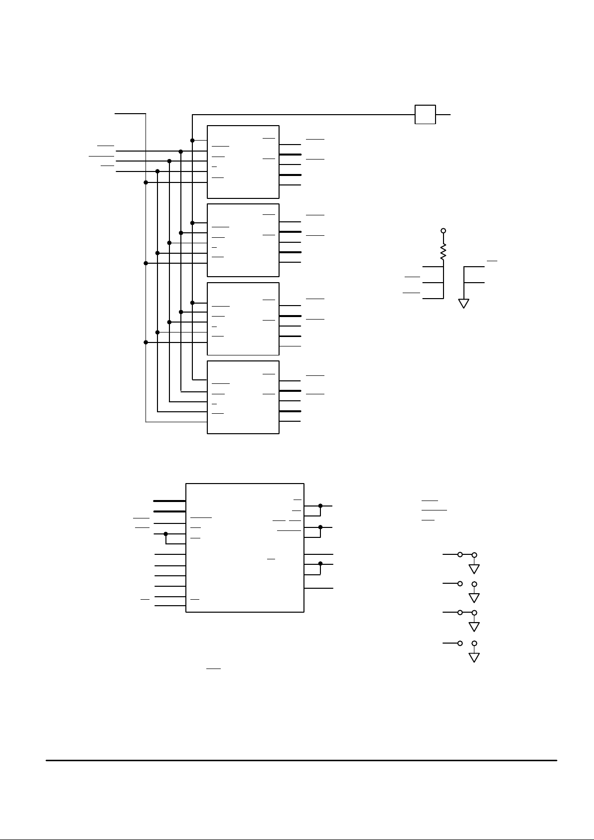
MPC2105A/B BLOCK DIAGRAM
A0 = NC
CLK3 = NC
CLK4 = NC
ALE = NC
ADS1
= NC
CNTEN1
= NC
CG1
= NC
ADDR0 = NC
ADDR1 = NC
DH24 – DH31 + DP3
CLK1
DL16 – DL23 + DP6
DL24 – DL31 + DP7
Note: BA28 is tied to SA0 on SRAM;
BA27 is tied to SA1 on SRAM;
STANDBY is tied to SE3
on SRAM.
69F618ATQ
G
SE1
ADSC
CG0
SA
ADV
ADS0
CWE1
CLK0
DH0 – DH7 + DP0
DH8 – DH15 + DP1
CWE0
CNTEN0
CWE2
CLK0
DH16 – DH23 + DP2
CWE3
K
DQB
DQA
CWE4
SBB
SBA
CLK1
DL0 – DL7 + DP4
DL8 – DL15 + DP5
CWE5
CWE6
CWE7
V
SS
K
DQB
DQA
SBB
SBA
K
DQB
DQA
SBB
SBA
K
DQB
DQA
SBB
SBA
69F618ATQ
69F618ATQ
69F618ATQ
G
SE1
ADSC
SA
ADV
G
SE1
ADSC
SA
ADV
G
SE1
ADSC
SA
ADV
’244
A13 – A28
BA13 – BA28
PD3
PD2
PD1
PD0
J2
J0
J3
A13 – A26
A1 – A12
TCLR
TWE
CLK2
MATCH
VALIDIN
DIRTYIN
TG
TAG: 16K x 12 + V + D
A0 – A13
RESET
TAG0 –11
TAH, TAG
, TAD
SFUNC, SG
SW
TW
K
VALIDD
DIRTYD
TG
TT1, WTD, E1
E2, PWRDN
V
SS
V
CC
via 100
Ω
WTQ
TA
, VALIDQ
V
CCQ
V
DD
NC
MATCH
DIRTYOUT
DIRTYQ
SE2
SGW
ADSP
SW
ZZ
SRAM TIE OFF
J1
V
CC
V
CC
V
DD
MPC2105A•MPC2106A•MPC2105B•MPC2106B
3
MOTOROLA FAST SRAM
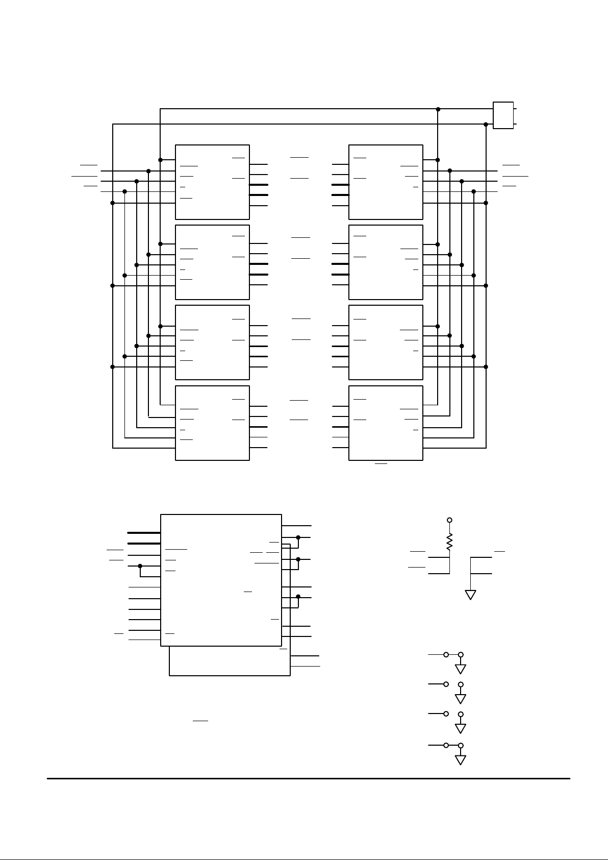
MPC2106A/B BLOCK DIAGRAM
A13 – A26
A0 – A11
TCLR
TWE
CLK2
MATCH
VALIDIN
DIRTYIN
TG
TAG: 16K x 12 + V + D
A0 – A13
RESET
TAG0 –11
TAH, TAG, TAD
SFUNC, SG
SW
TW
K
E2
VALIDD
DIRTYD
TG
ALE = NC
ADDR0 = NC
ADDR1 = NC
DH24 – DH31 + DP3
CLK4
DL16 – DL23 + DP6
DL24 – DL31 + DP7
TT1, WTD
PWRDN
V
SS
V
CC
via 100
Ω
WTQ
TA
, VALIDQ
V
CCQ
V
DD
NC
A12
69F618ATQ
G
SE1
ADSC
CG0
SA
ADV
ADS0
CWE0
CLK0
DH0 – DH7 + DP0
DH8 – DH15 + DP1
CWE1
CNTEN0
CWE2
CLK1
DH16 – DH23 + DP2
CWE3
K
DQB
DQA
CWE4
SBB
SBA
CLK3
DL0 – DL7 + DP4
DL8 – DL15 + DP5
CWE5
CWE6
CWE7
K
DQB
DQA
SBB
SBA
K
DQB
DQA
SBB
SBA
K
DQB
DQA
SBB
SBA
69F618ATQ
69F618ATQ
69F618ATQ
G
SE1
ADSC
SA
ADV
G
SE1
ADSC
SA
ADV
G
SE1
ADSC
SA
ADV
’244
A13 – A28
BA13 – BA28
PD3
PD2
PD1
PD0
J2
J0
J3
J1
69F618ATQ
G
SE2
ADSC
CG1
SA
ADV
ADS1
CNTEN1
K
DQA
DQB
SBA
SBB
K
DQA
DQB
SBA
SBB
K
DQA
DQB
SBA
SBB
K
DQA
DQB
SBA
SBB
69F618ATQ
69F618ATQ
69F618ATQ
G
SE2
ADSC
SA
ADV
G
SE2
ADSC
SA
ADV
G
SE2
ADSC
SA
ADV
A12
BA12
BANK A: SE2 TIED TO.
V
DD
VIA 100
Ω.
BANK B: SE1 TIED TO. V
SS
MATCH
DIRTYOUT
DIRTYQ
E1
V
CC
E2
A12
E1 V
SS
Note: BA28 is tied to SA0 on SRAM;
BA27 is tied to SA1 on SRAM;
STANDBY is tied to SE3
on SRAM.
SGW
ADSP
SW
ZZ
SRAM TIE OFF
V
DD
V
CC
V
CC
MPC2105A•MPC2106A•MPC2105B•MPC2106B
4
MOTOROLA FAST SRAM
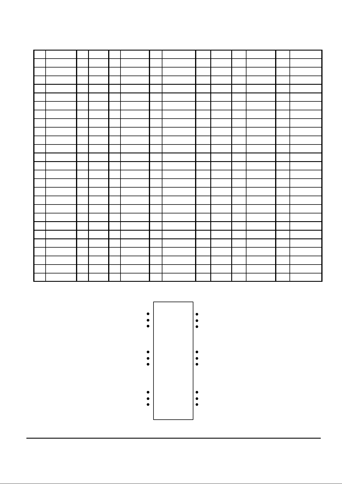
PIN ASSIGNMENT 178–LEAD DIMM
Pin Name Pin Name Pin Name Pin Name Pin Name Pin Name Pin Name
1 V
SS
27 DH0 53 DL1 79 V
SS
105 DH14 131 DL17 157 A22
2 PD0/IDSCLK 28 DP0 54 DL0 80 A7 106 DH13 132 CWE6 158 A20
3 PD2 29 V
SS
55 V
SS
81 A5 107 V
CC
133 DL15 159 V
SS
4 DH30 30 CLK1 56 CLK2 82 A3 108 DH10 134 DL13 160 A18
5 DH28 31 V
SS
57 V
SS
83 A0 109 DH8 135 V
SS
161 A16
6 DH26 32 DL28 58 DP4 84 V
CC
110 CWE1 136 DL10 162 A15
7 DH24 33 DL26 59 CG0 85 TCLR 111 DH6 137 DL8 163 A14
8 V
DD
34 DL24 60 CG1 86 MATCH 112 V
DD
138 CWE5 164 V
DD
9 DP3 35 DP7 61 V
DD
87 TG 113 DH4 139 DL6 165 A10
10 DH22 36 V
CC
62 ADDR0 88 DIRTYIN 114 V
SS
140 V
DD
166 A8
11 DH20 37 DL22 63 RESERVED 89 V
SS
115 CLK0 141 DL5 167 A6
12 DH19 38 DL20 64 ADS0 90 V
SS
116 V
SS
142 DL2 168 V
SS
13 V
SS
39 DL18 65 ADS1 91 PD1/IDSDATA 117 DH1 143 V
SS
169 A4
14 DH17 40 DL16 66 A28 92 PD3 118 CWE0 144 CLK3 170 A2
15 DP2 41 V
SS
67 A26 93 DH31 119 DL31 145 V
SS
171 A1
16 DH15 42 DP6 68 A25 94 DH29 120 DL30 146 CLK4 172 BURSTMODE
17 DH12 43 DL14 69 A23 95 DH27 121 V
SS
147 V
SS
173 V
CC
18 V
CC
44 DL12 70 V
SS
96 DH25 122 DL29 148 CWE4 174 VALIDIN
19 DH11 45 DL11 71 A21 97 V
DD
123 DL27 149 ALE 175 TWE
20 DH9 46 V
SS
72 A19 98 CWE3 124 DL25 150 V
DD
176 STANDBY
21 DP1 47 DL9 73 A17 99 DH23 125 V
CC
151 ADDR1 177 DIRTYOUT
22 DH7 48 DP5 74 A13 100 DH21 126 CWE7 152 RESERVED 178 V
SS
23 V
DD
49 DL7 75 V
DD
101 DH18 127 DL23 153 CNTEN0
24 DH5 50 DL4 76 A12 102 V
SS
128 DL21 154 CNTEN1
25 DH3 51 V
DD
77 A11 103 DH16 129 DL19 155 A27
26 DH2 52 DL3 78 A9 104 CWE2 130 V
SS
156 A24
NOTE:V
CC
and V
DD
must be connected on all modules.
TOP VIEW
1
24
25
89
90
113
114
178
47136
48137

MPC2105A•MPC2106A•MPC2105B•MPC2106B
5
MOTOROLA FAST SRAM
PIN DESCRIPTIONS
Pin Locations Symbol
Type Description
66, 67, 68, 69, 71, 72, 73, 74,
76, 77, 78, 80, 81, 82, 83,
155, 156, 157, 158, 160, 161,
162, 163, 165, 166, 167, 169,
170, 171
A0 – A28 Input Address Inputs – (MSB:0, LSB:28).
62 ADDR0 Input Least significant address bit when asynchronous Data RAMs are used.
151 ADDR1 Input Next to least significant address bit when asynchronous Data RAMs are used.
64, 65 ADS0, ADS1 Input Data RAM Address Strobe – For MPC2105A/B use ADS0 only. For
MPC2106A/B use ADS0
, ADS1.
149 ALE Input Data RAM Address Latch Enable – Use for asynchronous Data RAM only .
172 BURSTMODE Input Burstmode. 0 = Linear, 1 = Interleaved.
59, 60 CG0,
CG1
Input Data RAM Output Enables – For MPC2105A/B use CG0 only. For
MPC2106A/B use CG0
, CG1.
30, 56, 115, 144, 146 CLK0 – CLK4 Input Clock Inputs – CLK2 is for T ag RAM, CLK0, 1, 3, and 4 are for Data RAMs only .
For MPC2106A/B use all the clocks. For MPC2105A/B use CLK0 – CLK2 only.
153, 154 CNTEN0,
CNTEN1
Input Data RAM Count Enables – For MPC2105A/B use CNTEN0 only. For
MPC2106A/B use CNTEN0
, CNTEN1.
98, 104, 110, 118,
126, 132, 138, 148
CWE0 – CWE7 Input Data RAM Write Enables – (MSB:0, LSB:7).
4, 5, 6, 7, 10, 11, 12, 14, 16,
17, 19, 20, 22, 24, 25, 26, 27,
93, 94, 95, 96, 99, 100, 101,
103, 105, 106, 108, 109, 111,
113, 117
DH0 – DH31 I/O High Data Bus – (MSB:0, LSB:31).
88 DIRTYIN Input Dirty input bit.
177 DIRTYOUT Output Dirty output bit.
32, 33, 34, 37, 38, 39, 40, 43,
44, 45, 47, 49, 50, 52, 53, 54,
119, 120, 122, 123, 124, 127,
128, 129, 131, 133, 134, 136,
137, 139, 141, 142
DL0 – DL31 I/O Low Data Bus – (MSB:0, LSB:31).
9, 15, 21, 28, 35, 42, 48, 58 DP0 – DP7 I/O Data Parity Bits – (MSB:0, LSB:7)
86 MATCH Output Tag RAM active high match indication.
2 PD0/IDSCLK Input Presence detect bit 0/EEPROM serial clock. (EEPROM option only).
91 PD1/IDSDATA I/O Presence detect bit 1/EEPROM serial data. (EEPROM option only).
3, 92 PD2, PD3 Output Presence detect bits.
63, 152 RESERVED Reserved pin.
176 STANDBY Input Standby pin. Reduces standby power consumption.
85 TCLR Input Tag RAM clear.
87 TG Input Tag RAM output enable.
175 TWE Input Tag RAM write enable.
174 VALIDIN Input Tag RAM valid bit.
18, 36, 84, 107, 125, 173 V
CC
Input + 5 V power supply . Must be connected.
8, 23, 51, 61, 75, 97, 112,
140, 150, 164
V
DD
Input + 3.3 V power supply . Must be connected.
1, 13, 29, 31, 41, 46, 55, 57,
70, 79, 89, 90, 102, 114,
116, 121, 130, 135, 143,
145, 147, 159, 168, 178
V
SS
Input Ground.
MPC2105A•MPC2106A•MPC2105B•MPC2106B
6
MOTOROLA FAST SRAM
DATA RAM MCM69F618A SYNCHRONOUS TRUTH TABLE (See Notes 1, 2, and 3)
STANDBY
ADSx CNTENx CWEx CLKx Address Used Operation
H L X X L–H N/A Deselected
L L X L L–H External Address Write Cycle, Begin Burst
L L X H L–H External Address Read Cycle, Begin Burst
X H L L L–H Next Address Write Cycle, Continue Burst
X H L H L–H Next Address Read Cycle, Continue Burst
X H H L L–H Current Address Write Cycle, Suspend Burst
X H H H L–H Current Address Read Cycle, Suspend Burst
NOTES:
1. X means Don’t Care.
2. All inputs except CG
must meet set–up and hold times for the low–to–high transition of clock (CLK0 – CLK4).
3. Wait states are inserted by suspending burst.
ASYNCHRONOUS TRUTH TABLE (See Notes 1 and 2)
Operation
CG I/O Status
Read L Data Out (DQ0 – DQ8)
Read H High–Z
Write X High–Z — Data In
Deselected X High–Z
NOTES:
1. X means Don’t Care.
2. For a write operation following a read operation, CG
must be high before the input data
required set–up time and held high through the input data hold time.
ABSOLUTE MAXIMUM RATINGS (Voltages Referenced to V
SS
= 0 V)
Rating
Symbol Value Unit
Power Supply Voltage V
CC
– 0.5 to + 7.0 V
Voltage Relative to V
SS
V
in
, V
out
– 0.5 to V
CC
+ 0.5 V
Output Current (per I/O) Data RAM
Tag
I
out
± 30
± 20
mA
Power Dissipation MPC2105A/B
MPC2106A/B
P
D
4.6
9.2
W
Temperature Under Bias T
bias
– 10 to + 85 °C
Operating Temperature T
A
0 to +70 °C
Storage Temperature T
stg
– 55 to + 125 °C
NOTE: Permanent device damage may occur if ABSOLUTE MAXIMUM RATINGS are
exceeded. Functional operation should be restricted to RECOMMENDED OPER-
ATING CONDITIONS. Exposure to higher than recommended voltages for
extended periods of time could affect device reliability.
This device contains circuitry to protect the
inputs against damage due to high static volt-
ages or electric fields; however, it is advised
that normal precautions be taken to avoid
application of any voltage higher than maxi-
mum rated voltages to this high–impedance
circuit.
This BiCMOS memory circuit has been
designed to meet the dc and ac specifications
shown in the tables, after thermal equilibrium
has been established.
This device contains circuitry that will
ensure the output devices are in High–Z at
power up.
 Loading...