MOTOROLA MPSA14RLRM, MPSA13RLRP, MPSA13, MPSA14RLRP, MPSA14RLRA Datasheet
...
MOTOROLA
SEMICONDUCTOR TECHNICAL DATA
Order this document by MPSA13/D
Darlington Transistors
NPN Silicon
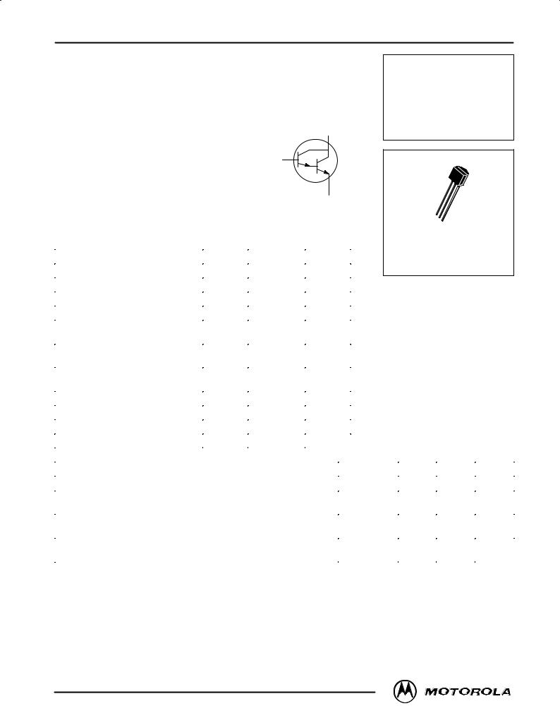
COLLECTOR 3
BASE 2
EMITTER 1
MAXIMUM RATINGS
Rating |
Symbol |
Value |
Unit |
|
|
|
|
Collector± Emitter Voltage |
VCES |
30 |
Vdc |
Collector± Base Voltage |
VCBO |
30 |
Vdc |
Emitter± Base Voltage |
VEBO |
10 |
Vdc |
Collector Current Ð Continuous |
IC |
500 |
mAdc |
Total Device Dissipation @ TA = 25°C |
PD |
625 |
mW |
Derate above 25°C |
|
5.0 |
mW/°C |
|
|
|
|
Total Device Dissipation @ TC = 25°C |
PD |
1.5 |
Watts |
Derate above 25°C |
|
12 |
mW/°C |
|
|
|
|
Operating and Storage Junction |
TJ, Tstg |
± 55 to +150 |
°C |
Temperature Range |
|
|
|
|
|
|
|
THERMAL CHARACTERISTICS
Characteristic |
Symbol |
Max |
Unit |
|
|
|
|
Thermal Resistance, Junction to Ambient |
RqJA |
200 |
°C/W |
Thermal Resistance, Junction to Case |
RqJC |
83.3 |
°C/W |
ELECTRICAL CHARACTERISTICS (TA = 25°C unless otherwise noted)
MPSA13 MPSA14*
*Motorola Preferred Device
1
2 3
CASE 29±04, STYLE 1 TO±92 (TO±226AA)
Characteristic |
Symbol |
Min |
Max |
Unit |
|
|
|
|
|
OFF CHARACTERISTICS |
|
|
|
|
|
|
|
|
|
Collector± Emitter Breakdown Voltage |
V(BR)CES |
30 |
Ð |
Vdc |
(IC = 100 μAdc, IB = 0) |
|
|
|
|
Collector Cutoff Current |
ICBO |
Ð |
100 |
nAdc |
(VCB= 30 Vdc, IE = 0) |
|
|
|
|
Emitter Cutoff Current |
IEBO |
Ð |
100 |
nAdc |
(VEB= 10 Vdc, IC = 0) |
|
|
|
|
Preferred devices are Motorola recommended choices for future use and best overall value.
Motorola, Inc. 1996

MPSA13 MPSA14
ELECTRICAL CHARACTERISTICS (TA = 25°C unless otherwise noted) (Continued)
Characteristic |
|
Symbol |
Min |
Max |
Unit |
|
|
|
|
|
|
ON CHARACTERISTICS(1) |
|
|
|
|
|
DC Current Gain |
|
hFE |
|
|
Ð |
(IC = 10 mAdc, VCE = 5.0 Vdc) |
MPSA13 |
|
5,000 |
Ð |
|
|
MPSA14 |
|
10,000 |
Ð |
|
(IC = 100 mAdc, VCE = 5.0 Vdc) |
MPSA13 |
|
10,000 |
Ð |
|
|
MPSA14 |
|
20,000 |
Ð |
|
|
|
|
|
|
|
Collector± Emitter Saturation Voltage |
|
VCE(sat) |
Ð |
1.5 |
Vdc |
(IC = 100 mAdc, IB = 0.1 mAdc) |
|
|
|
|
|
Base ± Emitter On Voltage |
|
VBE(on) |
Ð |
2.0 |
Vdc |
(IC = 100 mAdc, VCE = 5.0 Vdc) |
|
|
|
|
|
SMALL± SIGNAL CHARACTERISTICS |
|
|
|
|
|
|
|
|
|
|
|
Current±Gain ± Bandwidth Product(2) |
|
fT |
125 |
Ð |
MHz |
(IC = 10 mAdc, VCE = 5.0 Vdc, f = 100 MHz) |
|
|
|
|
|
1.Pulse Test: Pulse Width v 300 ms; Duty Cycle v 2.0%.
2.fT = |hfe| S ftest.
RS
in
en
IDEAL
TRANSISTOR
Figure 1. Transistor Noise Model
2 |
Motorola Small±Signal Transistors, FETs and Diodes Device Data |
 Loading...